Substrate-Dependent Photoconductivity Dynamics in a High-Efficiency Hybrid Perovskite Alloy
Abstract
Films of \ce(FA_0.79MA_0.16Cs_0.05)_0.97Pb(I_0.84Br_0.16)_2.97 were grown over \ceTiO2, \ceSnO2, \ceITO, and \ceNiO. Film conductivity was interrogated by measuring the in-phase and out-of-phase forces acting between the film and a charged microcantilever. We followed the films’ conductivity \latinvs. time, frequency, light intensity, and temperature ( to ). Perovskite conductivity was high and light-independent over \ceITO and \ceNiO. Over \ceTiO2 and \ceSnO2, the conductivity was low in the dark, increased with light intensity, and persisted for 10’s of seconds after the light was removed. At elevated temperature over \ceTiO2, the rate of conductivity recovery in the dark showed an activated temperature dependence (). Surprisingly, the light-induced conductivity over \ceTiO2 and \ceSnO2 relaxed essentially instantaneously at low temperature. We use a transmission-line model for mixed ionic-electronic conductors to show that the measurements presented are sensitive to the sum of electronic and ionic conductivities. We rationalize the seemingly incongruous observations using the idea that holes, introduced either by equilibration with the substrate or \latinvia optical irradiation, create iodide vacancies.
font=sf,small \SectionNumbersOn
1 Introduction
The extraordinary performance of solar cells made from solution-processed lead-halide perovskite semiconductors is attributed to the material’s remarkably high defect tolerance and low exciton binding energy 1, 2, 3, 4, 5. The theoretically predicted ionic defect formation energy is relatively low and consequently the equilibrium defect concentration should be quite high 6, 2. For perovskite solar cells to reach their Shockley-Queisser limit, it is necessary to understand how these defects form and identify which ones contribute to non-radiative recombination, loss of photovoltage, and device hysteresis 7, 8.
At equilibrium, the concentration of a specific defect in a lead-halide perovskite crystal depends on the concentration (\latini.e., the chemical potential) of the relevant chemical species present in the solution or vapor from which the perovskite was precipitated 1, 2, 3, 5, 9. Nonequilibrium growth of the perovskite in the thin-film form 10 should generate additional point- and grain-boundary defects. The concentration of defects in the crystal also depends on the electron and hole chemical potential which — if the perovskite’s background carrier concentration is sufficiently low — could be strongly affected by the substrate. Evidence that the substrate affects band alignment and induces p- or n-type conductivity can be seen in XPS 11, UPS 12, 13, and IPES 12 measurements of lead-halide perovskite films, in one example in a film as thick as 12. How the substrate changes the near-surface and bulk conductivity of the perovskite is a topic of current research 13; effects include the formation of an interface dipole, the creation of a chemically distinct passivation layer, and substrate-induced changes in perovskite film morphology.
Defects in halide perovskites are challenging to study for a number of reasons. Many of these defects are mobile under the application of electric field and/or light, with iodine species and vacancies considered to be most mobile species 14, 15, 16, 17, 18, 19, 20, 21, 22. Moreover, recent reports by Maier and coworkers show that the concentration of mobile iodine vacancies depends on illumination intensity 19. This effect, which is expected from defect-energy calculations 1, 3, 9, needs to be considered in addition to the established effects of light on charge motion and polarization when trying to understand light-related hysteresis phenomena 23, 24, 25, 15, 20, 26, 27, 28, 29.
Here we study a high-performing material with precursor solution stoichiometry \ce(FA_0.79MA_0.16Cs_0.05)_0.97Pb(I_0.84Br_0.16)_2.97 (hereafter referred to as FAMACs) grown over four different substrates — \ceTiO2, \ceSnO2, \ceITO, and \ceNiO.30, 31, 32 Christians and coworkers reported hours operational stability for FAMACs devices prepared with an \ceSnO2 electron acceptor layer.30 When compared to \ceTiO2-based devices, the \ceSnO2 devices were much more stable. While degradation of \ceTiO2 devices has previously solely been attributed to ultraviolet light induced degradation, 33, 34 they revealed, using ToF-SIMS measurements, different ionic distributions in \ceTiO2- and \ceSnO2-based devices after several hours of operation. This observation demonstrates a clear difference in the light and/or electric field induced ion/vacancy motion in \ceSnO2- and \ceTiO2-based devices.
Motivated by these findings, here we measure the AC conductivity of the FAMACs films in the kHz to MHz regime and study this conductivity as a function of light intensity, time, and temperature. We show that the light-on conductivity returns to its initial light-off value on two distinct timescales (sub ms and ’s of seconds) in the material grown on the electron accepting substrates \ceTiO2 and \ceSnO2. In contrast, material grown on the hole acceptor (NiO) and ITO substrates shows frequency-independent conductivity. We tentatively assign these distinct behaviors to differences in the perovskites’ background carrier type and concentration. We find that the \ceSnO2-substrate films show higher dark conductivity and slower relaxation than the \ceTiO2-substrate films. We show that at room temperature and above, the relaxation of the conductivity is activated over \ceTiO2 (and possibly over \ceSnO2 also). Surprisingly, the relaxation of conductivity becomes considerably faster when the sample is cooled to a low temperature of . The simplest explanation we can devise for these diverse observations is that the measured conductivity changes arise from light-dependent electronic fluctuations; at room temperature, these electronic fluctuations are coupled to slow, light-induced ionic/vacancy fluctuations that are frozen out at low temperature. Our observation that the timescale of the conductivity recovery in the \ceSnO2-substrate sample is much slower than in the \ceTiO2-substrate sample supports the Christians et al. hypothesis of slower ionic motion in the \ceSnO2-substrate sample compared to \ceTiO2-substrate sample 30.
These experiments were motivated by our previously reported scanning probe microscopy study of light- and time-dependent conductivity in a thin film of \ceCsPbBr3 35. We used sample-induced dissipation 36, 37, 38, 39, 40, 41, 42, 43, 44, 45, 46, 47, 48, 49 and broadband local dielectric spectroscopy (BLDS)50 to demonstrate for \ceCsPbBr3 that conductivity shows a slow activated recovery when the light was switched off, with an activation energy and time-scale consistent with ion motion. We concluded that the sample conductivity dynamics were controlled by the coupled motion of slow and fast charges. While \ceCsPbBr3 served as a sample robust to temperature- and light-induced degradation, it has a relatively high band gap and is thus poorly suited for use in high efficiency solar cells. Many high efficiency devices reported to date rely on a mixed cation/anion perovskite absorber layer (such as FAMACs) to reach the desired bandgap and enhanced stability needed for photovoltaic applications. The goal of the present study is to ascertain whether the conductivity dynamics observed for \ceCsPbBr3 are evident in FAMACs films and to see whether they are substrate dependent.
As in Ref. 35, here we follow conductivity dynamics using a charged microcantilever. Microcantilevers are primarily used in scanning-probe microscope experiments to create images. However, they have also proven useful in non-scanning experiments because of their tremendous sensitivity as force sensors. Prior scanning probe microscopy (SPM) studies of lead-halide perovskite solar-cell materials have used Kelvin probe force microscopy to observe the dependence of the surface potential and surface photovoltage on time, electric field, and light intensity in order to draw conclusions about the spatial distribution of charges and ions 51, 52, 53, 54, 55, 56, 57, 58, 59, 60, 61, 62. In studies of organic solar cell materials, frequency-shift measurements have been used to follow the time evolution of photo-induced capacitance and correlate the photocapacitance risetime with device performance 63, 64, 65, 66, 67. Sample-induced dissipation has been used to monitor local dopant concentration in silicon 44 and GaAs 36; probing quantizied energy levels in quantum dots38; examine photo-induced damage in organic solar cell materials 42, 41; quantify local dielectric fluctuations in insulating polymers 48, 49, 43, 68, 46, 47; and probe dielectric fluctuations and intra-carrier interactions in semiconducting small molecules 39. Here we make use of the tremendous sensitivity of a charged microcantilever to passively observe the time evolution of a thin-film sample’s conductivity 35 through changes in cantilever dissipation induced by conductivity-related electric-field fluctuations in the sample.69
2 Experimental Section
2.1 Materials
Methylammonium bromide (\ceCH3NH3Br, \ceMABr), and formamidinium iodide (\ceCH(NH2)2, \ceFAI), were purchased from Dyesol and used as received. Lead (II) iodide ( metals basis) and the \ceSnO2 colloid precursor (Tin(IV) oxide, in \ceH2O colloidal dispersion) were purchased from Alfa Aesar. All other chemicals were purchased from Sigma-Aldrich and used as received.
2.2 Oxide Layer Deposition
Indium tin oxide (ITO) glass was cleaned by sonication in acetone and isopropanol, followed by UV-ozone cleaning for . Following cleaning, an additional thin oxide layer was deposited on the ITO glass (if necessary). \ceTiO2 layers were deposited using a previously reported low temperature \ceTiO2 process. Briefly, \ceTiO2 nanoparticles were synthesized as reported previously by Wojciechowski \latinet al.70 and a wt. ethanolic suspension, along with titanium diisopropoxide bis(acetylacetonate), was spin-cast onto the ITO substrates with the following procedure: rpm, ; 1000 rpm, ; 2000 rpm, . Tin oxide electron transport layers were deposited on cleaned ITO substrates.71 The aqueous \ceSnO2 colloid solution, obtained from Alfa Aesar, was diluted in water with a ratio of and spin-cast at 3000 rpm for . Both the \ceTiO2 and \ceSnO2 films were then dried at for min and cleaned for min by UV-ozone immediately before use. NiO films were deposited from a solution of nixel nitrate hexahydrate and ethylenediamine in ethylene glycol following a previously reported procedure.72
2.3 FAMACs Perovskite Film Deposition
Deposition of the FAMACs perovskite layers was carried out in a nitrogen glovebox following the method reported in Ref. 31. The precursor solution was made by dissolving FAI, \cePbI2, \ceMABr, and \cePbBr2 ( mole ratio) and of \ceCsI stock solution ( in DMSO) in DMF and DMSO ( v/v). The films were deposited by spin coating this precursor solution with the following procedure: rpm for , 6000 rpm for . While the substrate was spinning, of chlorobenzene was rapidly dripped onto the film with approximately remaining in the spin-coating procedure, forming a transparent orange film. The films were then annealed for hr at to form highly specular FAMACs perovskite films.
2.4 Scanning probe microscopy
All experiments were performed under vacuum () in a custom-built scanning Kelvin probe microscope described in detail elsewhere 73, 67. The cantilever used was a MikroMasch HQ:NSC18/Pt conductive probe. The resonance frequency and quality factor were obtained from ringdown measurements and found to be and respectively at room temperature. The manufacturer’s specified resonance frequency and spring constant were to and . Cantilever motion was detected using a fiber interferometer operating at (Corning model SMF-28 fiber). More experimental details regarding the implementation of broadband local dielectric spectroscopy and other measurements can be found in the Supporting Information.
3 Results
3.1 Theoretical background
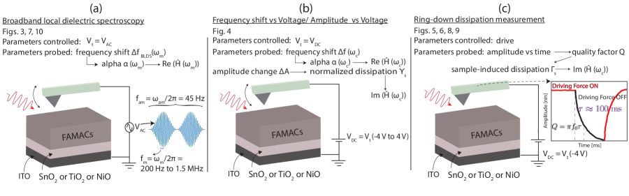
Let us begin by summarizing the equations we will use to connect scanning-probe data to sample properties. Interested readers are directed to Ref. 35 and Ref. 69 for a detailed derivation of the following equations. In our measurements we modulate the charge on the cantilever tip and the sample and observe the resulting change in the cantilever frequency or amplitude. This charge is modulated by physically oscillating the cantilever, by applying a time-dependent voltage to the cantilever tip, or by doing both simultaneously. A summary of the distinct measurements carried out below is given in Figure 1.
Changes in the cantilever frequency and amplitude may be expressed in terms of a transfer function which relates the voltage applied to the cantilever tip (the sample substrate is grounded) to the voltage dropped between the cantilever tip and the sample surface. The cantilever is modeled electrically as a capacitor while the sample is modeled as resistor operating in parallel with a capacitor (Figure 13). The resulting transfer function is given in the frequency domain by
| (1) |
which simplifies to
| (2) |
where defines the sample impedance . The transfer function can be viewed as a lag compensator whose time constant and gain parameter are given by, respectively,
| (3) |
We give the time constant the subscript “fast” because of the time constant’s similarity to “” measured in impedance spectroscopy 35. We show experimentally below that ; consequently, . This simplification allows us to associate photo-induced changes in cantilever frequency and amplitude to photo-induced changes in sample resistance or, equivalently, sample conductivity.
The complex-valued transfer function in Eq. 2 has a real part which determines the in-phase forces and an imaginary part which determines the out-of-phase forces acting on the cantilever. We show the equivalent circuit and plot the shape of transfer function in Figure 13. The frequency shift measurements presented in Figure 4b probe the real part of the transfer function,
| (4) |
where is the resonance frequency, is the spring constant, and is the amplitude, respectively, of the cantilever; is the in-phase force; is the cantilever capacitance computed at rest with the cantilever at its equilibrium position; , with primes indicating derivatives with respect the tip-sample distance; ; is the voltage applied to the cantilever tip; and is the surface potential. The variable plotted in Figure 4a is a voltage-normalized frequency shift, the curvature of the \latinvs. data defined by the equation and given by
| (5) |
From Eq. 5 we can see that is sensitive to the real part of the transfer function at frequency , with additional contributions from in-phase forces present at low frequency (. The sample-induced dissipation plotted in Figures 4a, 5, 6, 8, and 9 is sensitive to the out-of-phase part of the transfer function,
| (6) |
where is the out-of-phase force acting on the cantilever. The voltage-normalized dissipation plotted in Figure 4b is related to through the equation . The BLDS measurements of Figures 3, 7, and 10 are frequency-shift measurements that probe the response of the sample to an oscillating applied voltage,
| (7) |
where and are the frequency and amplitude, respectively, of the oscillating applied voltage and we have assumed the amplitude modulation frequency is much smaller than (see Experimental Section in Supporting Information). The imaginary part of the transfer function is significant only at the frequency where the real part of the transfer function starts to roll-off. The term in Eq. 7 containing the factors and is small as indicated by the BLDS spectra obtained at low light intensity over \ceSnO2 and \ceTiO2, Figure 3, where the majority of the response rolls off at . We conclude that the BLDS measurement primarily measures the in-phase forces at the modulation frequency. The voltage-normalized frequency shift plotted in Figures 3, 7, 10 is related to by
| (8) |
Figure 1 summarizes the experimental set-up and the measured quantity in each of the three different scanning probe measurements employed in this manuscript.
3.2 Experimental findings
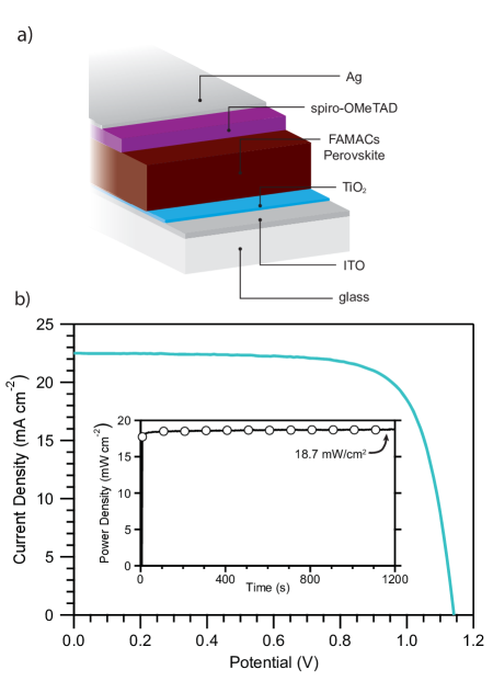
We now present data acquired on the FAMACs samples prepared on a range of substrates. All of the substrates (\ceTiO2, \ceSnO2, \ceNiO, \ceITO) are planar structures. The FAMACs thickness was ; the thickness of ETL/HTL layer was with average roughness of , and the thickness of the ITO was with an average roughness of . The samples were illuminated from the top. The high absorption coefficient of the perovskite film means that electron and hole generation was confined to the top of the sample, a distance significantly smaller than the thickness of the FAMACs layer. Figure 2 shows device-performance data for a representative FAMACs film prepared on a \ceTiO2 substrate; this data demonstrates the high quality of the films used in this study.
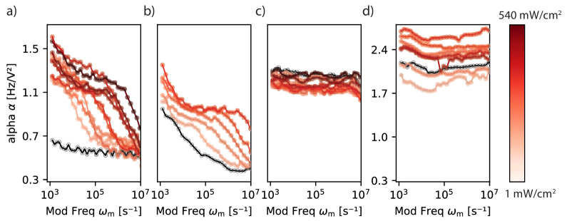
Figure 3 shows Broadband Local Dielectric Spectroscopy data (BLDS 50, Fig. 1a) acquired of films prepared on \ceTiO2, \ceSnO2, \ceITO, and \ceNiO substrates (see the Experimental Section in Supporting Information). In Figure 3, a decrease in at large voltage-modulation frequency indicates qualitatively that not all of the sample charge is able to follow the modulated tip charge. In our impedance model of the tip-sample interaction, Figure 13, this decrease is attributed to the roll-off of the tip-sample circuit. A light-dependent change in the roll-off frequency is consistent with sample conductivity increasing with increasing light intensity or, in other words, a decrease in the time constant with light. In Figure 3 we clearly see a roll-off of the \latinvs. curves that depends on the light intensity in the case of electron-acceptor substrates (\ceTiO2 and \ceSnO2), whereas in the case of the \ceNiO-(hole acceptor) and \ceITO-substrate samples, is independent of both and light intensity.
For the rest of this section of the manuscript, we compare the light and frequency dependence of the conductivity in the \ceTiO2 and \ceSnO2-substrate samples. Both samples show a light-dependent roll-off of the dielectric response. However some significant differences can also be seen:
-
1.
In the dark, the \ceSnO2-substrate sample is more conductive than the \ceTiO2-substrate sample as seen by their dark BLDS response curves.
-
2.
The conductivity of the \ceSnO2-substrate sample is more strongly affected by light than that of the \ceTiO2-substrate sample; the roll-off moves to higher frequencies for the same light intensity for the \ceSnO2-substrate sample compared to the \ceTiO2-substrate sample.
These light-dependent conductivity effects can be confirmed through quasi-steady-state measurements of the cantilever frequency shift () \latinvs. applied tip voltage () and cantilever amplitude () \latinvs. applied tip voltage (Figure 1b). In these measurements the cantilever is driven using constant-amplitude resonant excitation and the cantilever amplitude and frequency shift are recorded at each applied . By fitting the measured frequency shift and amplitude data to Eq. 27 and Eq. 32 respectively — see Figure 14 for representative curves and Sec. 8 for calculation details — we can calculate the curvature () change and a voltage-normalized sample-induced dissipation constant (). These values are not affected by the tip voltage sweep width; the large wait time () employed at each applied tip voltage ensure that the measured response is a steady-state response.
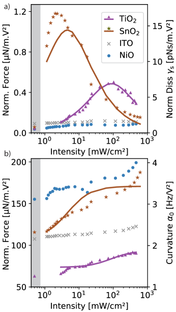
Figure 4a shows the sample-induced dissipation measured through the amplitude-voltage method. In this measurement we are sensitive to the out-of-phase response of the sample at the cantilever frequency. Figure 15 illustrates the predicted dependence of the curvature and sample-induced dissipation on light intensity. A non-linear increase in dissipation which reaches a maximum and then decreases with light intensity can be explained by the existence of a time constant that increased monotonically with light intensity. At high light intensities, the sample reaches its high-conductivity state. When is less than , most of the sample charge responds instantaneously to changes in the tip position, leading to a decrease in the out-of-phase force acting on the cantilever and a reduction in sample-induced dissipation. We see for both the \ceTiO2-substrate sample and the \ceSnO2-substrate sample that dissipation reached a maximum before decreasing when the light intensity was increased monotonically. Figure 4b shows that, concomitant with a dissipation peak, there is a non-linear change in the in-phase response at the cantilever frequency, observed as a changes in the curvature of the frequency shift \latinvs. applied tip voltage parabola ().
The data of Figure 4, which primarily measures sample response at a single frequency (), corroborates the data of Figure 3 which shows the sample response at multiple frequencies. The solid lines in Figure 4 are a fit to a one-time-constant impedance model described in Ref. 35 and summarized in Sec. 3.1. The model qualitatively explains the seemingly-anomalous peak in sample-induced dissipation \latinvs. light intensity data over both \ceTiO2 and \ceSnO2. The one-time-constant model only qualitatively describes the charge dynamics in the \ceSnO2-substrate sample; adding further electrical components to the sample-impedance model, justified by the double roll-off seen in the Figure 3b data, would improve the \ceSnO2-substrate fits in Figure 4.
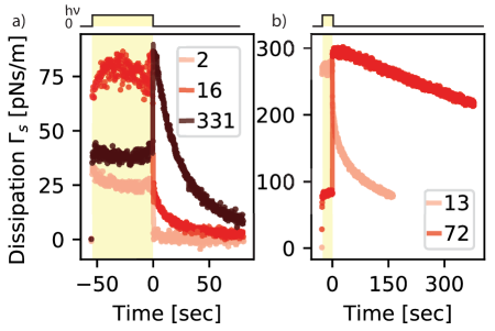
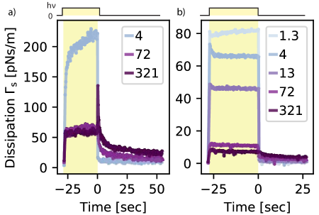
We observed the dynamics of in real time through two different methods. In Figure 5a, we show how the dissipation changes for the \ceTiO2-substrate sample for different light intensities. Here we inferred sample-induced dissipation by measuring changes in the quality factor of the cantilever through a ring-down measurement (Figure 1c and Sec. 9). The recovery of dissipation clearly had two distinct timescales — a fast component and a slow component. In Figures 5a and b, when the light was switched on, there was a large and prompt ( ) increase in dissipation followed by a small and much slower increase that lasted for or longer. The presence of the slow component was especially clear when the light intensity was greater than the light intensity giving the maximum dissipation. Whether the dissipation increased or decreased when the light was switched off depended on the value that (\latini.e. sample conductivity) reached during the light-on period. At low light intensities ( and for the \ceTiO2-substrate sample, Figure 5a, and for the \ceSnO2-substrate sample, Figure 5b), the dissipation decreased when the light was switched off, indicating that was . On the other hand, the initial rise in when the light was switched off for the dataset in Figure 5a and the dataset in Figure 5b is consistent with a light-on being . In such a case, when the light was switched off, the promptly increased in as approached the value of . Subsequently, gradually decreased over ’s of seconds as became .
In Figure 5b, we show a time-resolved light-induced dissipation measurement for the \ceSnO2-substrate sample. The slow part of the recovery of dissipation was extremely slow ( ) at room temperature. This slow recovery indicates that the \ceSnO2-substrate sample retained its conductive state for a much a longer time than did the \ceTiO2-substrate sample. Interestingly, the slow time constant for dissipation recovery showed a dependence on the pre-soak intensity. As the light intensity increased, the dissipation recovery time constant became slower. The underlying process responsible for the dissipation recovery is thus light-intensity dependent. The prompt recovery in conductivity was too fast to resolve, limited by the time resolution of the ringdown measurement.
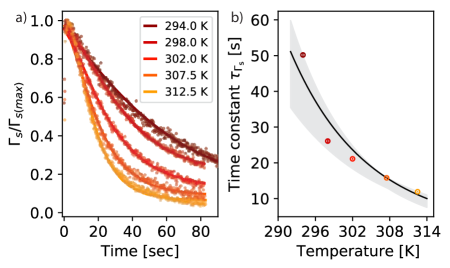
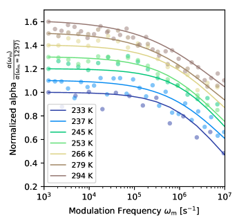
In Figure 6a we show the temperature dependence of the slow part of the dissipation recovery. In Figure 6b we plot the calculated dissipation-recovery time constant () for the data in (a) versus temperature. The slow part of the dissipation recovery is activated with an activation energy for the \ceTiO2-substrate sample. For the \ceSnO2-substrate sample, the slow part of the dissipation recovery did not show an appreciable change in the accessible to temperature window (Figure 20). The dissipation recovery of the \ceSnO2-substrate sample was much slower than \ceTiO2-substrate sample at room temperature, implying .
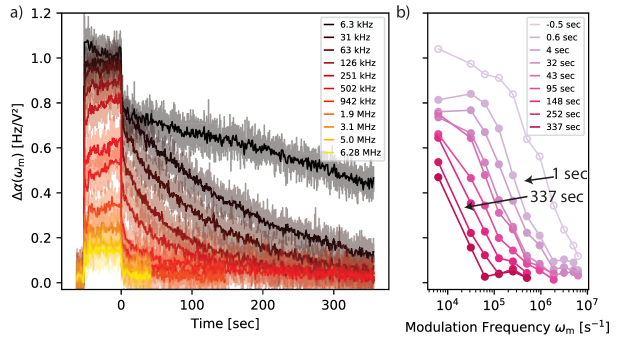
To further show the presence of two distinct recovery timescales, we examined the fixed-frequency dielectric response for the \ceTiO2-substrate sample (Figure 7). Here we illuminate the sample and measure the time-resolved dielectric response at a fixed modulation frequency (). The response at each corresponds to the in-phase force at that modulation frequency. By doing the measurement at different modulation frequencies, we can visualize the time evolution of the full dielectric response curve in the dark after the light was turned off. Comparing the reconstructed dielectric response curves for time just before switching off the light (open circles) and after switching off the light (closed circles) shows a fast ( ) decrease in the roll-off frequency (\latini.e. a decrease in sample conductivity). This fast decrease was followed by a slow decrease lasting ’s of seconds before the dark state is reached. Thus sample conductivity was thus decreasing on multiple distinct timescales in the dark. While the dielectric response curve measurement produces a more comprehensive picture of the conductivity recovery compared to the single-shot ring-down measurements, it is an inherently slower measurement than the ring-down measurement and is potentially affected by hysteresis since it requires a long resting time ( between each measurement).
We attribute changes in dissipation and the BLDS response to changes in sample resistance (or conductivity) rather than sample capacitance . In Figures 3a,b and Figure 7, the high frequency response, determined by the ratio , is independent of the light intensity. The similar high frequency response implies that does not depend strongly on the light intensity. Therefore we can make the approximation that changes in the BLDS response primarily reflect changes in the sample resistance, or equivalently, sample conductivity. In a mixed ionic-electronic conductor, one might expect to report on changes in the ambipolar resistance (or conductivity) and the measured dynamics of the resistance changes would be determined by the slowest diffusing species 74. Using a more accurate transmission-line model of sample impedance, we show below in Sec. 4.3 that our electric force microscope measurements are probing the total sample conductivity (Eqs. 23).
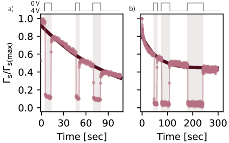
To verify that the tip electric field is not the cause of the slow dissipation recovery, we switched off the tip voltage during acquisition of the dissipation recovery transients for different durations of time (Figure 8). We find negligible differences in the dissipation recovery transient when the tip voltage is switched off. We conclude that we are passively observing fluctuations in the sample whose dynamics are unaffected by the tip charge, \latini.e. we are operating in the linear-response regime of fluctuation-dissipation theorem. This finding indicates that represents sample conductivity that continues to relax irrespective of the tip electric field at the surface. This experimental result also rules out that changes in the conductivity are due to tip-induced charging and discharging of the interfacial redistribution of electronic and ionic charges at the perovskite-substrate interface.
Lead halide perovskites are worse thermal conductors compared to many organic semiconductors and at normal solar cell operating conditions, thermal-gradient-induced ion migration away from the light source due to the Soret effect is a possibility.75. However, we can rule out temperature variations induced due to light as the main cause of the slow dissipation recovery. The slow recovery is evident at even very modest light intensity of in Figure 5a and in Figure 5b. Following the analysis of photo thermal effects presented in Ref. 67, even would cause change in temperature. Additional analysis of the data presented in Figure 3 is provided in Figure 21 and Figure 22 and shows that essentially decreases logarithmically with light intensity (). Photothermal effects would be inconsistent with this experimental result.
We next measure the effect of significantly reduced ion motion on the dynamics of sample conductivity. Several reports suggest that, in a similar temperature range (), the effect of ion motion on measurements can be significantly reduced or eliminated by cooling the sample. This reduction manifests itself in device measurements as a reduced hysterisis in curves.76, 77 This motion-reduction hypothesis was investigated here by measuring dissipation recovery dynamics at low temperature (). In Figure 9 we see that the dissipation \latinvs. light intensity showed a similar behavior to the room temperature measurements of Figure 5 for the duration of illumination. This finding is further corroborated by BLDS measurements at a fixed light intensity taken at different temperatures for the \ceSnO2-substrate sample. This data shows that the value of in \ceSnO2 is unaffected by temperature (Figure 10) and is decreased with increasing light intensity even as the temperature is lowered. Interestingly, there is essentially no slow recovery of dissipation when compared with room temperature (Figure 9). The absence of slow recovery dynamics is consistent with the hypothesis that the slow recovery (Figure 9) is determined by ion motion, which is substantially arrested at . The total conductivity of the sample under illumination is dominated by the electronic carriers.19 The interaction of these electronic carriers with the slow moving ions determines the dynamics of the light-induced conductivity decrease when the light is switched off.
4 Discussion
4.1 Summary of experimental conductivity findings
We have observed photo-induced changes in conductivity perturbing the electrostatic forces oscillating both in-phase and out-of-phase with the cantilever motion. Light-induced changes in the in-phase force leads to the frequency-shift effects seen in Figures 3, 4b, and 7, while light-induced changes in the out-of-phase force causes the dissipation phenomena apparent in Figures 4b, 5, 6, and 8. Above we concluded from the high-frequency data in Figures 3a,b and Figure 7 that the light-dependence of both the dissipation and the BLDS response could be attributed to changes in sample resistance (or conductivity ) rather than sample capacitance . Measuring dissipation thus allowed us to track changes in sample conductivity in real time as a function of light intensity and temperature. The resulting picture of sample conductivity dynamics was corroborated by monitoring the sample’s dielectric spectrum in real time at selected frequencies.
We found that the observed sample conductivity in FAMACs
-
1.
was substrate dependent, and
-
(a)
was comparatively low in the dark and dependent on light intensity over \ceTiO2 and \ceSnO2 but
-
(b)
was comparatively high in the dark and independent of light intensity over \ceITO and \ceNiO.
-
(a)
The light-dependent conductivity of FAMACs grown over \ceTiO2 and \ceSnO2 was studied in detail. We found that the conductivity in these samples
-
2.
increased rapidly ( ) when light was applied;
-
3.
had a steady-state value which increased with light intensity, with this increase being temperature-independent over \ceSnO2;
-
4.
retained its light-on value when the light was turned off at room temperature
-
(a)
for 10’s of seconds over \ceTiO2 and
-
(b)
for 100’s of seconds over \ceSnO2;
-
(a)
-
5.
relaxed from a light-on value to a light-off value above room temperature with a rate that
-
(a)
increased with increasing temperature over \ceTiO2, with a large activation energy, , usually associated with vacancy or halide-ion motion but
-
(b)
had no measurable temperature dependence over \ceSnO2; and
-
(a)
-
6.
relaxed from its light-on to its light-off value essentially instantaneously at low temperature.
We wish to explain these findings microscopically. The first step in doing so is to consider the source of the observed conductivity.
4.2 Conductivity sources
There are two obvious contributions to sample conductivity to consider — electronic and ionic. Light-dependent electronic conductivity is expected in a semiconductor like a lead-halide perovskite in which light absorption in the bulk creates free electrons and holes. If the conductivity is dominated by electronic conductivity then one would expect the conductivity to increase rapidly under illumination and be intensity-dependent, consistent with Observation 1a. Further experiments show that the fast time constant is essentially linear in light intensity (Figures 21 and 22). When the light is turned off, however, the electronic conductivity should decay to its light-off value on the timescale of the carrier lifetime — nanoseconds to microseconds in lead-halide perovskites 78, 79, 80, 81, 82, 7. Instead we find that the light-induced conductivity over \ceTiO2 and \ceSnO2 persisted for 10’s to 100’s of seconds when the light was turned off.
The observed sample conductivity could alternatively be dominated by ionic conductivity. Perovskites are expected to have a high concentration of charged vacancies 1, 2, 3; the vacancy concentration depends on the electron Fermi level and on the chemical potential (\latini.e. the concentration) of the chemical species present during film growth 1, 3. Prior studies have demonstrated that the electron Fermi level of the perovskite can moreover be altered by changing the work function of the substrate 11, 83, 84, 13, with recent work demonstrating that the substrate can change the stoichiometry of the perovskite film as well 85. Based on the observations of Refs. 11, 13, 83, and 84, and we would expect a high halide-vacancy concentration in a perovskite grown over a hole-injecting substrate like \ceNiO or \ceITO, in agreement with the observed trends in the light-off conductivity, Observation 1b. If the sample conductivity is dominated by ionic conductivity, however, we would not expect the ionic conductivity to be linearly proportional to light intensity and independent of temperature (Observations 3), nor would we expect ionic conductivity to retain a memory of the light intensity for 10’s to 100’s of seconds in the dark (Observations 3 and 4).
In summary, the observed conductivity has attributes of both electronic and ionic conductivity. Tirmzi and coworkers observed a similarly puzzling long-lived photo-induced conductivity in their related prior dissipation-microscopy experiments on \ceCsPbBr3. They posited that photo-induced electrons and holes were being captured by charged vacancies existing in the film 35:
| (9a) | ||||
| (9b) | ||||
The idea of a weakly-trapped electron and hole, and respectively, was proposed as a way to simultaneously account for the conductivity’s light dependence, memory, and large activation energy. The Eq. 9 proposal required the and species to dominate the conductivity, which the Ref. 35 authors noted was seemingly at odds with the idea of a weakly-trapped electron and hole. The notion that and (or and ) diffuse together as a unit is the central idea underlying the concept of ambipolar conductivity, although the authors of Ref. 35 did not employ this term. We will consider ambipolar conductivity in more detail shortly.
The hypothesis that we are observing ambipolar conductivity resolves some but not all of our puzzling conductivity observations. We need another key new idea. Since the work of Tirmzi \latinet al., Kim, Maier, and coworkers 19 have used multiple physical measurements to demonstrate that light induces a large enhancement in the ionic conductivity of methylammonium lead iodide. To explain this observation they proposed a reaction of photo-induced holes with neutral iodine atoms in the lattice that generates neutral interstitial iodines and charged, mobile iodine vacancies:
| (10) |
In their view, the application of light increases the concentration of holes, , which shifts the Eq. 10 equilibrium to the right; this shift increases the concentration of which in turn raises the ionic conductivity. That the halide-vacancy concentration depends on is expected, given the dependence of defect concentration on electron Fermi level 1, 3, 9. The significance of the Kim \latinet al. data is that it experimentally demonstrates the existence of light-induced changes in ionic conductivity and quantifies the size of the effect. For our purposes, the Eq. 10 observation provides a better starting point for understanding our observations than does the Eq. 9 conjecture. To describe our further observations it is helpful to augment Eq. 10 to include both the holes and electrons created by light absorption:
| (11) |
Equation 11 indicates the presence, after illumination, of cationic vacancies and charge-compensating electrons, both of which are mobile. We should therefore formulate the sample’s dielectric response in terms of its ambipolar conductivity 86.
4.3 Ambipolar conductivity
The relevance of ambipolar conductivity to understanding light-dependent phenomena in mixed ionic-electronic conductors like metal halide perovskites is just becoming apparent 74. In our prior scanned-probe study of \ceCsPbBr3 we modeled the sample as a resistor and capacitor connected in parallel. The quantitative response of an ambipolar sample in an electric force microscope experiment has not, to our knowledge, been considered before 87. In order to ascertain the dependence of measured dissipation and frequency shift on the sample’s electronic and ionic conductivity, in this section we apply a more physically accurate transmission-line model of the sample’s dielectric response 88.
The starting point for modeling the response of a charged cantilever to a conductive sample is the transfer function in Eq. 1, which may be simplified to read
| (12) |
with the sample impedance. The impedance of a mixed ionic-electronic conductor was first derived in detail for various electrode models by McDonald 89 but the derivation ignored space-charge regions near the contacts. A more tractable and generalizable transmission-line treatment of a mixed ionic-electronic conductor was introduced by Jamnik and Maier 88. Their approach has since been applied to calculate the impedance spectra of materials ranging from ion-conducting ceramics 90, 91 to lead-halide perovskite photovoltaics 92, 93. Let us use the impedance formula given in Ref. 88 (correctly written as Eq. 61 in Ref. 90) to calculate an approximate for our sample.
In the Ref. 88 model, the sample is assumed to contain two mobile charged carriers, where the first species is ionic (charge , concentration , conductivity ) and the second species is electronic (charge , concentration , conductivity ). The associated ionic and electronic resistance is given by and , respectively, with the sample thickness and the sample cross-sectional area. Two other variables arise naturally in the transmission-line treatment. The first is the chemical capacitance 88,
| (13) |
with the electronic unit of charge, Boltzmann’s constant, and temperature. It is reasonable to assume that 94, 95, 79, 2; in this limit, , and the chemical capacitance is determined by the concentration of the electronic carriers alone. The second central variable is the ambipolar diffusion constant, defined as
| (14) |
which simplifies to
| (15) |
In Ref. 88 the electrodes are assumed to be symmetric and described by a distinct interface impedance for ionic and electrical carriers:
| (16a) | ||||
| (16b) | ||||
with the subscript indicating the carrier and the superscript indicating that the resistance and capacitance is associated with the sample/electrode interface. We can rearrange Jamnik and Maier’s central impedance result to read
| (17) |
with the low- and high-frequency limiting impedance given by
| (18a) | ||||
| (18b) | ||||
and the time constant defined as
| (19) |
Our sample has a bottom contact consisting of a grounded electrical conductor and a top contact consisting of an electrically biased tip-sample capacitor. The impedance of the tip-sample capacitor operating in series with the electrically ground sample is already captured in Eq. 12. To capture the impedance of our sample in the transmission-line formalism we assume that the electrodes (1) are ohmic for the electronic carriers, , and (2) are blocking for the ions, and consequently . Under these simplifying assumptions, . In reality the sample’s bottom face is metal-terminated while its top face is vacuum terminated; although the sample is not strictly symmetric, under our electrode assumptions the transmission-line impedance model should nevertheless give accurate guidance on what sample properties our scanned probe measurements are probing. Substituting for the expressions for and in the ion-blocking limit in Eq. 17 and simplifying the result we obtain
| (20) |
with
| (21) |
and
| (22) |
As long as or , the sample impedance will be operating in the high frequency limit where . The transfer function describing the tip-sample interaction in this high-frequency limit can be approximated as (Figure 11a)
| (23a) | ||||
| with | ||||
| (23b) | ||||
Somewhat surprisingly, the rolloff of depends not on the ambipolar conductivity but on the total conductivity, .
| case I (dark) | case II (dark) | case III (light) | ||||||
| quantity | unit | value | Ref | value | Ref | value | Ref | |
| A. | 94 | 95 | 79 | |||||
| 2 | 2 | |||||||
| 19 | 19 | 19 | ||||||
| 19 | 19 | 19 | ||||||
| B. | ||||||||
| C. | ||||||||
We can check the validity of the approximate Eq. 23 transfer function by comparing with calculated using the full impedance expression of Eq. 20. To calculate the transfer function requires knowledge of , , , , , and . To our knowledge, no single study provides values for all these quantities for FAMACs. We therefore turn to the MAPI literature for order-of-magnitude estimates of these quantities; see Table 1A. The dark estimates vary from (case I (dark)) to (case II (dark)). For under illumination (case III) we expect the value to be similar or higher than the corresponding dark value. We calculated and from the Ref. 19 conductivities taking , the film thickness, and , our estimate of the cantilever-tip area. In Table 1A we have linearly scaled the conductivities observed in Ref. 19 to account for the higher light intensities used in our measurements. The value of (Table 1B) was calculated using Eq. 13 and the values for and given in Table 1A. We take where 96 is the static dielectric constant and 97 is the Debye length. We use , a reasonable upper-bound number taking in account the experimental tip-sample separation 98, 69. Using Table 1A-B values and the above estimates for and we obtain the frequencies , , and given in Table 1C.
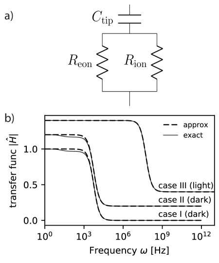
We plot the resulting approximate and exact transfer function for two dark conditions and one light condition in Figure 11b. This exercise confirms that is indeed a valid approximation. The effect of on the transfer function is only significant when or are within an order of magnitude of . A slight breakdown of the Eq. 23 approximation can be seen in the Figure 11b transfer-function plots for case I (dark) and II (dark) at low frequency. In most scenarios this breakdown is unlikely to occur because and in this limit .
4.4 Explaining the conductivity findings
Now that we have established that the measurements in this manuscript probe total conductivity, we will look at how the concentrations of and and the Eq. 11 scheme can be used to rationalize differences in the conductivity and conductivity relaxation between different substrates.
We would expect the concentration of holes in the dark (and therefore ) to be high over the \ceITO and \ceNiO and low over \ceTiO2 and \ceSnO2 11, 83, 84, 13. Observations 1a, 1b, and 3 follow from Eq. 10 and the assumption that over \ceITO and \ceNiO while over \ceTiO2 and \ceSnO2. A change in the sample conductivity due to the substrate is indirectly implied in the results of Refs. 11, 13, 83, and 84 where the work function of the perovskite surface was shown to change as a function of substrate work function. Our data likewise shows a substrate effect, only here we probe the conductivity directly. The high absorption coefficient of the perovskite means that electrons and holes are primarily generated in the top of our -thick films. Possible processes that may exist and can directly or indirectly change the material and therefore the total conductivity include substrate induced strain effects,99, 100 substrate dependent sample microstructure and stoichiometery,85 and heterogeneous doping.101 Our current results are largely inconsistent with heterogeneous doping effects. Substrate effects through heterogeneous doping are going to be limited to a thin layer near the perovskite-substrate interface and are more prominent when the substrates is mesoporous. In this layer, the concentration of both electronic and ionic charges is determined by the substrate perovskite interaction.101 This is inconsistent with the Figure 8 results and the thickness of the films () used in our measurements.
Under illumination the concentration of is high; the forward reaction in Eq. 11 proceeds rapidly, creating charged vacancies and free electrons resulting in the promptly appearing light-dependent conductivity of Observations 2 and 3. The relative similarity of the dependence of the conductivity on time, light, and temperature over \ceSnO2 and \ceTiO2 suggests to us that the light-on conductivity in \ceTiO2 is also likely dominated by electronic conductivity. According to Eq. 23b, for the observed total conductivity to return to its light-off value, both and need to return to their dark values. Observation 4 is explained by the back reaction in Eq. 11 having a high activation energy and proceeding slowly. The differences in the timescale of the conductivity relaxation over \ceTiO2 and \ceSnO2, Observations 5a and 5b, requires a difference in this activation energy or in the mobility of ions in the FAMACs grown on the two substrates. Christians and coworkers have reported a differences in the distribution of ions in aged devices incorporating \ceTiO2/FAMACs and \ceSnO2/FAMACs interfaces, as quantified by time-of-flight secondary ion mass spectrometry 30; these differences are consistent with the slower relaxation seen here over \ceSnO2.
The fast conductivity relaxation seen at low temperature, Observation 6, seems \latinprima facia at odds with the slow and activated recovery seen at room temperature, Observations 4 and 5. We should consider, however, that once generated, the iodine vacancy, , and the neutral iodine interstitial defect, , are expected to diffuse away from each other (to maximize entropy). In mixed-halide perovskites light has been shown to promote halide segregation and in these systems the rate of segregation depends on the light intensity 102, 103. One might therefore expect the Eq. 11 back reaction underlying Observations 4 and 5 to be diffusion limited; in this limit the activation energy of the back reaction is the governing and diffusion. The we observe over \ceTiO2 is consistent with the activation energy measured for halide-vacancy motion in lead-halide perovskites 104, 102, 15. The activation energy observed is the activation energy for the total conductivity relaxation. This will in turn depend on the concentration electronic and ionic species, but also on their mobility. We note that the light intensity primarily determines the concentration of both ionic and electronic carriers and was kept constant for variable temperature measurements. While we are not directly probing the activation energy of ionic diffusion (and therefore the ionic mobility), it is the most likely term to change in the small temperature window used in the measurement. At low temperature we expect the vacancy diffusion to be suppressed and consequently might expect the back reaction to be now fast because the and species generated by the forward Eq. 11 reaction remain in close proximity. This prediction is indeed consistent with Observation 6.
Subsequent reactions are also possible. Based on Minns \latinet al.’s 105 X-ray and neutron diffraction studies of \ce(CH3NH3)PbI3, for example, we expect the iodine interstitials to form stable interstitial \ceI2 moieties. The concentration of these \ceI2 moieties (and the coupled vacancy concentration) can be decreased by lowering the temperature. Additionally, theory predicts the iodine interstitial to be a hole trap, 106. Such reactions and the decreased concentration of \ceI2 moieties, if present, might likewise explain the significant differences in recovery seen over \ceTiO2 and \ceSnO2, Observations 5a and 5b.
5 Conclusions
Here we have used measurements of sample-induced dissipation and sample dielectric spectra, backed by a rigorous theory of the cantilever-sample interaction 67, 35, 69, to carry out time-resolved studies of photo-induced changes in the total conductivity of a mixed-species lead-halide perovskite semiconductor thin film prepared on a range of substrates. Comparison of low temperature and room temperature data and a transmission-line model analysis of mixed ionic-electronic conductivity reveals that the observed photo-induced changes in cantilever frequency and dissipation report on changes in total sample conductivity, . This insight establishes scanning-probe broadband local dielelectric spectroscopy measurements as a method for quantifying local photo-conductivity in semiconductors and other photovoltaic materials.
In the FAMACs samples studied here, light-induced changes in total conductivity relaxed on a time scale of ’s to ’s of seconds, with an activation energy of over \ceTiO2; such a large activation energy is generally attributed to ion/vacancy motion 104, 102, 15. We rationalized these findings using the idea of light-induced vacancies recently proposed by Kim \latinet al.19 In addition to the seemingly puzzling light-induced conductivity behavior explored here, light-induced creation of vacancies may also explain other light-induced anomalous behavior seen in lead halide perovskites including memory effects 25.
SUPPORTING INFORMATION AVAILABLE The Supporting Information contains: Experimental details regarding scanning probe microscopy; experimental details for Fig. 4; spatial variation the BLDS response; representative AFM images; steady state and transient surface potential; fit detail for Fig. 6; effect of below band gap illumination on dissipation; for \ceSnO2-substrate sample.
AUTHOR INFORMATION
Corresponding Author
∗E-mail: jam99@cornell.edu
Faculty webpage:
http://chemistry.cornell.edu/john-marohn
Research group webpage:
http://marohn.chem.cornell.edu/
Notes
The authors declare no competing financial interest.
A.M.T, R.P.D, and J.A.M acknowledge the financial support of the U.S. National Science Foundation (Grant DMR-1709879). J.A.C. was supported by the Department of Energy (DOE) Office of Energy Efficiency and Renewable Energy (EERE) Postdoctoral Research Award under the EERE Solar Energy Technologies Office administered by the Oak Ridge Institute for Science and Education (ORISE) for the DOE under DOE contract number DE-SC00014664.
References
- Yin \latinet al. 2014 Yin, W.-J.; Shi, T.; Yan, Y. Unusual Defect Physics in CH3NH3PbI3 Perovskite Solar Cell Absorber. Appl. Phys. Lett. 2014, 104, 063903
- Walsh \latinet al. 2015 Walsh, A.; Scanlon, D. O.; Chen, S.; Gong, X. G.; Wei, S.-H. Self-Regulation Mechanism for Charged Point Defects in Hybrid Halide Perovskites. Angew. Chem. Int. Ed. 2015, 54, 1791 – 1794
- Shi \latinet al. 2015 Shi, T.; Yin, W.-J.; Hong, F.; Zhu, K.; Yan, Y. Unipolar Self-doping Behavior in Perovskite CH3NH3PbBr3. Appl. Phys. Lett. 2015, 106, 103902
- Brandt \latinet al. 2015 Brandt, R. E.; Stevanovic, V.; Ginley, D. S.; Buonassisi, T. Identifying Defect-tolerant Semiconductors With High Minority-carrier Lifetimes: Beyond Hybrid Lead Halide Perovskites. MRS Comm. 2015, 5, 265 – 275
- Emara \latinet al. 2016 Emara, J.; Schnier, T.; Pourdavoud, N.; Riedl, T.; Meerholz, K.; Olthof, S. Impact of Film Stoichiometry on the Ionization Energy and Electronic Structure of CH3NH3PbI3 Perovskites. Adv. Mater. 2016, 28, 553 – 559
- Kim \latinet al. 2014 Kim, J.; Lee, S.-H.; Lee, J. H.; Hong, K.-H. The Role of Intrinsic Defects in Methylammonium Lead Iodide Perovskite. J. Phys. Chem. Lett. 2014, 5, 1312 – 1317
- Stranks 2017 Stranks, S. D. Nonradiative Losses in Metal Halide Perovskites. ACS Energy Lett. 2017, 2, 1515 – 1525
- Tress \latinet al. 2018 Tress, W.; Yavari, M.; Domanski, K.; Yadav, P.; Niesen, B.; Correa Baena, J. P.; Hagfeldt, A.; Graetzel, M. Interpretation and Evolution of Open-Circuit Voltage, Recombination, Ideality Factor and Subgap Defect States During Reversible Light-Soaking and Irreversible Degradation of Perovskite Solar Cells. Energy Environ. Sci. 2018, 11, 151 – 165
- Senocrate \latinet al. 2018 Senocrate, A.; Yang, T.-Y.; Gregori, G.; Kim, G. Y.; Grätzel, M.; Maier, J. Charge Carrier Chemistry in Methylammonium Lead Iodide. Solid State Ionics 2018, 321, 69 – 74
- Moore \latinet al. 2015 Moore, D. T.; Sai, H.; Tan, K. W.; Smilgies, D.-M.; Zhang, W.; Snaith, H. J.; Wiesner, U.; Estroff, L. A. Crystallization Kinetics of Organic–Inorganic Trihalide Perovskites and the Role of the Lead Anion in Crystal Growth. J. Am. Chem. Soc. 2015, 137, 2350 – 2358
- Miller \latinet al. 2014 Miller, E. M.; Zhao, Y.; Mercado, C. C.; Saha, S. K.; Luther, J. M.; Zhu, K.; Stevanovic, V.; Perkins, C. L.; van de Lagemaat, J. Substrate-Controlled Band Positions in CH3NH3PbI3 Perovskite Films. Phys. Chem. Chem. Phys. 2014, 16, 22122 – 22130
- Schulz \latinet al. 2015 Schulz, P.; Whittaker-Brooks, L. L.; MacLeod, B. A.; Olson, D. C.; Loo, Y.-L.; Kahn, A. Electronic Level Alignment in Inverted Organometal Perovskite Solar Cells. Adv. Mater. Interfaces 2015, 2, 1400532
- Olthof and Meerholz 2017 Olthof, S.; Meerholz, K. Substrate-dependent Electronic Structure and Film Formation of MAPbI3 Perovskites. Sci. Rep 2017, 7, 3586
- Ono and Qi 2018 Ono, L. K.; Qi, Y. Research Progress on Organic–inorganic Halide Perovskite Materials and Solar Cells. J. Phys. D: Appl. Phys. 2018, 51, 093001
- Yang \latinet al. 2015 Yang, T.-Y.; Gregori, G.; Pellet, N.; Grätzel, M.; Maier, J. The Significance of Ion Conduction in a Hybrid Organic-Inorganic Lead-Iodide-Based Perovskite Photosensitizer. Angew. Chem. Int. Ed. 2015, 54, 7905 – 7910
- Delugas \latinet al. 2016 Delugas, P.; Caddeo, C.; Filippetti, A.; Mattoni, A. Thermally Activated Point Defect Diffusion in Methylammonium Lead Trihalide: Anisotropic and Ultrahigh Mobility of Iodine. J. Phys. Chem. Lett. 2016, 7, 2356 – 2361
- Zhu \latinet al. 2017 Zhu, X.; Lee, J.; Lu, W. D. Iodine Vacancy Redistribution in Organic-Inorganic Halide Perovskite Films and Resistive Switching Effects. Adv. Mater. 2017, 29, 1700527
- Li \latinet al. 2016 Li, C.; Tscheuschner, S.; Paulus, F.; Hopkinson, P. E.; Kießling, J.; Köhler, A.; Vaynzof, Y.; Huettner, S. Iodine Migration and Its Effect on Hysteresis in Perovskite Solar Cells. Adv. Mater. 2016, 28, 2446 – 2454
- Kim \latinet al. 2018 Kim, G. Y.; Senocrate, A.; Yang, T.-Y.; Gregori, G.; Grätzel, M.; Maier, J. Large Tunable Photoeffect on Ion Conduction in Halide Perovskites and Implications for Photodecomposition. Nat. Mater. 2018, 17, 445 – 449
- Senocrate \latinet al. 2017 Senocrate, A.; Moudrakovski, I.; Kim, G. Y.; Yang, T.-Y.; Gregori, G.; Grätzel, M.; Maier, J. The Nature of Ion Conduction in Methylammonium Lead Iodide: A Multimethod Approach. Angew. Chem. Int. Ed. 2017, 56, 7755 – 7759
- Yuan \latinet al. 2015 Yuan, Y.; Chae, J.; Shao, Y.; Wang, Q.; Xiao, Z.; Centrone, A.; Huang, J. Photovoltaic Switching Mechanism in Lateral Structure Hybrid Perovskite Solar Cells. Adv. Energy Mater. 2015, 5, 1500615
- Futscher \latinet al. 2018 Futscher, M. H.; Lee, J. M.; Wang, T.; Fakharuddin, A.; Schmidt-Mende, L.; Ehrler, B. Quantification of Ion Migration in CH3NH3PbI3 Perovskite Solar Cells by Transient Capacitance Measurements. arXiv:1801.085192018, arXiv e-Print
- deQuilettes \latinet al. 2016 deQuilettes, D. W.; Zhang, W.; Burlakov, V. M.; Graham, D. J.; Leijtens, T.; Osherov, A.; Bulovic, V.; Snaith, H. J.; Ginger, D. S.; Stranks, S. D. Photo-Induced Halide Redistribution in Organic–Inorganic Perovskite Films. Nat Comms 2016, 7, 11683
- Zhao \latinet al. 2015 Zhao, C.; Chen, B.; Qiao, X.; Luan, L.; Lu, K.; Hu, B. Revealing Underlying Processes Involved in Light Soaking Effects and Hysteresis Phenomena in Perovskite Solar Cells. Adv. Energy Mater. 2015, 5, 1500279
- Belisle \latinet al. 2017 Belisle, R. A.; Nguyen, W. H.; Bowring, A. R.; Calado, P.; Li, X.; Irvine, S. J. C.; McGehee, M. D.; Barnes, P. R. F.; O’Regan, B. C. Interpretation of Inverted Photocurrent Transients in Organic Lead Halide Perovskite Solar Cells: Proof of the Field Screening by Mobile Ions and Determination of the Space Charge Layer Widths. Energy Environ. Sci. 2017, 10, 192 – 204
- Wang 2018 Wang, Q. Fast Voltage Decay in Perovskite Solar Cells Caused by Depolarization of Perovskite Layer. J. Phys. Chem. C 2018, 122, 4822 – 4827
- Pockett \latinet al. 2015 Pockett, A.; Eperon, G. E.; Peltola, T.; Snaith, H. J.; Walker, A.; Peter, L. M.; Cameron, P. J. Characterization of Planar Lead Halide Perovskite Solar Cells by Impedance Spectroscopy, Open-Circuit Photovoltage Decay, and Intensity-Modulated Photovoltage/Photocurrent Spectroscopy. J. Phys. Chem. C 2015, 119, 3456 – 3465
- Zarazua \latinet al. 2016 Zarazua, I.; Bisquert, J.; Garcia-Belmonte, G. Light-Induced Space-Charge Accumulation Zone as Photovoltaic Mechanism in Perovskite Solar Cells. J. Phys. Chem. Lett. 2016, 7, 525 – 528
- Zarazua \latinet al. 2016 Zarazua, I.; Han, G.; Boix, P. P.; Mhaisalkar, S.; Fabregat-Santiago, F.; Mora-Seró, I.; Bisquert, J.; Garcia-Belmonte, G. Surface Recombination and Collection Efficiency in Perovskite Solar Cells From Impedance Analysis. J. Phys. Chem. Lett. 2016, 7, 5105 – 5113
- Christians \latinet al. 2018 Christians, J. A.; Schulz, P.; Tinkham, J. S.; Schloemer, T. H.; Harvey, S. P.; Tremolet de Villers, B. J.; Sellinger, A.; Berry, J. J.; Luther, J. M. Tailored Interfaces of Unencapsulated Perovskite Solar Cells for Hour Operational Stability. Nat. Energy 2018, 3, 68 – 74
- Saliba \latinet al. 2016 Saliba, M.; Matsui, T.; Seo, J.-Y.; Domanski, K.; Correa-Baena, J.-P.; Nazeeruddin, M. K.; Zakeeruddin, S. M.; Tress, W.; Abate, A.; Hagfeldt, A. \latinet al. Cesium-containing Triple Cation Perovskite Solar Cells: Improved Stability, Reproducibility and High Efficiency. Energy Environ. Sci. 2016, 9, 1989 – 1997
- Draguta \latinet al. 2018 Draguta, S.; Christians, J. A.; Morozov, Y. V.; Mucunzi, A.; Manser, J. S.; Kamat, P. V.; Luther, J. M.; Kuno, M. A Quantitative and Spatially Resolved Analysis of the Performance-Bottleneck in High Efficiency, Planar Hybrid Perovskite Solar Cells. Energy Environ. Sci. 2018, 11, 960 – 969
- Domanski \latinet al. 2017 Domanski, K.; Roose, B.; Matsui, T.; Saliba, M.; Turren-Cruz, S.-H.; Correa-Baena, J.-P.; Carmona, C. R.; Richardson, G.; Foster, J. M.; De Angelis, F. \latinet al. Migration of Cations Induces Reversible Performance Losses Over Day/Night Cycling in Perovskite Solar Cells. Energy Environ. Sci. 2017, 10, 604 – 613
- Leijtens \latinet al. 2013 Leijtens, T.; Eperon, G. E.; Pathak, S.; Abate, A.; Lee, M. M.; Snaith, H. J. Overcoming Ultraviolet Light Instability of Sensitized TiO2 With Meso-superstructured Organometal Tri-halide Perovskite Solar Cells. Nat Comms 2013, 4, 583
- Tirmzi \latinet al. 2017 Tirmzi, A. M.; Dwyer, R. P.; Hanrath, T.; Marohn, J. A. Coupled Slow and Fast Charge Dynamics in Cesium Lead Bromide Perovskite. ACS Energy Lett. 2017, 2, 488 – 496
- Denk and Pohl 1991 Denk, W.; Pohl, D. W. Local Electrical Dissipation Imaged by Scanning Force Microscopy. Appl. Phys. Lett. 1991, 59, 2171 – 2173
- Stipe \latinet al. 2001 Stipe, B. C.; Mamin, H. J.; Stowe, T. D.; Kenny, T. W.; Rugar, D. Noncontact Friction and Force Fluctuations between Closely Spaced Bodies. Phys. Rev. Lett. 2001, 87, 096801
- Cockins \latinet al. 2010 Cockins, L.; Miyahara, Y.; Bennett, S. D.; Clerk, A. A.; Studenikin, S.; Poole, P.; Sachrajda, A.; Grutter, P. Energy Levels of Few-electron Quantum Dots Imaged and Characterized by Atomic Force Microscopy. Proc. Natl. Acad. Sci. U.S.A. 2010, 107, 9496 – 9501
- Lekkala \latinet al. 2012 Lekkala, S.; Hoepker, N.; Marohn, J. A.; Loring, R. F. Charge Carrier Dynamics and Interactions in Electric Force Microscopy. J. Chem. Phys. 2012, 137, 124701
- Lekkala \latinet al. 2013 Lekkala, S.; Marohn, J. A.; Loring, R. F. Electric Force Microscopy of Semiconductors: Cantilever Frequency Fluctuations and Noncontact Friction. J. Chem. Phys. 2013, 139, 184702
- Cox \latinet al. 2016 Cox, P. A.; Flagg, L. Q.; Giridharagopal, R.; Ginger, D. S. Cantilever Ringdown Dissipation Imaging for the Study of Loss Processes in Polymer/Fullerene Solar Cells. J. Phys. Chem. C 2016, 120, 12369 – 12376
- Cox \latinet al. 2013 Cox, P. A.; Waldow, D. A.; Dupper, T. J.; Jesse, S.; Ginger, D. S. Mapping Nanoscale Variations in Photochemical Damage of Polymer/Fullerene Solar Cells With Dissipation Imaging. ACS Nano 2013, 7, 10405 – 10413
- Crider and Israeloff 2006 Crider, P. S.; Israeloff, N. E. Imaging Nanoscale Spatio-temporal Thermal Fluctuations. Nano Lett. 2006, 6, 887 – 889
- Stowe \latinet al. 1999 Stowe, T. D.; Kenny, T. W.; Thomson, D. J.; Rugar, D. Silicon Dopant Imaging by Dissipation Force Microscopy. Appl. Phys. Lett. 1999, 75, 2785 – 2787
- Luria \latinet al. 2012 Luria, J. L.; Hoepker, N.; Bruce, R.; Jacobs, A. R.; Groves, C.; Marohn, J. A. Spectroscopic Imaging of Photopotentials and Photoinduced Potential Fluctuations in a Bulk Heterojunction Solar Cell Film. ACS Nano 2012, 6, 9392 – 9401
- Yazdanian \latinet al. 2008 Yazdanian, S. M.; Marohn, J. A.; Loring, R. F. Dielectric Fluctuations in Force Microscopy: Noncontact Friction and Frequency Jitter. J. Chem. Phys. 2008, 128, 224706
- Hoepker \latinet al. 2011 Hoepker, N.; Lekkala, S.; Loring, R. F.; Marohn, J. A. Dielectric Fluctuations Over Polymer Films Detected Using an Atomic Force Microscope. J. Phys. Chem. B 2011, 115, 14493 – 14500
- Kuehn \latinet al. 2006 Kuehn, S.; Loring, R. F.; Marohn, J. A. Dielectric Fluctuations and the Origins of Noncontact Friction. Phys. Rev. Lett. 2006, 96, 156103
- Kuehn \latinet al. 2006 Kuehn, S.; Marohn, J. A.; Loring, R. F. Noncontact Dielectric Friction. J. Phys. Chem. B 2006, 110, 14525 – 145258
- Labardi \latinet al. 2016 Labardi, M.; Lucchesi, M.; Prevosto, D.; Capaccioli, S. Broadband Local Dielectric Spectroscopy. Appl. Phys. Lett. 2016, 108, 182906
- Bergmann \latinet al. 2014 Bergmann, V. W.; Weber, S. A. L.; Javier Ramos, F.; Nazeeruddin, M. K.; Grätzel, M.; Li, D.; Domanski, A. L.; Lieberwirth, I.; Ahmad, S.; Berger, R. Real-space Observation of Unbalanced Charge Distribution Inside a Perovskite-sensitized Solar Cell. Nat. Comms. 2014, 5, 5001
- Li \latinet al. 2015 Li, J.-J.; Ma, J.-Y.; Ge, Q.-Q.; Hu, J.-S.; Wang, D.; Wan, L.-J. Microscopic Investigation of Grain Boundaries in Organolead Halide Perovskite Solar Cells. ACS Appl. Mater. Interfaces 2015, 7, 28518 – 28523
- Yun \latinet al. 2016 Yun, J. S.; Seidel, J.; Kim, J.; Soufiani, A. M.; Huang, S.; Lau, J.; Jeon, N. J.; Seok, S. I.; Green, M. A.; Ho-Baillie, A. Critical Role of Grain Boundaries for Ion Migration in Formamidinium and Methylammonium Lead Halide Perovskite Solar Cells. Adv. Energy Mater. 2016, 6, 1600330
- Yuan \latinet al. 2017 Yuan, Y.; Li, T.; Wang, Q.; Xing, J.; Gruverman, A.; Huang, J. Anomalous Photovoltaic Effect in Organic-inorganic Hybrid Perovskite Solar Cells. Sci. Adv. 2017, 3, e1602164
- Garrett \latinet al. 2017 Garrett, J. L.; Tennyson, E. M.; Hu, M.; Huang, J.; Munday, J. N.; Leite, M. S. Real-Time Nanoscale Open-Circuit Voltage Dynamics of Perovskite Solar Cells. Nano Lett. 2017, 17, 2554-2560
- Collins \latinet al. 2017 Collins, L.; Ahmadi, M.; Wu, T.; Hu, B.; Kalinin, S. V.; Jesse, S. Breaking the Time Barrier in Kelvin Probe Force Microscopy: Fast Free Force Reconstruction Using the G-Mode Platform. ACS Nano 2017, 11, 8717 – 8729
- Salado \latinet al. 2017 Salado, M.; Kokal, R. K.; Calio, L.; Kazim, S.; Deepa, M.; Ahmad, S. Identifying the Charge Generation Dynamics in Cs+-based Triple Cation Mixed Perovskite Solar Cells. Phys. Chem. Chem. Phys. 2017, 19, 22905 – 22914
- Xiao \latinet al. 2017 Xiao, C.; Wang, C.; Ke, W.; Gorman, B. P.; Ye, J.; Jiang, C.-S.; Yan, Y.; Al-Jassim, M. M. Junction Quality of SnO2-Based Perovskite Solar Cells Investigated by Nanometer-Scale Electrical Potential Profiling. ACS Appl. Mater. Interfaces 2017, 9, 38373 – 38380
- Will \latinet al. 2018 Will, J.; Hou, Y.; Scheiner, S.; Pinkert, U.; Hermes, I. M.; Weber, S. A.; Hirsch, A.; Halik, M.; Brabec, C.; Unruh, T. Evidence of Tailoring the Interfacial Chemical Composition in Normal Structure Hybrid Organohalide Perovskites by a Self-Assembled Monolayer. ACS Appl. Mater. Interfaces 2018, 10, 5511 – 5518
- Birkhold \latinet al. 2018 Birkhold, S. T.; Precht, J. T.; Liu, H.; Giridharagopal, R.; Eperon, G. E.; Schmidt-Mende, L.; Li, X.; Ginger, D. S. Interplay of Mobile Ions and Injected Carriers Creates Recombination Centers in Metal Halide Perovskites Under Bias. ACS Energy Lett. 2018, 3, 1279 – 1286
- Birkhold \latinet al. 2018 Birkhold, S. T.; Precht, J. T.; Giridharagopal, R.; Eperon, G. E.; Schmidt-Mende, L.; Ginger, D. S. Direct Observation and Quantitative Analysis of Mobile Frenkel Defects in Metal Halide Perovskites Using Scanning Kelvin Probe Microscopy. J. Phys. Chem. C 2018, 122, 12633 – 12639
- Collins \latinet al. 2018 Collins, L.; Ahmadi, M.; Qin, J.; Liu, Y.; Ovchinnikova, O. S.; Hu, B.; Jesse, S.; Kalinin, S. V. Time Resolved Surface Photovoltage Measurements Using a Big Data Capture Approach to KPFM. Nanotechnology 2018, 29, 445703
- Coffey and Ginger 2006 Coffey, D. C.; Ginger, D. S. Time-Resolved Electrostatic Force Microscopy of Polymer Solar Cells. Nat. Mater. 2006, 5, 735 – 740
- Reid \latinet al. 2010 Reid, O. G.; Rayermann, G. E.; Coffey, D. C.; Ginger, D. S. Imaging Local Trap Formation in Conjugated Polymer Solar Cells: A Comparison of Time-Resolved Electrostatic Force Microscopy and Scanning Kelvin Probe Imaging. J. Phys. Chem. C 2010, 114, 20672 – 20677
- Giridharagopal \latinet al. 2012 Giridharagopal, R.; Rayermann, G. E.; Shao, G.; Moore, D. T.; Reid, O. G.; Tillack, A. F.; Masiello, D. J.; Ginger, D. S. Submicrosecond Time Resolution Atomic Force Microscopy for Probing Nanoscale Dynamics. Nano Lett. 2012, 12, 893 – 898
- Karatay \latinet al. 2016 Karatay, D. U.; Harrison, J. S.; Glaz, M. S.; Giridharagopal, R.; Ginger, D. S. Fast Time-resolved Electrostatic Force Microscopy: Achieving Sub-cycle Time Resolution. Rev. Sci. Instrum. 2016, 87, 053702
- Dwyer \latinet al. 2017 Dwyer, R. P.; Nathan, S. R.; Marohn, J. A. Microsecond Photocapacitance Transients Observed Using a Charged Microcantilever as a Gated Mechanical Integrator. Sci. Adv. 2017, 3, e1602951
- Crider \latinet al. 2007 Crider, P. S.; Majewski, M. R.; Zhang, J.; Ouckris, H.; Israeloff, N. E. Local Dielectric Spectroscopy of Polymer Films. Appl. Phys. Lett. 2007, 91, 013102
- Dwyer \latinet al. 2018 Dwyer, R. P.; Harrell, L. E.; Marohn, J. A. Lagrangian and Impedance Spectroscopy Treatments of Electric Force Microscopy. arXiv:1807.01219 2018, arXiv e-Print
- Wojciechowski \latinet al. 2014 Wojciechowski, K.; Saliba, M.; Leijtens, T.; Abate, A.; Snaith, H. J. Sub-150 ∘C Processed Meso-Superstructured Perovskite Solar Cells With Enhanced Efficiency. Energy Environ. Sci. 2014, 7, 1142 – 1147
- Jiang \latinet al. 2016 Jiang, Q.; Zhang, L.; Wang, H.; Yang, X.; Meng, J.; Liu, H.; Yin, Z.; Wu, J.; Zhang, X.; You, J. Enhanced Electron Extraction Using SnO2 for High-efficiency Planar-structure HC(NH2)2PbI3-based Perovskite Solar Cells. Nat. Energy 2016, 2, 16177
- Dunfield \latinet al. 2018 Dunfield, S. P.; Moore, D. T.; Klein, T. R.; Fabian, D. M.; Christians, J. A.; Dixon, A. G.; Dou, B.; Ardo, S.; Beard, M. C.; Shaheen, S. E. \latinet al. Curtailing Perovskite Processing Limitations via Lamination at the Perovskite/Perovskite Interface. ACS Energy Lett. 2018, 3, 1192 – 1197
- Luria 2011 Luria, J. L. Spectroscopic Characterization of Charge Generation and Trapping in Third-Generation Solar Cell Materials Using Wavelength- and Time-Resolved Electric Force Microscopy. Ph.D. thesis, Cornell University, Ithaca, New York, 2011
- Kerner and Rand 2017 Kerner, R. A.; Rand, B. P. Ionic–Electronic Ambipolar Transport in Metal Halide Perovskites: Can Electronic Conductivity Limit Ionic Diffusion? J. Phys. Chem. Lett. 2017, 9, 132 – 137
- Walsh and Stranks 2018 Walsh, A.; Stranks, S. D. Taking Control of Ion Transport in Halide Perovskite Solar Cells. ACS Energy Lett. 2018, 3, 1983 – 1990
- Ginting \latinet al. 2016 Ginting, R. T.; Jung, E.-S.; Jeon, M.-K.; Jin, W.-Y.; Song, M.; Kang, J.-W. Low-Temperature Operation of Perovskite Solar Cells: With Efficiency Improvement and Hysteresis-less. Nano Energy 2016, 27, 569 – 576
- Zou and Holmes 2016 Zou, Y.; Holmes, R. J. Temperature-Dependent Bias Poling and Hysteresis in Planar Organo-Metal Halide Perovskite Photovoltaic Cells. Adv. Energy Mater. 2016, 6, 1501994
- Wehrenfennig \latinet al. 2014 Wehrenfennig, C.; Eperon, G. E.; Johnston, M. B.; Snaith, H. J.; Herz, L. M. High Charge Carrier Mobilities and Lifetimes in Organolead Trihalide Perovskites. Adv. Mater. 2014, 26, 1584 – 1589
- de Quilettes \latinet al. 2015 de Quilettes, D. W.; Vorpahl, S. M.; Stranks, S. D.; Nagaoka, H.; Eperon, G. E.; Ziffer, M. E.; Snaith, H. J.; Ginger, D. S. Impact of Microstructure on Local Carrier Lifetime in Perovskite Solar Cells. Science 2015, 348, 683 – 686
- Hutter \latinet al. 2015 Hutter, E. M.; Eperon, G. E.; Stranks, S. D.; Savenije, T. J. Charge Carriers in Planar and Meso-Structured Organic–Inorganic Perovskites: Mobilities, Lifetimes, and Concentrations of Trap States. J. Phys. Chem. Lett. 2015, 6, 3082 – 3090
- deQuilettes \latinet al. 2016 deQuilettes, D. W.; Koch, S.; Burke, S.; Paranji, R. K.; Shropshire, A. J.; Ziffer, M. E.; Ginger, D. S. Photoluminescence Lifetimes Exceeding 8 s and Quantum Yields Exceeding 30% in Hybrid Perovskite Thin Films by Ligand Passivation. ACS Energy Lett. 2016, 438 – 444
- Chen \latinet al. 2016 Chen, Y.; Yi, H. T.; Wu, X.; Haroldson, R.; Gartstein, Y. N.; Rodionov, Y. I.; Tikhonov, K. S.; Zakhidov, A.; Zhu, X. Y.; Podzorov, V. Extended Carrier Lifetimes and Diffusion in Hybrid Perovskites Revealed by Hall Effect and Photoconductivity Measurements. Nat Comms 2016, 7, 12253
- Olthof 2016 Olthof, S. Research Update: The Electronic Structure of Hybrid Perovskite Layers and Their Energetic Alignment in Devices. APL Mater. 2016, 4, 091502
- Ou \latinet al. 2017 Ou, Q.-D.; Li, C.; Wang, Q.-K.; Li, Y.-Q.; Tang, J.-X. Recent Advances in Energetics of Metal Halide Perovskite Interfaces. Adv. Mater. Interfaces 2017, 4, 1600694
- Dou \latinet al. 2017 Dou, B.; Miller, E. M.; Christians, J. A.; Sanehira, E. M.; Klein, T. R.; Barnes, F. S.; Shaheen, S. E.; Garner, S. M.; Ghosh, S.; Mallick, A. \latinet al. High-Performance Flexible Perovskite Solar Cells on Ultrathin Glass: Implications of the TCO. J. Phys. Chem. Lett. 2017, 8, 4960 – 4966
- Barsoum 2003 Barsoum, M. W. Fundamentals of Ceramics; Taylor and Francis, 2003; Chapter 7
- Morozovska \latinet al. 2012 Morozovska, A. N.; Eliseev, E. A.; Bravina, S. L.; Ciucci, F.; Svechnikov, G. S.; Chen, L.-Q.; Kalinin, S. V. Frequency Dependent Dynamical Electromechanical Response of Mixed Ionic-Electronic Conductors. J. Appl. Phys. 2012, 111, 014107
- Jamnik and Maier 1999 Jamnik, J.; Maier, J. Treatment of the Impedance of Mixed Conductors Equivalent Circuit Model and Explicit Approximate Solutions. J. Electrochem. Soc. 1999, 146, 4183
- Macdonald 1973 Macdonald, J. R. Theory of Space-charge Polarization and Electrode-Discharge Effects. J. Chem. Phys. 1973, 58, 4982 – 5001
- Lai and Haile 2005 Lai, W.; Haile, S. M. Impedance Spectroscopy as a Tool for Chemical and Electrochemical Analysis of Mixed Conductors: A Case Study of Ceria. J. American Ceramic Society 2005, 88, 2979 – 2997
- Ciucci \latinet al. 2009 Ciucci, F.; Hao, Y.; Goodwin, D. G. Impedance Spectra of Mixed Conductors: A 2D Study of Ceria. Phys. Chem. Chem. Phys. 2009, 11, 11243
- Bertoluzzi \latinet al. 2014 Bertoluzzi, L.; Boix, P. P.; Mora-Sero, I.; Bisquert, J. Theory of Impedance Spectroscopy of Ambipolar Solar Cells With Trap-Mediated Recombination. J. Phys. Chem. C 2014, 118, 16574 – 16580
- Bisquert \latinet al. 2014 Bisquert, J.; Bertoluzzi, L.; Mora-Sero, I.; Garcia-Belmonte, G. Theory of Impedance and Capacitance Spectroscopy of Solar Cells With Dielectric Relaxation, Drift-Diffusion Transport, and Recombination. J. Phys. Chem. C 2014, 118, 18983 – 18991
- Shi \latinet al. 2015 Shi, D.; Adinolfi, V.; Comin, R.; Yuan, M.; Alarousu, E.; Buin, A.; Chen, Y.; Hoogland, S.; Rothenberger, A.; Katsiev, K. \latinet al. Low Trap-state Density and Long Carrier Diffusion in Organolead Trihalide Perovskite Single Crystals. Science 2015, 347, 519 – 522
- Bi \latinet al. 2014 Bi, C.; Shao, Y.; Yuan, Y.; Xiao, Z.; Wang, C.; Gao, Y.; Huang, J. Understanding the Formation and Evolution of Interdiffusion Grown Organolead Halide Perovskite Thin Films by Thermal Annealing. J. Mater. Chem. A 2014, 2, 18508 – 18514
- Frost \latinet al. 2014 Frost, J. M.; Butler, K. T.; Brivio, F.; Hendon, C. H.; van Schilfgaarde, M.; Walsh, A. Atomistic Origins of High-Performance in Hybrid Halide Perovskite Solar Cells. Nano Lett. 2014, 14, 2584 – 2590
- Richardson \latinet al. 2016 Richardson, G.; O’Kane, S. E. J.; Niemann, R. G.; Peltola, T. A.; Foster, J. M.; Cameron, P. J.; Walker, A. B. Can Slow-Moving Ions Explain Hysteresis in the Current–Voltage Curves of Perovskite Solar Cells? Energy Environ. Sci. 2016, 9, 1476 – 1485
- Gomila \latinet al. 2008 Gomila, G.; Toset, J.; Fumagalli, L. Nanoscale Capacitance Microscopy of Thin Dielectric Films. Journal of Applied Physics 2008, 104, 024315
- Zhao \latinet al. 2017 Zhao, J.; Deng, Y.; Wei, H.; Zheng, X.; Yu, Z.; Shao, Y.; Shield, J. E.; Huang, J. Strained Hybrid Perovskite Thin Films and Their Impact on the Intrinsic Stability of Perovskite Solar Cells. Sci. Adv. 2017, 3, eaao5616
- Tsai \latinet al. 2018 Tsai, H.; Asadpour, R.; Blancon, J.-C.; Stoumpos, C. C.; Durand, O.; Strzalka, J. W.; Chen, B.; Verduzco, R.; Ajayan, P. M.; Tretiak, S. \latinet al. Light-Induced Lattice Expansion Leads to High-Efficiency Perovskite Solar Cells. Science 2018, 360, 67 – 70
- Maier 1986 Maier, J. On the Heterogeneous Doping of Ionic Conductors. Solid State Ionics 1986, 18 – 19, 1141 – 1145
- Hoke \latinet al. 2015 Hoke, E. T.; Slotcavage, D. J.; Dohner, E. R.; Bowring, A. R.; Karunadasa, H. I.; McGehee, M. D. Reversible Photo-induced Trap Formation in Mixed-halide Hybrid Perovskites for Photovoltaics. Chem. Sci. 2015, 6, 613 – 617
- Draguta \latinet al. 2017 Draguta, S.; Sharia, O.; Yoon, S. J.; Brennan, M. C.; Morozov, Y. V.; Manser, J. S.; Kamat, P. V.; Schneider, W. F.; Kuno, M. Rationalizing the Light-induced Phase Separation of Mixed Halide Organic–inorganic Perovskites. Nat Commun 2017, 8, 4088
- Mizusaki \latinet al. 1983 Mizusaki, J.; Arai, K.; Fueki, K. Ionic Conduction of the Perovskite-type Halides. Solid State Ionics 1983, 11, 203 – 211
- Minns \latinet al. 2017 Minns, J. L.; Zajdel, P.; Chernyshov, D.; van Beek, W.; Green, M. A. Structure and Interstitial Iodide Migration in Hybrid Perovskite Methylammonium Lead Iodide. Nat. Comms 2017, 8, 15152
- Li \latinet al. 2017 Li, W.; Liu, J.; Bai, F.-Q.; Zhang, H.-X.; Prezhdo, O. V. Hole Trapping by Iodine Interstitial Defects Decreases Free Carrier Losses in Perovskite Solar Cells: A Time-Domain Ab Initio Study. ACS Energy Lett. 2017, 2, 1270 – 1278
6 Experimental Section
6.1 Broadband local dielectric spectroscopy details
To record broadband local dielectric spectroscopy (BLDS) spectra 1 we applied the following a time-dependent voltage to the cantilever tip:
| (24) |
The time-dependent voltage in Equation 24 consists of a frequency- cosine wave multiplied by a frequency- amplitude-modulation function. In the experiments reported in the manuscript, to , , and the amplitude was set to . The time-dependent voltage in Equation 24 was generated using a digital signal generator (Keysight 33600). In implementing the BLDS experiment using the time-dependent voltage in Equation 24 we are replacing the simple ON/OFF amplitude-modulating function of Ref. 2 with a smoother, sinusoidal amplitude-modulating function. The time-dependent voltage of Equation 24 gives rise to a time-dependent cantilever frequency. According to the theory presented in Ref. 2, the Fourier component of the cantilever frequency at , , reports on the tip-sample transfer function evaluated at , , and (Equation 7). To obtain the data in Figure 3 and 10, the cantilever frequency shift was measured in real time using a phase-locked loop (PLL; RHK Technology, model PLLPro2 Universal AFM controller), the output of which was fed into a lock-in amplifier (LIA; Stanford Research Systems, model ). The LIA time constant and filter bandwidth were and , respectively. At each stepped value of , a wait time of was employed, after which frequency-shift data were recorded for an integer number of frequency cycles corresponding to of data acquisition at each .
The frequency-shift signal was obtained from the LIA outputs as follows. From the (real) in-phase and out-of-phase voltage signals and , respectively, a single (complex signal) in hertz was calculated using the formula
| (25) |
where the first factor converts from volts-output to volts-input using the sensitivity factor ( here); the second factor converts the root-mean-square voltage output by the LIA into a zero-to-peak voltage; and the third factor converts from volts to hertz using the PLL’s sensitivity of . From we calculate
| (26) |
In our experiments is the estimated voltage at the tip which can be different from the output voltage at the generator due to differences in the output impedance of the signal generator and the impedance of the wiring leading up to the to the cantilever tip.
For fixed-frequency dielectric response curves, a similar method for acquisition was used except that the modulation frequency was not swept and the response was monitored at a single frequency. The minimum value (which was the dark value) was used as a baseline to calculate the change in .
7 Scanning probe microscopy details
All experiments were performed under vacuum () in a custom-built scanning Kelvin probe microscope described in detail elsewhere 3, 4.
The cantilever was a MikroMasch HQ:NSC18/Pt conductive probe. The resonance frequency and quality factor were obtained from ringdown measurements and found to be and respectively. Some experiments were performed with a cantilever having and . The manufacturer’s specified resonance frequency and spring constant were to and . In our analysis, we assumed a spring constant of .
Cantilever motion was detected using a fiber interferometer operating at (Corning model SMF-28 fiber). The DC current of the laser diode (QPhotonics laser diode model QFLD1490-1490-5S) was set using a precision current source (ILX Lightwave model LDX-3620) and the current was modulated at radiofrequencies using the input on the laser diode mount to improve stability and lower noise (ILX Lightwave model LDM-4984, temperature controlled with ILX Lightwave model LDT-5910B) 5, 6. The interferometer light was detected with a bandwidth photodetector (New Focus model 2011) and digitized at (National Instruments model PCI-6259). The cantilever was driven using a commercial phase locked loop (PLL) cantilever controller (RHK Technology model PLLPro2 Universal AFM controller), with typical PLL loop bandwidth (PLL feedback loop integral gain , proportional gain ). Frequency and amplitude were determined by software demodulation 7, 8.
DC voltages were applied to the tip or sample with either a digital output from the PCI-6259 or a Keithley model 2400 source unit. The sample was illuminated from above with a fiber-coupled laser (Thorlabs model LP635-SF8, held at with a Thorlabs model TED200C temperature controller). The laser current was controlled using the external modulation input of the laser’s current controller (Thorlabs model LDC202, bandwidth). The light was coupled to the sample through a multimode, diameter core, NA optical fiber (Thorlabs model FG050LGA). The light source in the Figure 5a experiment was a Thorlabs model LP520-SF15 laser. The light source in the Figure 19 experiment was a Thorlabs model LP980-SF15 laser. The illumination intensity at the sample was calculated from measured power and the estimated spot size at the sample 4.
8 Frequency shift \latinvs. voltage and amplitude \latinvs. voltage curves
We followed the methods described in Ref. 2 to calculate (1) from cantilever frequency shift () \latinvs. applied tip voltage () data and (2) from cantilever amplitude () \latinvs. applied tip voltage () data. Measurements were performed with a constant excitation force .
The cantilever frequency shift depends on the applied voltage according to the equation
| (27) |
with the sample surface potential and a curvature having units of . The sample surface potential and curvature were obtained by measuring the cantilever frequency shift \latinvs. the applied tip-sample voltage and fitting the resulting data to Equation 27.
With the applied excitation force held constant, the cantilever’s steady-state amplitude is related to the cantilever dissipation as follows:
| (28) |
with the cantilever resonance frequency. The total dissipation experienced by the cantilever is the sum of an intrinsic dissipation and a sample-induced dissipation :
| (29) |
The cantilever’s intrinsic dissipation,
| (30) |
was determined from the measured and assuming . The sample-induced dissipation is found to depend on the applied tip-sample voltage as follows:
| (31) |
with a voltage-normalized, sample-dependent dissipation constant. Because the total dissipation depends on the tip-sample voltage, according to Equation 28 the amplitude will also depend on the tip-sample voltage. Inserting Equation 31 and 30 into Equation 29, inserting the result into Equation 28, and solving for the voltage-dependent cantilever amplitude, we obtain
| (32) |
with the cantilever amplitude when the drive voltage is set to . The voltage-normalized sample-induced dissipation , cantilever peak amplitude , and sample surface potential were obtained by measuring the cantilever amplitude as a function of the tip-sample voltage and fitting the resulting data to Equation 32. To acquire this data, a wait time between voltage points of — greater than 3 times the cantilever ring down time — was used so that the measured amplitude was the steady-state amplitude.
9 Dissipation-recovery time constant
For the experiments of Figure 8, the time-dependent cantilever quality factor was converted into a sample-induced dissipation using the equation
| (33) |
where is the cantilever spring constant, is the cantilever resonance frequency, and is the cantilever quality factor with no voltage applied and the cantilever positioned far away from the surface (, typically). The sample-induced dissipation depends on the sample conductivity which in turn depends on both the light intensity and the time since the light was turned off. The dependence of on sample conductivity arises through the dependence of on the sample-dependent time constant , where is the sample resistance and is the tip-sample capacitance. To describe the observed time-dependent dissipation, we allowed the time constant to be time dependent:
| (34) |
with the peak dissipation (occurring when ). The sample conductivity is inversely proportional to the sample resistance , ; if we make the ansatz that the sample conductivity relaxes with an exponential time dependence, then it follows that (and not ) should relax with an exponential time dependence. We therefore assume that
| (35a) | ||||
| (35b) | ||||
with the time when the light was turned off, an initial rate, a final rate, and the time constant describing the exponential relaxation of the conductivity in the dark. The data of Figure 8 was fit to Equation 34 and 35 with , and fit parameters. The maximum dissipation was obtained manually from the measured data and was not included as a fit parameter.
In the variable-temperature experiments described in the manuscript, a temperature diode mounted near the cantilever was used to monitor the temperature 9. The temperature was varied by placing the metal exterior of the probe in a cold bath or hot bath. The quality factor was measured at each temperature before illumination. Where indicated, for clarity, was normalized by dividing by the maximum value of sample-induced dissipation .
10 Spatial variation in the BLDS response
An attempt was made to map out the spatial variation of the BLDS response for the \ceTiO2-substrate sample. In its current implementation, BLDS is a slow technique; acquiring each data point in the curves of Figure 3 took approximately . Ideally, one would like to record the sample’s dielectric response at several frequencies at each location with the same spatial resolution as the associated atomic-force microscope (AFM) topography data. To map out BLDS spectra across a grid of sample locations, we reduced the signal-measuring time to per point. BLDS spectra were acquired under constant illumination, , with the illumination intensity chosen such that the response rolled off in the applied voltage-modulation frequency range. At each sample location, dielectric-response signal was acquired at voltage-modulation frequencies; this number of frequencies was chosen as a compromise, to minimize the time required to perform the measurement while still obtaining enough data points to infer the roll-off frequency. At each location on the grid, AFM was performed and the tip was retracted by . In this way, a nominally constant tip-sample separation was maintained during the scan. Figure 12a is an AFM topography image acquired in the dark (after the BLDS measurement) which shows that the scanned area included a grain boundary. In Figure 12b, we plot the mean of of the BLDS curve at each location on the grid. The mean value of is one way to visualize differences in the BLDS response. This value is effected not only by the inherent differences in the dielectric response at that location but also by the tip-sample separation and the film thickness. While every effort was made to keep the tip-sample separation constant, we can not rule out that the observed differences in are due to point-to-point variations in film thickness. To reveal whether the observed differences in were due to a spatially-dependent roll-off frequency, in Figure 12c we plot the full normalized dielectric response curves for points, separated by , along the dotted line marked in Figure 12b. We see that the normalized dielectric response curves show qualitatively similar frequency-dependent roll-off at different locations in the sample. The apparent homogeneity in the dielectric response across a grain boundary could potentially be attributed to the tip-sample separation ( ) being comparable to the grain size ( ). Samples with larger grain of more uniform film thickness will be better candidates to map out spatial variation in the BLDS response.
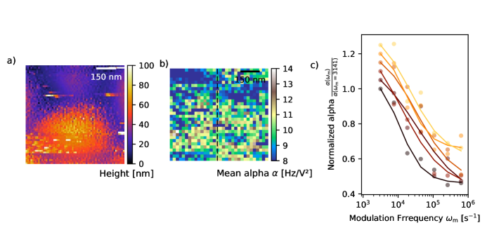
11 Supplementary figures summary
Figure 14 shows example frequency shift () \latinvs. applied tip voltage () and (b) amplitude () vs \latinvs. applied tip voltage () data for the data plotted in Figure 4 at selected light intensities for the \ceTiO2-substrate sample. Figure 16 shows representative AFM images of the four films studied in the manuscript. Figures 17 and 18 show the surface potential of each film \latinvs. light intensity and time, respectively. We note that the surface potential in each of these samples showed a distinct, non-trivial light-dependent and time-dependent behavior. Figure 19 shows that if below-bandgap illumination was used, there was no change in sample-induced dissipation, confirming that generation of free carriers is necessary to observe a light-induced change in sample conductivity. Figure 20 shows that the dissipation-recovery time constant for the \ceSnO2-substrate sample did not change in the measured temperature window.
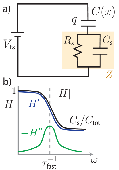
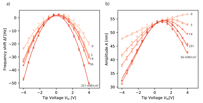
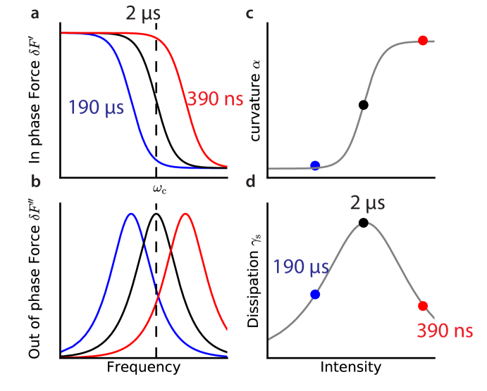
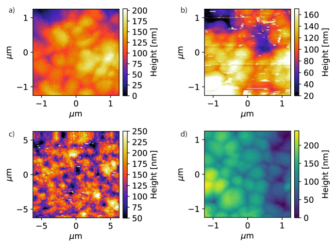
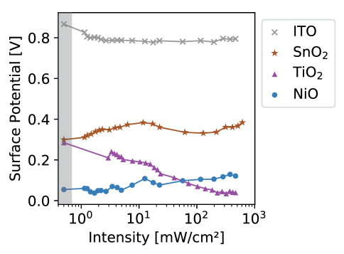
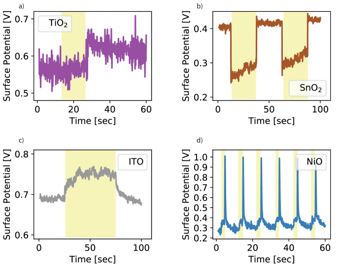
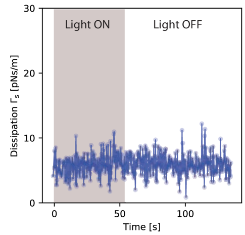
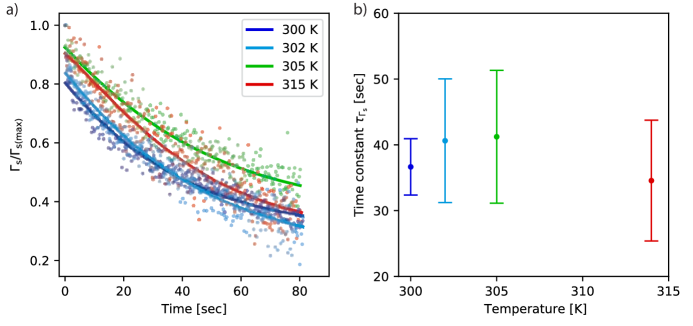
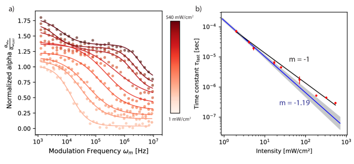
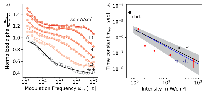
References
- 1 M. Labardi, M. Lucchesi, D. Prevosto, and S. Capaccioli, Broadband Local Dielectric Spectroscopy, Appl. Phys. Lett., 2016, 108, 182906, URL http://dx.doi.org/10.1063/1.4948767.
- 2 A. M. Tirmzi, R. P. Dwyer, T. Hanrath, and J. A. Marohn, Coupled Slow and Fast Charge Dynamics in Cesium Lead Bromide Perovskite, ACS Energy Lett., 2017, 2, 488 – 496, URL http://dx.doi.org/10.1021/acsenergylett.6b00722.
- 3 J. L. Luria Spectroscopic Characterization of Charge Generation and Trapping in Third-Generation Solar Cell Materials Using Wavelength- and Time-Resolved Electric Force Microscopy PhD thesis, Cornell University, Ithaca, New York, 2011, URL http://hdl.handle.net/1813/30762.
- 4 R. P. Dwyer, S. R. Nathan, and J. A. Marohn, Microsecond Photocapacitance Transients Observed Using a Charged Microcantilever as a Gated Mechanical Integrator, Sci. Adv., 2017, 3, e1602951, URL http://dx.doi.org/10.1126/sciadv.1602951.
- 5 D. Rugar, H. Mamin, and P. Guethner, Improved Fiber-Optic Interferometer for Atomic Force Microscopy, Appl. Phys. Lett., 1989, 55, 2588 – 2590, URL http://dx.doi.org/10.1063/1.101987.
- 6 E. M. Muller Electric Force Microscopy of Charge Trapping in Thin-Film Pentacene PhD thesis, Cornell University, Ithaca, New York, 2005.
- 7 S. M. Yazdanian, J. A. Marohn, and R. F. Loring, Dielectric Fluctuations in Force Microscopy: Noncontact friction and Frequency Jitter, J. Chem. Phys., 2008, 128, 224706, URL http://dx.doi.org/10.1063/1.2932254.
- 8 R. P. Dwyer and J. A. Marohn, The FreqDemod 0.2.1 Python package. Available for installation at https://pypi.python.org/pypi/FreqDemod. Documentation available at http://freqdemod.readthedocs.org. Source code available at https://github.com/JohnMarohn/FreqDemod., 2015.
- 9 L. M. Smieska Microscopic Studies of the Fate of Charges in Organic Semiconductors: Scanning Kelvin Probe Measurements of Charge Trapping, Transport, and Electric Fields in p- and n-type Devices PhD thesis, Cornell University, Ithaca, New York, 2015, URL http://hdl.handle.net/1813/40969.