Necessary conditions for out-of-plane lattice plasmons in nanoparticle arrays
Abstract
Out-of-plane lattice plasmons (OLPs) supported by metallic nanoparticle arrays are promising for diverse applications due to their remarkably narrow linewidths and significant enhancement of local fields. Here we investigate the necessary conditions for metallic nanoparticle arrays to achieve OLPs. Our results show that, besides the prerequisites of large height, oblique incidence, and TM polarization, which have been pointed out by the literature; the array period should be properly designed within a limited range, the dielectric environment should be homogeneous, and the height and the angle of incidence need to be optimized. We expect this work will advance the understanding and engineering of OLPs in metallic nanoparticle arrays and promote their applications in nanolasers, ultrasensitive biochemical sensors, and nonlinear optics.
1Institute of Photonics and Optical Science (IPOS), School of Physics, The University of Sydney, Sydney, New South Wales 2006, Australia
2Shenzhen Institutes of Advanced Technology, Chinese Academy of Sciences, Shenzhen 518055, Guangdong Province, China
*gy.li@siat.ac.cn
1 Introduction
Plasmonic nanostructures have attracted increasing attention because they can concentrate light in small regions and thus greatly enhance light-matter interactions. One of the simplest plasmonic structures is a single metallic nanoparticle, which can support a localized surface plasmon resonance (LSPR) with large local field enhancement [1]. However, LSPRs suffer from short plasmon lifetimes (2-10 fs) [2] and low quality factors () [3], which limits the local field intensity and the light-matter interaction enhancement. A powerful strategy to address this problem is to pattern nanoparticles in one- or two-dimensional arrays [4, 5, 6]. Due to strong coupling between neighboring nanoparticles, lattice plasmons supported by metallic nanoparticle arrays combine desirable photonic and plasmonic attributes, including suppressed radiative loss, high quality factor, and significant field enhancement over large volumes [4, 5, 6]. To date, most work has focused on in-plane lattice plasmons (ILPs) [7, 8, 9, 10, 11, 12], which are produced due to inter-particle coupling of in-plane LSPR oscillations. It has been demonstrated that a homogeneous dielectric environment is beneficial for achieving narrow linewidth, although narrow linewidth can still be observed in an asymmetric dielectric environment provided that the grating is properly designed [13, 12]. As a result, the effects of the array period, dielectric environment and nanoparticle dimensions on ILPs are well understood, and ILPs have already found attractive applications in nanolasers [14, 15], nonlinear optics [16, 17, 18], and ultrasensitive sensing [19, 20, 21].
Recently, Zhou and Odom demonstrated a new type of subradiant plasmon — out-of-plane lattice plasmon (OLP) [22], and found that it is a leaky surface Bloch mode [23]. Compared with ILPs, OLPs are shown to have easier tunability [22], lower thresholds for surface plasmon amplification [24], and much higher quality factors [25]. This is because OLPs have stronger inter-particle coupling [22, 25], which suppresses radiative decay, traps light in the plane of the array and strongly localizes fields around each nanoparticle [22]. In order to achieve strong OLPs, Zhou and Odom showed that the height of the nanoparticles should be large ( nm), and that the incident light should be oblique and TM polarized [22]. OLPs cannot be excited with TE polarized light because there is no out-of-plane electric field component of the incident light [22]. In addition, Huttunen et al. found that hexagonal arrays are better than square arrays [25]. However, the effects of the array period and the dielectric environment on OLPs have not been fully understood yet, hampering the engineering and application of OLPs. For example, although all the above work on OLPs [22, 23, 24, 25] adopted homogeneous dielectric environments, in a recent review Kravets et al. surmised that for OLPs, the refractive index mismatch between substrate and superstrate is less important since the electric fields associated with the interaction between neighboring particles are primarily in the superstrate [6].
Here, we report the necessary conditions for metallic nanoparticle arrays to achieve OLPs. We will systematically investigate the effects of key parameters on OLPs, including the array period and the dielectric environment, as well as the nanoparticle height and the angle of incidence. We will examine whether OLPs can be supported in a highly asymmetric dielectric environment. We will also provide intuitive theoretical explanations to our simulation results, unveiling the roles of different parameters. We expect this work will deepen our understanding of OLPs and bring them closer to practical applications in nanolasers, nonlinear optics and sensing.
2 Simulation setup
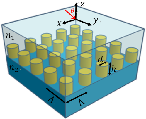
Figure 1 illustrates the metallic nanoparticles patterned in a square array with period in both the and directions. Each nanoparticle is cylindrical with height and diameter . The nanoparticle array is fabricated on a dielectric substrate with refractive index , and is later covered by a thick-enough superstrate with refractive index . The structure is illuminated by plane waves at oblique incidence, the plane of which is aligned with the axis of the grating (the plane). Note that here is the angle of incidence in air so as to be consistent with the incidence angle in measurements [22].
In order to calculate the reflection, transmission and absorption spectra of such a system, we adopt the rigorous coupled wave analysis (RCWA) method, which is very powerful for the analysis and design of periodic structures such as gratings and metamaterials. Calculations were performed using the open-source RCWA software RETICOLO, which was developed by Hugonin and Lalanne [26]. In order to plot the fields at specific wavelengths, we used the commercial finite-difference time-domain (FDTD) software Lumerical FDTD Solutions.
With the calculated total reflection and total transmission , we can then calculate the scattering, extinction and absorption cross sections defined as:
| (1) | ||||
For all the calculations in this work, we use gold as the material of metallic nanoparticles with refractive index data in the visible and near-infrared regime tabulated in [27]. Unless otherwise specified, the incident light is TM polarized with the magnetic field parallel to the direction, the metallic nanoparticles have a height of nm, a diameter of nm, a period of nm, the angle of incidence is , and the dielectric environment is homogeneous with .
3 Results and discussion
3.1 Effect of array period
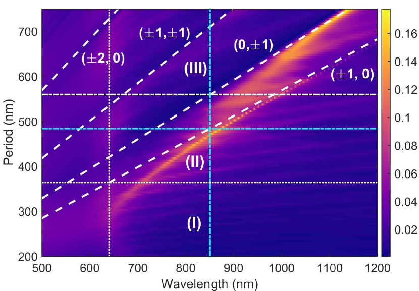
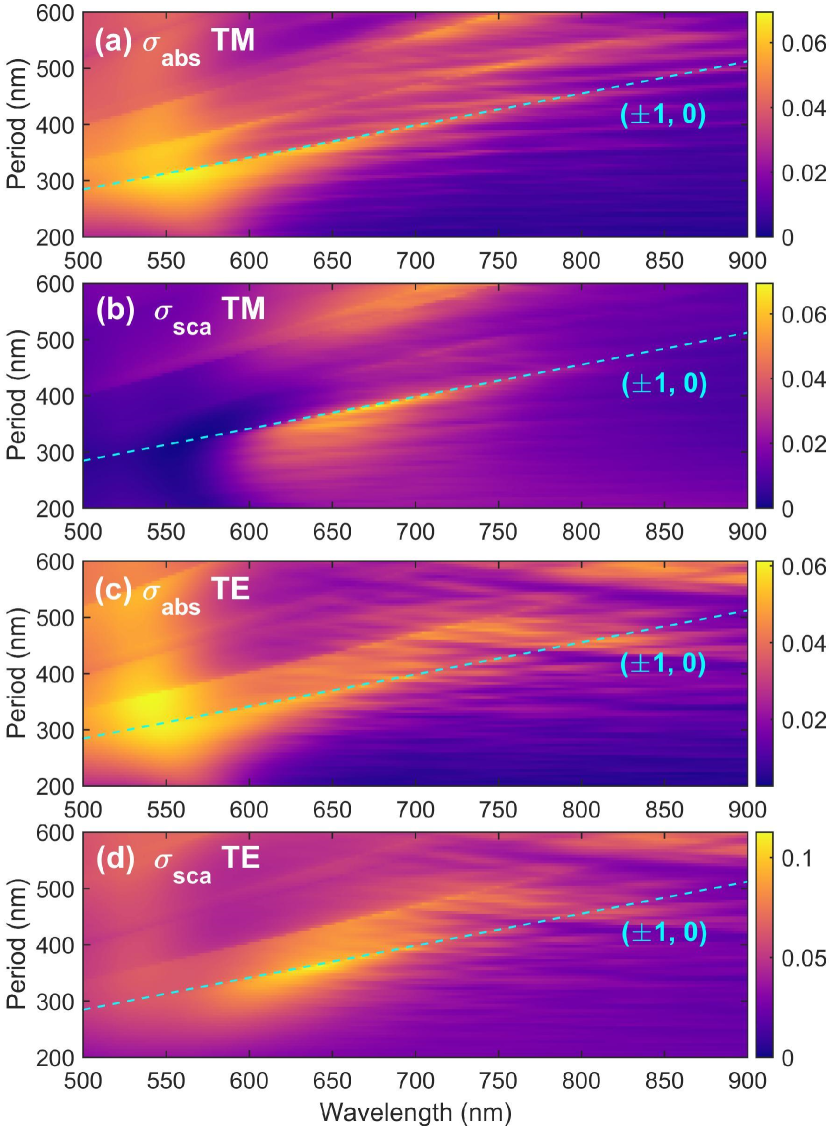
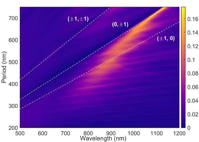
We first investigate the effect of the array period on OLPs, which has not been discussed in the literature yet. Figure 2 shows the calculated absorption cross section as a function of the wavelength and the period. To understand the behavior, we also superimpose the positions of the Rayleigh anomaly (RA), which is associated with light diffracted parallel to the in-plane surface. RAs occur when the period and wavelength satisfy [28]
| (2) |
where integer index pairs denote the order of RAs.
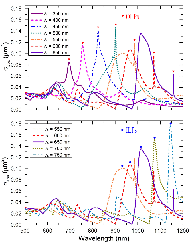
We find that OLPs with extremely narrow linewidth and large absorption cross section occur only when the period is properly selected from a limited range, , which is denoted as Region (II) in Fig. 2. As the period increases within this region, the absorption cross section of OLPs first increases and then decreases, and the linewidth keeps narrowing down. The maximum absorption cross section is achieved when . In this case, out-of-plane dipolar interactions between nanoparticles are well coupled with the in-plane LSPR of individual gold nanoparticles (located around 850 nm [22]), leading to a remarkable narrow absorption peak near . Fig. 3 shows that when the array period is tuned away, the out-of-plane diffraction spectrally deviates from the in-plane LSPR, resulting in reduced absorption cross section. The lower diffraction edge can be roughly determined by the out-of-plane LSPR of individual nanoparticles ( nm) through , corresponding to nm, as shown by the white horizontal dotted line in Fig. 2. The upper diffraction edge can be approximately decided by , corresponding to nm, as shown by the white horizontal dashed line in Fig. 2.
As the period further increases to nm, which is denoted as Region (III) in Fig. 2, ILPs with much wider linewidth appear, and show increasing absorption cross section and decreasing linewidth, as shown by Figs. 2 and 3. OLPs gradually disappear, whereas ILPs gradually dominate and converge to the RA. Note that the resonant wavelength of ILPs depends on the period, and the linewidths are much smaller than that of the in-plane LSPR of individual nanoparticles ( nm [22]).
For very small periods in Region (I) in Fig. 2, i.e., , the absorption cross section is very weak although broadband. For such small periods that are close to the diameter of the cylindrical gold nanoparticle, the plasmonic structure behaves like a bulk metal with small dielectric inclusions [29]. In this scenario, the near-field coupling between adjacent nanoparticles is very strong, resulting in enhanced localized gap plasmons.
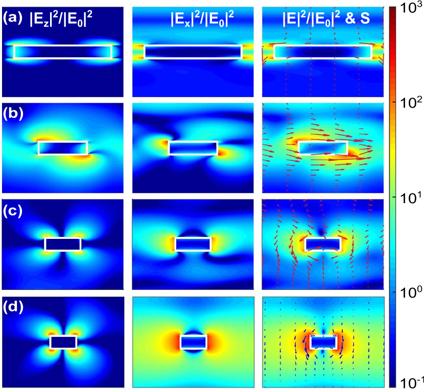
Figure 4(a) shows that the electric field of the localized plasmon mode for nm and nm is dominated by the component, and is mainly confined to the gap due to strong near-field coupling between neighboring nanoparticles. Fig. 4(b) shows that the electric field of the OLP for nm and nm is dominated by its out-of-plane component . The Poynting vector map shows that the energy flux propagates along and is concentrated above and below the plane of the two-dimensional nanoparticle array. Therefore, the out-of-plane lattice plasmon mode is an electromagnetic wave that propagates in-plane but polarizes out-of-plane. Fig. 4(c) shows that the electric field of the ILP is dominated by its in-plane component , and the energy flux circulates around the nanoparticles. As the period increases from 550 nm to 750 nm, as shown by Fig. 4(c)(d), the coupling between in-plane nanoparticle dipolar moments is greatly enhanced, resulting in increased absorption cross section and narrowed linewidth of the ILP (see Fig. 3).
| Period | Effect |
|---|---|
| Near-field coupling | |
| OLPs | |
| ILPs |
Therefore, given the individual metallic nanoparticles, the array period determines both the strength and the spectral position of the absorption cross section of the OLPs. Table 1 summarizes the dominant effects for different periods in Regions (I)-(III) in Fig. 2. For , the inter-particle gap is small enough that the array LSPR dominates; for , ILPs become dominant; only for periods that are properly designed within , OLPs with extremely narrow linewidths and large absorption cross sections can be observed. The strongest OLP is achieved when the array period is around , which satisfies .
While we mostly concentrated on the TM polarization, which has the out-of-plane electric component () of the incident light, we also found that TE polarized incident light, which has only the in-plane electric component (), cannot excite OLPs, consistent with the results obtained by Zhou and Odom [22].
3.2 Effect of dielectric environment
Previously, we have taken the dielectric environment to be homogeneous, which simplifies theoretical analysis and simulations. In experiments, however, inhomogeneous dielectric environments are easier to implement since the refractive indices of the superstrate and of the substrate are usually different. It is known that the optimal ILPs is achieved when the superstrate and substrate are index matched [11, 12, 5]. Here we show that a homogeneous dielectric environment is also vital for achieving OLPs.

We consider a large refractive index difference between the superstrate and the substrate: (air) and . For such an inhomogeneous dielectric environment and TM polarized oblique incidence, Fig. 5(a)(b) shows that when the period is properly selected (around 380 nm, also around the order RA line), both the absorption and the scattering cross section spectra show a narrow peak. The resulting extinction cross section spectra (), as shown in Fig. 6(a) shows a peak at nm with a linewdith of nm, corresponding to a quality factor of 29. This quality factor is larger than that obtained for a 200 nm tall gold nanoparticle array in a asymmetric air/glass environment (), as reported by Thackray et al. [13].
In order to understand such a narrow collective plasmon resonance, which was attributed to the out-of-plane coupling of the localized surface plasmon resonances of the individual nanostructures [13], we calculated the corresponding electric fields and the Poynting vector map, as shown in Fig. 6(b). The results show that the in-plane dipole interactions dominate, the circulating energy flows around the nanoparticle, and the energy flux propagates along the direction and is concentrated below the nanoparticle array. This suggests that this collective plasmon resonance is an ILP rather than an OLP. To further confirm that an ILP is excited in this scenario, we also calculated the results for the TE polarization, as shown in Fig. 5(c)(d). Comparing Figs. 5 and 6(a), it is evident that narrow collective plasmon resonances with similar linewidths can be excited for both TE and TM polarization. Additionally, we find that the interactions betsween neighboring particles are primarily in the substrate, rather than in the superstrate. These results are opposite to the hypothesis by Kravets et al., who surmised that for OLPs, which are supported in tall nanoparticles and are excited under oblique incidence, the refractive index mismatch between substrate and superstrate is less important since the electric fields associated with the interactions between neighboring particles are primarily in the superstrate [6].
Therefore, our results suggest that OLPs require homogeneous dielectric environment even more than ILPs. It has been shown that ILPs supported by short (usually 50 nm tall) metal nanoparticle arrays prefer homogeneous dielectric environments [12], and ILPs supported by tall (for example 200 nm tall) metal nanoparticle arrays can have narrow linewidths for an environment as asymmetric as the air/glass environment [13]. This is because for inhomogeneous dielectric environments, the electric field distribution is highly asymmetric and most of the energy is confined to the high-index substrate; in-plane dipolar interactions can interact strongly through the RA in the substrate, as shown by Figs. 5 and 6(b); however, out-of-plane dipolar interactions are mainly in the superstrate (air in this case), leading to very weak out-of-plane inter-particle interactions due to the weak field in the superstrate.
3.3 Effects of height and incidence angle
Zhou and Odom found that OLPs can be pronounced only for nm given , and that the absorption cross section is optimized for given nm [22]. This finding helps to understand the fact that most work has been focused on ILPs, and has failed to observe OLPs: nanoparticles that are easy to fabricate are too short (usually nm), or incidence that is easy to implement in experiments is normal incidence (i.e., ). Indeed, for short nanoparticles with nm, we explored all the other parameters and found that OLPs are too weak to be observed, but ILPs still exist and eventually converge to the order RA, as shown by Fig. 7. This is because the height only affects the out-of-plane oscillation [22], whereas the in-plane oscillation mainly depends on the nanoparticle diameter and the period [12].
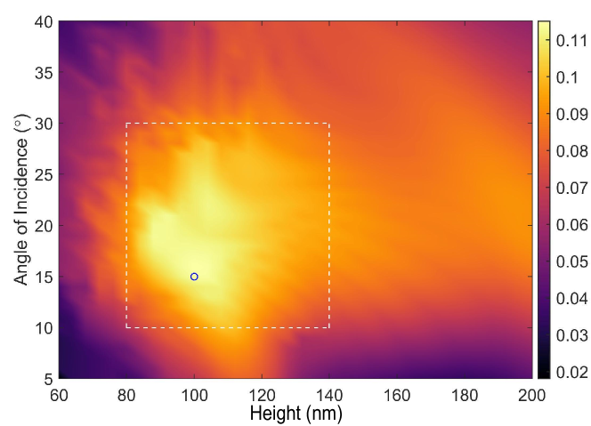
Here we systematically study the effects of both the nanoparticle height and the angle of incidence , both of which vary simultaneously (on the contrary, the discussion was performed by varying only one parameter given the other one in [22]). Figure 8 shows the peak absorption cross section as functions of both and . Here denotes the peak value of the spectrum, i.e., . Results show that a large absorption cross section can be achieved only for a small range of nanoparticle heights and angles of incidence: , and , as indicated by the dashed rectangle in the figure. The optimal nanoparticle height and angle of incidence are around and , consistent with Zhou and Odom [22].
The optimal range for nanoparticle height and angle of incidence can be understood as follows. For too small a , the out-of-plane electric field component is too weak to excite out-of-plane dipoles. As increases, the out-of-plane electric field component increases, leading to larger . However, if is too large, the out-of-plane lattice plasmon spectrally shifts beyond the broad in-plane lattice plasmon [22]. On the other hand, nanoparticles that are too short cannot support out-of-plane dipoles, resulting in small originating from ILPs. As the nanoparticle height increases, out-of-plane dipoles and OLPs can be supported, leading to larger . However, if is too large, the out-of-plane dipole suffers from high Ohmic loss due to the long nanoparticle, which limits the inter-particle coupling and reduces of OLPs. Therefore, there is a compromise for both the angle of incidence and the nanoparticle height. Similar phenomena can also be observed and explained similarly for other periods in Regime (II) in Fig. 2.
4 Conclusion
In conclusion, we have investigated the effects of key parameters of metallic nanoparticle arrays, including the array period, the dielectric environment, the nanoparticle height and the angle of incidence, on OLPs. By doing this, we have managed to clarify the necessary conditions for achieving strong OLPs. Our results have shown that in addition to the oblique incidence, the TM polarization, and the large nanoparticle height, which have been pointed out by the literature; other necessary conditions include a properly designed array period within a limited range of , a homogeneous dielectric environment, and optimized pair of the nanoparticle height and the angle of incidence. We also clarify that for tall metal nanoparticles in an environment as asymmetric as air/polymer (with a large refractive index difference 1.0/1.52) environment, it is the ILP rather than the OLP that can be excited. We expect these findings will advance the understanding and the design of OLPs, as well of ILPs in tall metal nanopartical array, and promote OLPs with extremely narrow linewidth and high quality factor for applications in nanolasers, nonlinear optics and ultrasensitive sensing.
Funding
Key Research Items from the Ministry of Science and Technology of China (Grant No. 2016YFC1400701); State Key Laboratory of Advanced Optical Communication Systems Networks, China (Grant No. 2019GZKF2).
References
- [1] P. Mühlschlegel, H.-J. Eisler, O. J. F. Martin, B. Hecht, and D. W. Pohl. Resonant optical antennas. Science, 308:1607–1609, 2005.
- [2] S. Link and M. A. El-Sayed. Spectral properties and relaxation dynamics of surface plasmon electronic oscillations in gold and silver nanodots and nanorods. J. Phys. Chem. B, 103:8410–8426, 1999.
- [3] Govinda Lilley, Manuel Messner, and Karl Unterrainer. Improving the quality factor of the localized surface plasmon resonance. Opt. Mater. Express, 5:2112–2120, 2015.
- [4] Michael B. Ross, Chad A. Mirkin, and George C. Schatz. Optical properties of one-, two-, and three-dimensional arrays of plasmonic nanostructures. J. Phys. Chem. C, 120:816–830, 2016.
- [5] Weijia Wang, Mohammad Ramezani, A. I. Väkeväinen, P. Törmä, J. G. Rivas, and T. W. Odom. The rich photonic world of plasmonic nanoparticle arrays. Mater. Today, 21:303–314, 2018.
- [6] V. G. Kravets, A. V. Kabashin, W. L. Barnes, and A. N. Grigorenko. Plasmonic surface lattice resonances: A review of properties and applications. Chem. Rev., 118:5912–5951, 2018.
- [7] Shengli Zou, Nicolas Janel, and George C. Schatz. Silver nanoparticle array structures that produce remarkably narrow plasmon lineshapes. J. Chem. Phys., 120:10871, 2004.
- [8] V. G. Kravets, F. Schedin, and A. N. Grigorenko. Extremely narrow plasmon resonances based on diffraction coupling of localized plasmons in arrays of metallic nanoparticles. Phys. Rev. Lett., 101:087403, 2008.
- [9] B. Auguié and W. L. Barnes. Collective resonances in gold nanoparticle arrays. Phys. Rev. Lett., 101:143902, 2008.
- [10] Yizhuo Chu, Ethan Schonbrun, Tian Yang, and Kenneth B. Crozier. Experimental observation of narrow surface plasmon resonances in gold nanoparticle arrays. Appl. Phys. Lett., 93:181108, 2008.
- [11] B. Auguié, X. M. Bendana, W. L. Barnes, and F. J. G. de Abajo. Diffractive arrays of gold nanoparticles near an interface: Critical role of the substrate. Phys. Rev. B, 82:155447, 2010.
- [12] D. Khlopin, F. Laux, William P. Wardley, J. Martin, Gregory A. Wurtz, J. Plain, Nicolas Bonod, A. V. Zayats, Wayne Dickson, and Davy Gérard. Lattice modes and plasmonic linewidth engineering in gold and aluminum nanoparticle arrays. J. Opt. Soc. Am. B, 34:691–700, 2017.
- [13] Benjamin D. Thackray, Vasyl G. Kravets, Fred Schedin, Gregory Auton, Philip A. Thomas, and Alexander N. Grigorenko. Narrow collective plasmon resonances in nanostructure arrays observed at normal light incidence for simplified sensing in asymmetric air and water environments. ACS Photon., 1:1116–1126, 2014.
- [14] Wei Zhou, Montacer Dridi, Jae Yong Suh, Chul Hoon Kim, Dick T. Co, Michael R. Wasielewski, George C. Schatz, and Teri W. Odom. Lasing action in strongly coupled plasmonic nanocavity arrays. Nat. Nanotechnol., 8:506–511, 2013.
- [15] Ankun Yang, Thang B. Hoang, Montacer Dridi, Claire Deeb, Maiken H. Mikkelsen, George C. Schatz, and Teri W. Odom. Real-time tunable lasing from plasmonic nanocavity arrays. Nat. Commun., 6:6939, 2015.
- [16] R. Czaplicki, A. Kiviniemi, J. Laukkanen, J. Lehtolahti, M. Kuittinen, and M. Kauranen. Surface lattice resonances in second-harmonic generation from metasurfaces. Opt. Lett., 41:2684–2687, 2016.
- [17] Robert Czaplicki, Antti Kiviniemi, Mikko J. Huttunen, Xiaorun Zang, Timo Stolt, Ismo Vartiainen, J. Butet, Markku Kuittinen, Olivier J. F. Martin, and Martti Kauranen. Less is more: Enhancement of second-harmonic generation from metasurfaces by reduced nanoparticle density. Nano Lett., 18:7709–7714, 2018.
- [18] Mohammad Ramezani, Quynh Le-Van, and Alexei Halpin. Nonlinear emission of molecular ensembles strongly coupled to plasmonic lattices with structural imperfections. Phys. Rev. Lett., 121:243904, 2018.
- [19] Peter Offermans, Martijn C. Schaafsma, Said R. K. Rodriguez, Yichen Zhang, Mercedes Crego-Calama, Sywert H. Brongersma, and Jaime G. Rivas. Universal scaling of the figure of merit of plasmonic sensors. ACS Nano, 5:5151–5157, 2011.
- [20] Jing Chen, Wenfang Fan, Tao Zhang, Chaojun Tang, Xingyu Chen, Jingjing Wu, Danyang Li, and Ying Yu. Engineering the magnetic plasmon resonances of metamaterials for high-quality sensing. Opt. Express, 25:3675–3681, 2017.
- [21] Artem Danilov, Gleb Tselikov, Fan Wu, Vasyl G. Kravets, Igor Ozerov, Frederic Bedu, Alexander N. Grigorenko, and Andrei V. Kabashin. Ultra-narrow surface lattice resonances in plasmonic metamaterial arrays for biosensing applications. Biosens. Bioelectron., 104:102–112, 2018.
- [22] W. Zhou and T. W. Odom. Tunable subradiant lattice plasmons by out-of-plane dipolar interactions. Nature Nanotechnol., 6:423–427, 2011.
- [23] Wei Zhou, Yi Hua, Mark D. Huntington, and Teri W. Odom. Delocalized lattice plasmon resonances show dispersive quality factors. J. Phys. Chem. Lett., 3:1381–1385, 2012.
- [24] Pei Ding, Genwang Cai, Junqiao Wang, Jinna He, Chunzhen Fan, Xiaomin Liu, and Erjun Liang. Low-threshold resonance amplification of out-of-plane lattice plasmons in active plasmonic nanoparticle arrays. J. Opt., 16:065003, 2014.
- [25] M. J. Huttunen, Ksenia Dolgaleva, P. Törmä, and Robert W. Boyd. Ultra-strong polarization dependence of surface lattice resonances with out-of-plane plasmon oscillations. Opt. Express, 24:28279–28289, 2016.
- [26] J. P. Hugonin and P. Lalanne. Reticolo software for grating analysis. Institut d’Optique, Orsay, France, 2005.
- [27] P. B. Johnson and R. W. Christy. Optical constants of the noble metals. Phys. Rev. B, 6:4370–4379, 1972.
- [28] H. Gao, J. M. McMahon, M. H. Lee, J. Henzie, S. K. Gray, G. C. Schatz, and T. W. Odom. Rayleigh anomaly-surface plasmon polariton resonances in palladium and gold subwavelength hole arrays. Opt. Express, 17:2334–2340, 2009.
- [29] Linda Gunnarsson, Tomas Rindzevicius, Juris Prikulis, Bengt Kasemo, Mikael Käll, Shengli Zou, and George C Schatz. Confined plasmons in nanofabricated single silver particle pairs: experimental observations of strong interparticle interactions. The Journal of Physical Chemistry B, 109:1079–1087, 2005.