Characterization and Modeling of 0.18m CMOS Technology at sub-Kelvin Temperature
Abstract
Previous cryogenic electronics studies are most above 4.2K. In this paper we present the cryogenic characterization of a 0.18m standard bulk CMOS technology(1.8V and 5V) at sub-kelvin temperature around 270mK. PMOS and NMOS devices with different width to length ratios(W/L) are tested and characterized under various bias conditions at temperatures from 300K to 270mK. It is shown that the 0.18m standard bulk CMOS technology is still working at sub-kelvin temperature. The kink effect and current overshoot phenomenon are observed at sub-kelvin temperature. Especially, current overshoot phenomenon in PMOS devices at sub-kelvin temperature is shown for the first time. The transfer characteristics of large and thin-oxide devices at sub-kelvin temperature are modeled using the simplified EKV model. This work facilitates the CMOS circuits design and the integration of CMOS circuits with silicon-based quantum chips at extremely low temperatures.
Index Terms:
Cryogenic CMOS, characterization, modeling, kink effect, current overshoot, sub-kelvin temperature.I Introduction
Cryogenic CMOS(cryo-CMOS) has been researched in recent years due to the rise of quantum chip and quantum computer research[1][2]. CMOS circuits integrated with quantum bits on the same substrate or standalone CMOS circuits working at extremely low temperatures can improve the scalability of quantum chips, system integration and performance[3][4]. However, cryo-CMOS circuits face several changes such as refrigeration power, interconnection and device modeling.
The applicable temperature for BSIM3 or BSIM4 model is from - 40℃ to 125 ℃ in general. The characteristics of MOSFET devices change due to freeze-out effect at low temperatures. At present, CMOS technologies ranging from 0.35m to 28nm have been characterized and modeled at the liquid nitrogen temperature(77K) and the liquid helium temperature(4.2K)[5, 6, 7]. However, the characteristic testing and modeling at the sub-kelvin temperature are lacking[8].
The paper contains the characteristics of 0.18m MOSFET devices, kink effect and current overshoot phenomenon of MOSFET at sub-kelvin temperature. The EKV model for transfer characteristics of large size devices is provided, which can be used for estimating power consumption of devices and the simulation of CMOS circuits design at sub-kelvin temperature.
II Cryogenic Measurement Setup
Measurements of CMOS transistors were performed with two different gate oxide thicknesses(TOX) and a wide range of device sizes at around 270mK, as shown in Table I. The tested chip and chip-carrier were connected with Al-wire bonding. The 3He refrigerator was used to cool devices. The devices under test(DUT) were put into the dual in-line package(DIP) socket at the bottom of the refrigerator and connected to BNC connectors at the top of the refrigerator via cables. An internal vacuum chamber was built around the sample, and the sample was inserted into the cryostat to cool down to around 270mK.All MOSFET electrical measurements were performed using the Keysight B1500A semiconductor device analyzer. The interconnection between the DUT and B1500A was realized through BNC cables and BNC Triax to BNC adapters.
| Technology | SMIC 0.18m Bulk CMOS 1P6M Process | |||
|---|---|---|---|---|
| Voltage and TOX | 1.8V Thin | 5V Thick | ||
| Type | NMOS | PMOS | NMOS | PMOS |
| W/L[m/ m] | 10/10 | 10/10 | 10/10 | 10/10 |
| 10/0.6 | 10/0.6 | 10/2 | 10/2 | |
| 10/0.2 | 10/0.18 | 10/0.65 | 10/0.5 | |
| 10/0.18 | 10/0.16 | 10/0.5 | 10/0.45 | |
| 10/0.16 | 0.3/0.6 | |||
Testing of the characteristics at around 270mK should limit the power of devices, limited by the cooling power. For 1.8V MOSFET, transfer characteristics in linear and saturation regions for different substrate bias voltages were measured on various devices in Table I; output characteristics in zero substrate bias and reverse bias voltage for different gate voltages were measured. For 5V MOSFET, bias voltages changed. Characteristics in other bias voltages were also measured at around 270mK. In addition to the above measurements, the output characteristics were measured which were in different hold-time and delay time.
III Characterization
III-A Transfer Characteristics
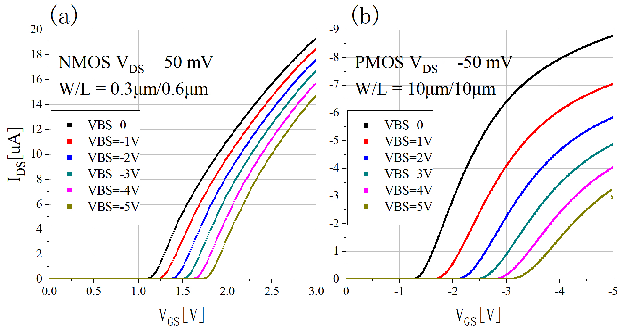
Fig.1 shows the transfer characteristics of large and small thin TOX MOSFET devices. Fig.2 shows the transfer characteristics of the thick TOX NMOS (W/L=0.3m/0.6m) and PMOS (W/L =10m/10m) in liner region. The drain current is still depending on the and W/L. The threshold voltage changes with substrate bias voltage. Transfer characteristics are similar to the usual results for MOSFET. Fig. 1(a,b) give transfer characteristics of the large NMOS device at sub-kelvin temperature. For the small NMOS device in Fig.1(c,d), the decreases rapidly because of drain induced barrier lowering(DIBL) effect[9][10]. The DIBL effect is also shown in Fig.1(g,h).
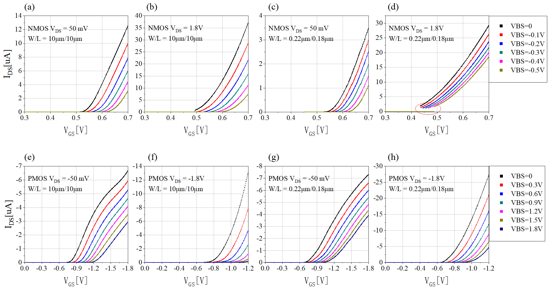
An abnormal phenomenon about current step is shown in Fig.1(d); for in Fig.1(b), we can observe current step phenomenon also. When the gate to source voltage reaches , suddenly changes into microamperes(A) current. The abnormal phenomenon prohibits the use of small NMOS devices in saturation region for extremely low-power circuits.
III-B Output Characteristics and Kink Effect
We have plotted in Fig.3(a-d) output characteristics of thin and thick TOX MOSFET devices, obtained at sub-kelvin temperature. We choose the current-limiting method to keep the temperature stable. These curves (forward and backward scan) in Fig.3 show the kink effect. The kink effect can occur on MOSFET devices at sub-kelvin temperatures when the becomes sufficiently high[11]. For bulk silicon NMOS devices at low temperatures, channel electron can gain enough energy and produce electron-hole pairs by impact ionization when the is higher than a certain value. The electrons pass through the channel to the drain, and the holes migrate towards the floating substrate. The floating substrate potential increases due to the accumulation of holes, until the substrate-source junction forms forward bias[11][12]. The reduces with the increase of substrate potential. As the increases, the decreases, resulting in the increase of drain-source current .
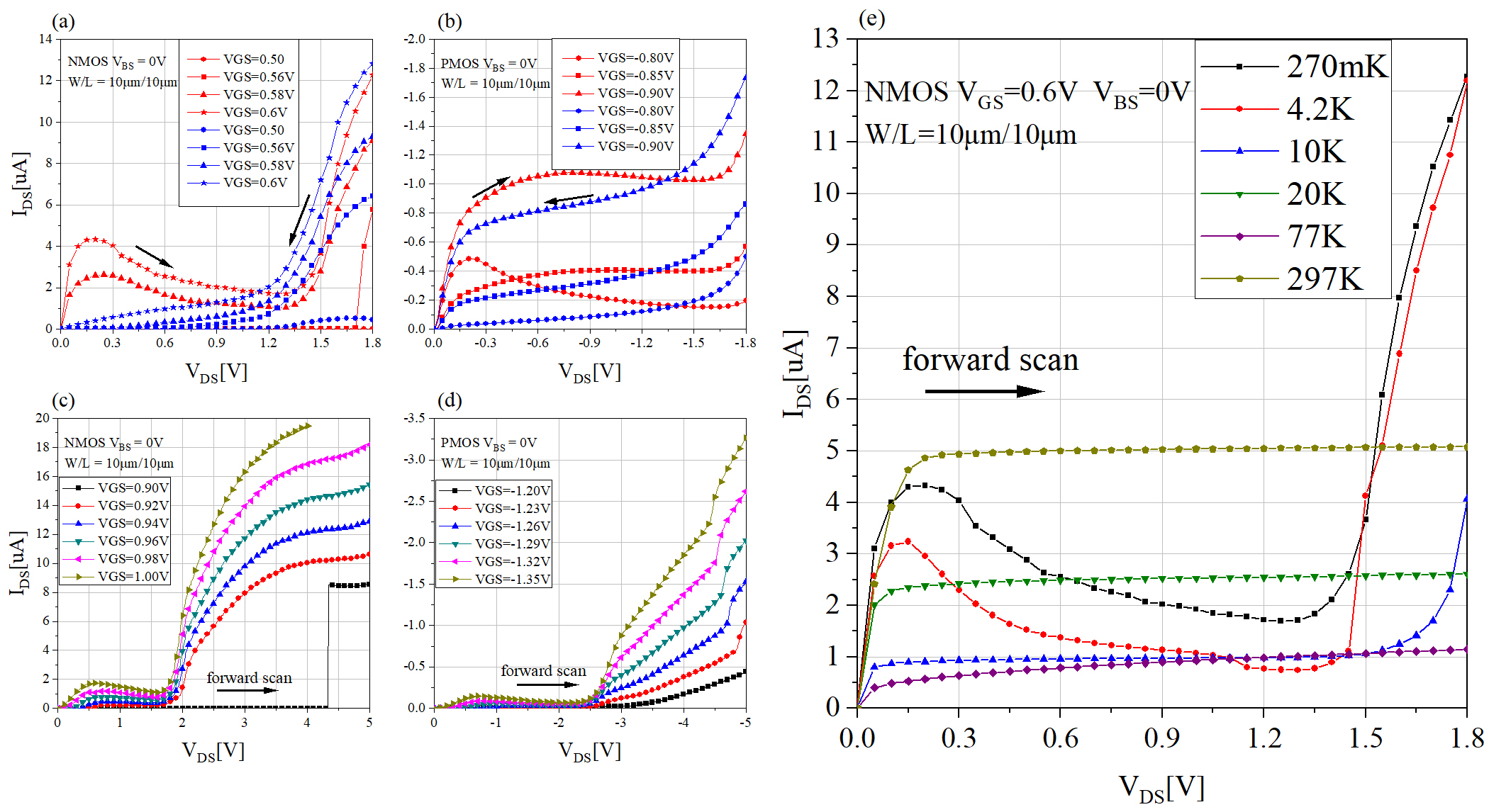
Compared to PMOS devices, the kink effect in NMOS devices appears at lower voltage, and the amplification of NMOS is bigger. Considering to the higher impact-ionization multiplication factor of electrons compared to holes, NMOS devices are more affected at sub-kelvin temperature compared to PMOS devices[13].
Besides, we observed the current overshoot phenomenon in Fig.3 when the scan model is forward scan. For forward scan results of thin TOX PMOS, the current overshoot occurs obviously while the test begins. The kink effect and current overshoot phenomenon at cryogenic temperatures are related to varying with . As shown in Fig.3(e), the kink effect and current overshoot phenomenon attenuate and disappear with the temperature increasing.
III-C Current Overshoot and Discussion
The current overshoot phenomenon occurred in Fig.3(e) at temperatures below 10K other than 15K[14]. This phenomenon is related to the charge state of traps in the Si/SiO2 interface. The Si/SiO2 interface traps are silicon dangling-bonds at the interface. In the case of on state NMOS devices (forward scan), it can be seen that positive charging of traps leading to the noticeable increase of the current at the beginning of curves in Fig.4(a). The decreases in the liner region for NMOS devices owing to positive charge trapped in the interface traps. When is sufficiently high after reaching the pinch-off point, the trapped charges in the interface can be released at sub-kelvin temperature[14]. The increases and the amplitude of curves decreases in the saturation region as the increases, as shown in Fig.4(a,b).
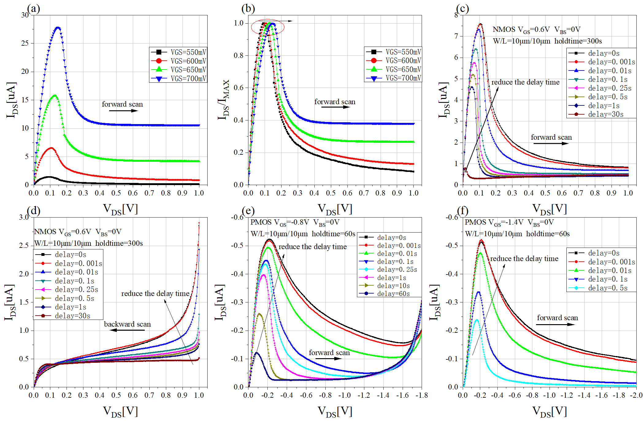
We measured the current overshoot with various delay time and two scan models. In Fig.4(c), the maximum amplitude of curves is 7.59A for 0 delay time, and the peak value decreases when the scan delay time increases. Predictably, the peak will disappear on the sufficient scan delay time. We do not observe the current overshoot in Fig.4(d), plotted results with backward scan model. For PMOS devices, the current overshoot phenomenon also occurred at sub-kelvin temperatures in Fig.4(e,f). The relation between the current overshoot phenomenon and the scan delay time implies the charge state of traps in the Si/SiO2 interface[14][8].
IV Modeling
IV-A EKV Model for Large Devices
The EKV MOSFET model is applicable to MOSFET devices in low-voltage and low-current applications[15]. And this model is compact and accurate with a few parameters[16][17]. The output characteristics of MOFET devices are abnormal at sub-kelvin temperature because of kink effect and current overshoot, and the data of thick TOX large devices is insufficient by the limitation of the cooling power. Given this, we choose the EKV 2.6 model to describe transfer characteristics of thin TOX large MOSFET devices. For large MOSFET devices, the intrinsic model parameters in Table II can describe transfer characteristics accurately, and the short and narrow channel effects are ignored. The value of parameters in Table II is for thin TOX PMOS devices.
| Name(unit) | Description | Value |
|---|---|---|
| TOX() | oxide thickness | 4.27e-009 |
| XJ() | junction depth | 1.6e-007 |
| DW() | channel width correction | -1.6e-008 |
| DL() | channel length correction | 7.6e-008 |
| NSUB() | channel doping | 1.0196e+017 |
| UCRIT() | longitudinal critical field | 2.0e+6 |
| VTO() | nominal threshold voltage | - |
| KP() | transconductance parameter | - |
| GAMMA() | body effect parameter | - |
| THETA() | mobility reduction coefficient | - |
Parameters of TOX, XJ, DW, DL, and NSUB are from BSIM4 model[18], and the parameter(UCRIT) can be set as default. The value of PHI(bulk Fermi potential) parameter is calculated with NSUB parameter. The value of is -272.88K(270mK), which is the nominal temperature of model parameters. We ignore the intrinsic parameters temperature dependence in EKV model because is set as 270mK equal to test temperature. Equations of interest are presented below[17][19][20].
| (1) |
where is intrinsic carrier concentration,
| (2) |
The expression of is
| (3) |
is the forward current and is the reverse current.
| (4) |
where the specific current
| (5) |
Considering the mobility reduction due to vertical field,
| (6) |
where is the pinch-off voltage for large devices.

| Region | liner | saturation |
|---|---|---|
| VTO() | 0.5208 | 0.46403 |
| GAMMA() | 0.50534 | 0.6024 |
| KP() | 0.0017217 | 0.0017958 |
| THETA() | 0.462 | 0.31198 |
| RMS(%) | 1.05 | 0.19 |
| Region | liner | saturation |
|---|---|---|
| VTO() | -0.7676 | -0.74 |
| GAMMA() | 0.66736 | 0.675 |
| KP() | 0.00018393 | 0.0001806 |
| THETA() | 0.32242 | 0.37118 |
| RMS(%) | 1.52 | 0.38 |
IV-B Parameters Extraction and Modeling
The parameters extraction is performed by BSIMProPlus with semi-empirical methods. We import the test data of thin TOX large MOEFET devices into the software and set value of TOX, XJ etc. The degree of agreement(described as RMS Error) between the simulation data and the test data changes with VTO, KP, GAMMA and THETA. After these parameters have been adjusted properly, the RMS Error declines to less than 5% (Fig.5).
The value of VTO in Table III and Table IV decreases from liner region to saturation region, which means the of large devices varies with operating modes. The explanation of the kink effect is validated. Comparing the value of parameters in liner region with the value of parameters in saturation region, the numerical difference of NMOS is greater than PMOS. It is proved that NMOS devices are more affected at sub-kelvin temperature compared to PMOS devices.
V Conclusion
The SMIC 0.18m bulk CMOS technology is tested and characterized at sub-kelvin temperature. It is demonstrated that MOSFET devices are still operating at sub-kelvin temperature. The kink effect and current overshoot phenomenon have been shown and explained. The EKV2.6 library with parameters extracted from transfer characteristics of thin TOX large devices at sub-kelvin temperature. The obtained results have proven the EKV2.6 library extracted is suited to describe transfer characteristics of thin TOX large devices at 270mK. This work contributes to research on characteristics of devices and cryogenic CMOS circuits design for quantum chips.
Acknowledgment
The authors would like to thank SMIC for devices fabrication and software support.
References
- [1] B. Patra, R. M. Incandela, J. P. G. van Dijk, H. A. R. Homulle, L. Song, M. Shahmohammadi, R. B. Staszewski, A. Vladimirescu, M. Babaie, F. Sebastiano, and E. Charbon, “Cryo-CMOS circuits and systems for quantum computing applications,” IEEE Journal of Solid-State Circuits, vol. 53, no. 1, pp. 309–321, Jan 2018.
- [2] F. Sebastiano, H. Homulle, B. Patra, R. Incandela, J. van Dijk, L. Song, M. Babaie, A. Vladimirescu, and E. Charbon, “Cryo-CMOS electronic control for scalable quantum computing: Invited,” in Proceedings of the 54th Annual Design Automation Conference 2017, ser. DAC ’17. New York, NY, USA: ACM, 2017, pp. 13:1–13:6. [Online]. Available: http://doi.acm.org/10.1145/3061639.3072948
- [3] L. Hutin, B. Bertrand, R. Maurand, M. Urdampilleta, B. Jadot, H. Bohuslavskyi, L. Bourdet, Y. . Niquet, X. Jehl, S. Barraud, C. Bäuerle, T. Meunier, M. Sanquer, S. D. Franceschi, and M. Vinet, “SOI CMOS technology for quantum information processing,” in 2017 IEEE International Conference on IC Design and Technology (ICICDT), May 2017, pp. 1–4.
- [4] E. Charbon, F. Sebastiano, A. Vladimirescu, H. Homulle, S. Visser, L. Song, and R. M. Incandela, “Cryo-CMOS for quantum computing,” in 2016 IEEE International Electron Devices Meeting (IEDM), Dec 2016, pp. 13.5.1–13.5.4.
- [5] P. Galy, J. C. Lemyre, P. Lemieux, F. Arnaud, D. Drouin, and M. Pioro-Ladrière, “Cryogenic temperature characterization of a 28-nm FD-SOI dedicated structure for advanced CMOS and quantum technologies co-integration,” IEEE Journal of the Electron Devices Society, vol. 6, pp. 594–600, 2018.
- [6] L. Varizat, G. Sou, and M. Mansour, “BSIM3 parameters extraction of a 0.35m CMOS technology from 300K down to 77K,” Journal of Physics: Conference Series, vol. 834, no. 1, p. 012002, 2017. [Online]. Available: http://stacks.iop.org/1742-6596/834/i=1/a=012002
- [7] P. Martin, A. Royet, F. Guellec, and G. Ghibaudo, “MOSFET modeling for design of ultra-high performance infrared CMOS imagers working at cryogenic temperatures: Case of an analog/digital 0.18m CMOS process,” Solid-State Electronics, vol. 62, no. 1, pp. 115 – 122, 2011. [Online]. Available: http://www.sciencedirect.com/science/article/pii/S0038110111000165
- [8] A. Rhouni, O. Gevin, X. de la Broïse, J. Sauvageot, V. Revéret, and L. Rodriguez, “First-ever test and characterization of the AMS standard bulk 0.35m CMOS technology at sub-kelvin temperatures,” Journal of Physics: Conference Series, vol. 834, no. 1, p. 012005, 2017. [Online]. Available: http://stacks.iop.org/1742-6596/834/i=1/a=012005
- [9] A. A. Mutlu and M. Rahman, “Two-dimensional analytical model for drain induced barrier lowering (DIBL) in short channel MOSFETs,” in Proceedings of the IEEE SoutheastCon 2000. ’Preparing for The New Millennium’ (Cat. No.00CH37105), April 2000, pp. 340–344.
- [10] J. Qu, H. Zhang, X. Xu, and S. Qin, “Study of Drain Induced Barrier Lowering(DIBL) Effect for Strained Si nMOSFET,” Procedia Engineering, vol. 16, pp. 298 – 305, 2011, international Workshop on Automobile, Power and Energy Engineering. [Online]. Available: http://www.sciencedirect.com/science/article/pii/S1877705811025884
- [11] F. Balestra, L. Audaire, and C. Lucas, “Influence of substrate freeze-out on the characteristics of MOS transistors at very low temperatures,” Solid-State Electronics, vol. 30, no. 3, pp. 321 – 327, 1987. [Online]. Available: http://www.sciencedirect.com/science/article/pii/0038110187901900
- [12] J. . Colinge, “Reduction of kink effect in thin-film SOI MOSFETs,” IEEE Electron Device Letters, vol. 9, no. 2, pp. 97–99, Feb 1988.
- [13] Y. Creten, P. Merken, W. Sansen, R. P. Mertens, and C. V. Hoof, “An 8-Bit Flash Analog-to-Digital Converter in Standard CMOS Technology Functional From 4.2 K to 300 K,” IEEE Journal of Solid-State Circuits, vol. 44, no. 7, pp. 2019–2025, July 2009.
- [14] V. Lysenko, I. Tyagulski, Y. Gomeniuk, and I. Osiyuk, “Effect of oxide–semiconductor interface traps on low-temperature operation of MOSFETs,” Microelectronics Reliability, vol. 40, no. 4, pp. 735 – 738, 2000. [Online]. Available: http://www.sciencedirect.com/science/article/pii/S0026271499002954
- [15] C. C. Enz, F. Krummenacher, and E. A. Vittoz, “An analytical MOS transistor model valid in all regions of operation and dedicated to low-voltage and low-current applications,” Analog Integrated Circuits and Signal Processing, vol. 8, no. 1, pp. 83–114, Jul 1995. [Online]. Available: https://doi.org/10.1007/BF01239381
- [16] G. Angelov, T. Takov, and S. Ristic, “MOSFET models at the edge of 100-nm sizes,” in 2004 24th International Conference on Microelectronics (IEEE Cat. No.04TH8716), vol. 1, May 2004, pp. 295–298 vol.1.
- [17] G. V. Angelov and K. K. Asparuhova, “MOSFET SIMULATION USING MATLAB IMPLEMENTATION OF THE EKV MODEL,” 2006.
- [18] K. Singh and P. Jain., “BSIM3v3 to EKV2.6 Model Parameter Extraction and Optimisation using LM algorithm on 0.18 micron Technology node,” International Journal of Electronics and Telecommunications, vol. 64, no. 1, pp. 5–11, 2018.
- [19] M. Bucher, C. Lallement, C. Enz, F. Théodoloz, and F. Krummenacher. (1997, june) The EPFL-EKV MOSFET model equations for simulation model version 2.6. Electronics Laboratories, Swiss Federal Institute of Technology (EPFL). Lausanne, Switzerland. [Online]. Available: https://weble.upc.edu/asig/Circuits_Impresos/manuals%20de%20l’orcad/ekv26.pdf
- [20] G. S. Fonseca, L. B. de Sá, and A. C. Mesquita, “Extraction of static parameters to extend the ekv model to cryogenic temperatures,” p. 98192B, 2016. [Online]. Available: https://doi.org/10.1117/12.2219734
![[Uncaptioned image]](/html/1811.12632/assets/tengtenglu.jpg) |
Teng-Teng Lu recived the B.S. degree in physics from the University of Science and Technology of China, Hefei, China, in 2015. He is currently pursuing the Ph.D. degree in microelectronics and solid state electronics from University of Science and Technology of China, Hefei, China. His current research interests include modeling of CMOS technologies and analog design at cryogenic temperatures. |
![[Uncaptioned image]](/html/1811.12632/assets/zhenli.jpg) |
Zhen Li received the B.S. degree in physics from University of Science and Technology of China(USTC), Hefei, China in 2014. He is currently pursuing the Ph.D. degree in microelectronics and solid state electronics from University of Science and Technology of China, Hefei, China. He is currently a Research Assistant with the Key Laboratory of Quantum Information, CAS, USTC, Hefei, China since 2016. His research interests include cryogenic electronics and quantum computing. |
![[Uncaptioned image]](/html/1811.12632/assets/chaoluo.jpg) |
Chao Luo received the B.S. degrees in physics from the University of Science and Technology of China, Hefei, China in 2014. He is currently pursuing the Ph.D. degree in microelectronics and solid state electronics from University of Science and Technology of China, Hefei, China. His research interests include cryogenic electronics and the electronic interface operating at cryogenic temperature for quantum computing. |
![[Uncaptioned image]](/html/1811.12632/assets/junxu.jpg) |
Jun Xu received the B.S., M.S and Ph.D degrees in physics fron University of Science and Technology of China, Hefei, China in 2000, 2002 and 2006, respectively. He is a lectorate in department of physics in University of Science and Technology of China, Hefei, China. His research interests include photoelectric devices and sensing measurement. |
![[Uncaptioned image]](/html/1811.12632/assets/weichengkong.jpg) |
Weicheng Kong received B.S. and Ph.D. degree in physics from University of Science and Technology of China, Hefei, China in 2013 and 2018, respectively. He is currently the executive director of Origin Quantum Computing Co. Ltd, Hefei, China. His research interests include quantum manipulation and measurements of mesoscopic and microscopic quantum devices. |
![[Uncaptioned image]](/html/1811.12632/assets/guopingguo.jpg) |
Guoping Guo received the B.S. and Ph.D. degrees in physics fron University of Science and Technology of China, Hefei, China in 2000 and 2005, respectively. He is currently a professor of physics and the Associated Director of the Key Laboratory of Quantum Information, CAS, University of Science and Technology of China, Hefei, China. His research interests include quantum computing and cryogenic electronics. |