Anisotropic charge density wave in electron-hole double monolayers: Applied to phosphorene
Abstract
The possibility of an inhomogeneous charge density wave phase is investigated in a system of two coupled electron and hole monolayers separated by a hexagonal boron nitride insulating layer. The charge density wave state is induced through the assumption of negative compressibility of electron/hole gases in a Coulomb drag configuration between the electron and hole sheets. Under equilibrium conditions, we derive analytical expressions for the density oscillation along the zigzag and armchair directions. We find that the density modulation not only depends on the sign of the compressibility but also on the anisotropy of the low energy bands. Our results are applicable to any two dimensional system with anisotropic parabolic bands, characterized by different effective masses. For equal effective masses, i.e., isotropic energy bands, our results agree with Hrolak et al. Hroblak et al. (2017). Our numerical results are applied to phosphorene.
pacs:
71.35.-y, 73.21.-b, 74.78.FkI Introduction
Phosphorene i.e. a monolayer of black phosphorus(BP), has been investigated theoretically and experimentally, which has attracted a lot of interest due to its highly anisotropic electronic and optical properties Prishchenko et al. (2017); Aierken et al. (2015); Saberi-Pouya et al. (2016); Zhu et al. (2016); Doh and Choi (2017); Saberi-Pouya et al. (2017a). Phosphorene has a puckered honeycomb structure with each phosphorus atom covalently bonded with three adjacent atoms. Unlike graphene, phosphorene is not perfectly flat and forms a puckered surface due to the hybridization of the 3 and 3 atomic orbitals. The band gap of phosphorene is direct and can be tuned from 2 eV to the visible spectrum by applying a perpendicular electric field Rodin et al. (2014); Çakır et al. (2014). More importantly, phosphorene exhibits a strong in-plane anisotropy, which is absent in graphene and in most transition metal dichalcogenides (TMDs) Carvalho et al. (2016). BP has recently emerged as a new two dimensional (2D) material for high performance electronic and optoelectronic devices because of its high mobility, tunable mid-infrared band gap, anisotropic electronic properties and possible superfluiditySaberi-Pouya et al. (2018). The anisotropic response of BP was also determined dynamically with a 200-fs time resolution by the convolution of pump-probe pulses Ge et al. (2015). The exciton binding energy for direct excitons in phosphorene was obtained experimentally by polarization-resolved photoluminescence measurements at room temperature Wang et al. (2015).
In comparison to graphene, phosphorene is chemically reactive and tends to form strong bonds with the surface of substrates, which leads to structural changes Brent et al. (2014); Shao et al. (2016); Saberi-Pouya et al. (2017b). Naturally, chemically stable 2D material systems, such as graphene and hexagonal boron nitride (h-BN), may be used to protect the fragile, low chemical stability of phosphorene Bokdam et al. (2011). Encapsulation of few-layer phosphorene by h-BN sheets has resulted in new ultraclean heterostructures which could be ideal anisotropic 2D systems with high mobility and a possible negative compressibility of electron/hole gas (), where is the density and is the chemical potential of the interacting systemWu et al. (2016); Tőke and Fal’ko (2014); Eisenstein et al. (1994); Hroblak et al. (2017). A negative compressibility results from electron-electron interactions, in which the exchange and correlation energies lower the chemical potential as the electron density decreases. This effect has been observed to enhance the capacitance of semiconductor 2D electronic systems by a few percent above the expected geometric capacitance Li et al. (2011) and is experimental evidence for the formation of a charge-density-wave (CDW) phase Hroblak et al. (2017). Negative compressibility has been recently observed in atomically thin BP wherein strong correlations results in an enhanced gate capacitanceWu et al. (2016). Importantly, negative compressibility occurs at densities as high as which is achievable in experiment. It was shown that an increase in the gate capacitance of a phosphorene field-effect transistor (FET) originates from such negative compressibility at low electron densitiesWu et al. (2016).
The CDW phase could be identified using scanning tunneling microscopy (STM) via the opening of a gap in the Fermi surface which modifies the local density of statesGrüner (1988); Slough et al. (1988); Coleman et al. (1988); Brun et al. (2010). Such a CDW has been also predicted in graphene/h-BN/graphene heterostructures in a high magnetic field Tőke and Fal’ko (2014). The experimental consequence of a CDW state in such systems would be the reentrant integer quantum Hall effect behavior of electrons in a perpendicular magnetic field. Recently, a system of two strongly coupled electron-hole bilayer graphene sheets was investigated in Ref. [Zarenia et al., 2017], and a new inhomogeneous coupled Wigner crystal phase (c-WC) and one dimensional (1D) CDW phases were predicted which interplay with the predicted electron-hole superfluidZarenia et al. (2014); Saberi-Pouya et al. (2018). In such systems, the holes from one layer could behave as a perfectly symmetric polarizable background for the electrons in the other layer, and vice versa. Moreover, the amplitude of the CDW can be tuned by the applied drag force, which depends on the separation between the layers and on temperatureHroblak et al. (2017). In graphene, the compressibility does not become negative in the absence of magnetic field because of the positive contribution of the completely filled valence bandKotov et al. (2012). In contrast to graphene, the large gap in phosphorene allows the contribution of the conduction band to dominate and to change the sign of the compressibility of the electron/hole gases at experimentally achievable carrier concentrations.
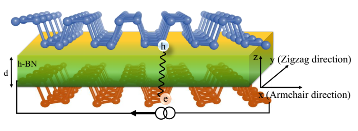
Motivated by the emergence of this experimentally accessible system, we investigate the CDW phase of carriers in coupled anisotropic electron-hole sheets where the electrons and holes interact via the Coulomb interaction. The anisotropy of the charge carriers is modeled by using anisotropic electron and hole masses. In this system, a negative electronic compressibility at sufficiently low density enables the formation of a CDW phase through the application of a uniform force field via the Coulomb drag. In the Coulomb drag setup shown in Fig. 1, applying the current in one of the layers, i.e. the “active” drive layer, induces an electric field in the other layer, i.e. the “passive” drag layer, in which no current flows. When the compressibility of the drag layer is negative, the force exerted by this electric field results in CDW phases with a wavelength determined by the absolute value of the compressibilityHroblak et al. (2017). We generalize the method of Ref. [Hroblak et al., 2017] to investigate the controlled formation of a CDW phase caused by a negative electronic compressibility. The CDW is normally understood to be an intrinsic instability of the electronic structure of the system. The electron liquid is generally protected against such instabilities by the same charge background but at low densities or at high magnetic fields a negative compressibility would be a sign of instability, leading to collapse or a phase transition such as the Wigner crystal Wigner (1934) or stripe phases Fogler (2002). In our proposed electron-hole (e-h) system, the negative compressibility of the layers produce CDW instability when an uniform drag force is applied to the layers. The approach
outlined in this paper is general and will be easily adaptable to other emerging anisotropic 2D materials. Our numerical analytics will be applied to phosphorene.
The paper is organized as follows. In Sec. II, we obtain the equilibrium solutions for the drag layer modeled as a quasi-1D system of a finite strip of length with density . We also calculate the anisotropic drag force applied to the drag layer that drives a CDW. We discuss the results of our work in Sec. III. Finally, we summarize our results in Sec. IV and discuss possible experimental observations and consequences.
II Theory
II.1 Charge density wave in double-layer phosphorene
We consider two strongly coupled electron and hole layers that are separated by an insulator. We assume that a uniform and steady force is applied to the carriers in each layer due to the momentum transfer processes in a drag set up configuration. We can characterize this force using an interlayer scattering time tensor , i.e. the rate at which momentum is transfered from the drive layer to the drag layer. Therefore, the force applied from the drive to the drag layer can be written as Gramila et al. (1991), where is the group velocity of carriers in the drive layer and is the mass tensor with diagonal elements and along (armchair) and (zigzag) directions, respectively. We solve the equilibrium solution for a single layer to which the drag force is applied. The drag layer is modeled as a quasi-1D electron(hole) gas on a finite strip of length with density . As no current can flow in the direction of the electric field, the drag force must be exactly balanced by the quantum mechanical force arising from the gradient of the chemical potential, . We note that is the chemical potential of the interacting system and is related to the ground state energy by , i.e. N is the number of particlesGiuliani and Vignale (2005); Luryi (1998). Assuming that the density remains uniform in the zigzag (armchair) direction, the equilibrium condition for the armchair () direction can be written as
| (1) |
where is the deviation of the 2D electron density from equilibrium with being the dielectric constant. In the linear regime, the gradient of the chemical potential is
| (2) |
Inserting both the drag and quantum mechanical forces in Eq. (1), we find the equilibrium condition for the direction
| (3) |
where is the scattering lifetime, the electric field is applied along the direction in the drive layer and the current is measured along the direction in the drag layer. We assume and express and in units of and divide the equilibrium solutions by the drag force. Therefore, the equilibrium condition for the direction of the layer becomes
| (4) |
where , and is a direction-dependent compressibility-related length given by
| (5) |
The density can be expanded in a series of Chebyshev polynomials
| (6) |
with the expansion coefficients. Using , where is associated with the second kind of Chebyshev polynomial, the derivative of the density is given by
| (7) |
Equations. (4)-(LABEL:eq:10) can be solved numerically for . By substituting these expressions into Eq. (4), multiplying both sides by , and integrating over with the help of standard integrals for the Chebyshev polynomials one can arrive at a set of linear algebraic equations for the coefficients ,
| (8) |
where is a matrix whose elements are given by
| (9) |
| (10) |
where is the inverse of the matrix . All equations apply to the zigzag () direction. In the next section, we obtain the interlayer scattering time.
II.2 Interlayer Scattering Rate
The Coulomb drag technique allows a unique access to the interlayer scattering rate via a resistance measurement. This can be simply shown within the Drude model Narozhny and Levchenko (2016). Considering an electron-hole double-layer system, the anisotropic drag resistivity is given by Saberi-Pouya et al. (2016)
| (11) | ||||
where the and indices refer to the and components. We assume that the drive layer contains electrons and the drag layer contains holes. Therefore, the drag resistivity depends on the interlayer momentum relaxation rate as
| (12) |
The dynamically screened interlayer potential can be obtained by solving the corresponding Dyson equation Badalyan and Peeters (2012),
| (13) |
where is the unscreened 2D Coulomb interaction, with being the interlayer separation. is the Coulomb potential and is the dynamic dielectric matrix of the system. Using the random phase approximation (RPA) formalism, we haveHwang and Das Sarma (2009); You and Wang (2012)
| (14) |
For an electron gas system, the noninteracting density–density response function can be obtained from the following equationBohm and Pines (1953):
| (15) |
Here is the Fermi-Dirac distribution, is the spin degeneracy, is the unit cell surface, and is the broadening parameter that may account for disorder in the system. Here, we extend our model to the case of e-h sheets where the energy bands are anisotropic. The corresponding Hamiltonian point can be expressed as Rodin et al. (2014)
| (16) |
where () is the energy of conduction (valence) band edge, and and describes the effective coupling between the conduction and valence bands. and are related to the anisotropic effective masses, which is our numerical analysis and will be taken like that of phosphoreneRodin et al. (2014),
| (17) | ||||
where is the energy band gap. Using Eq. (17), one can then use these masses to obtain an approximation for the spectrum Low et al. (2014); Liu et al. (2016),
| (18) |
where is the chemical potential of the electron(hole) layers. The temperature-dependent dynamical density-density response function for intra-band transitions can be calculated
| (19) | ||||
In the above symmetric form of temperature-dependent anisotropic density-density response function we have defined , , , with , is the 2D density of state mass, and
| (20) |
where and is the chemical potential of the electron and hole layers which is determined by the particle number conservation condition Ashcroft and Mermin (1976). We work in polar coordinates , in which the orientation factor is expressed as . At sufficiently low temperature and one can approximate by the low frequency expression
| (21) |
In this case, the screened potential of the electron-hole interaction in Eq. (13) can be approximated by the static interlayer Coulomb interaction in the long wave-length limit as
| (22) |
An important property of this equation is the compressibility, related to the small limit of the proper density-density response function of the compressibility sum rule Giuliani and Vignale (2005). There is an exact relation between the compressibility and the long wave-length limit of the static density-density response function as Giuliani and Vignale (2005). Inserting Eq. (22) in Eq. (11) we have
| (23) |
where is defined as
| (24) |
here is the screening wave vector related to compressibility. Since the most important contribution from the integration over comes from the region in which , we may neglect the first term in the denominator of Eq. (23) and obtain the simple form
| (25) |
| (26) |
This allows one to analytically obtain the integration over and , by using Gradshteyn and Ryzhik (2007). Since , the off diagonal elements of the drag resistivity vanish. The analytical results for the diagonal elements of the drag resistivity at low temperatures () becomes
| (27) |
One can then use this equation into Eq. (12) to get a diagonal tensor for the anisotropic interlayer scattering rate
| (28) |
For a system with equal electron and hole densities and equal chemical potentials, we have , where is the compressibility related length Hroblak et al. (2017).
III Results and discussion
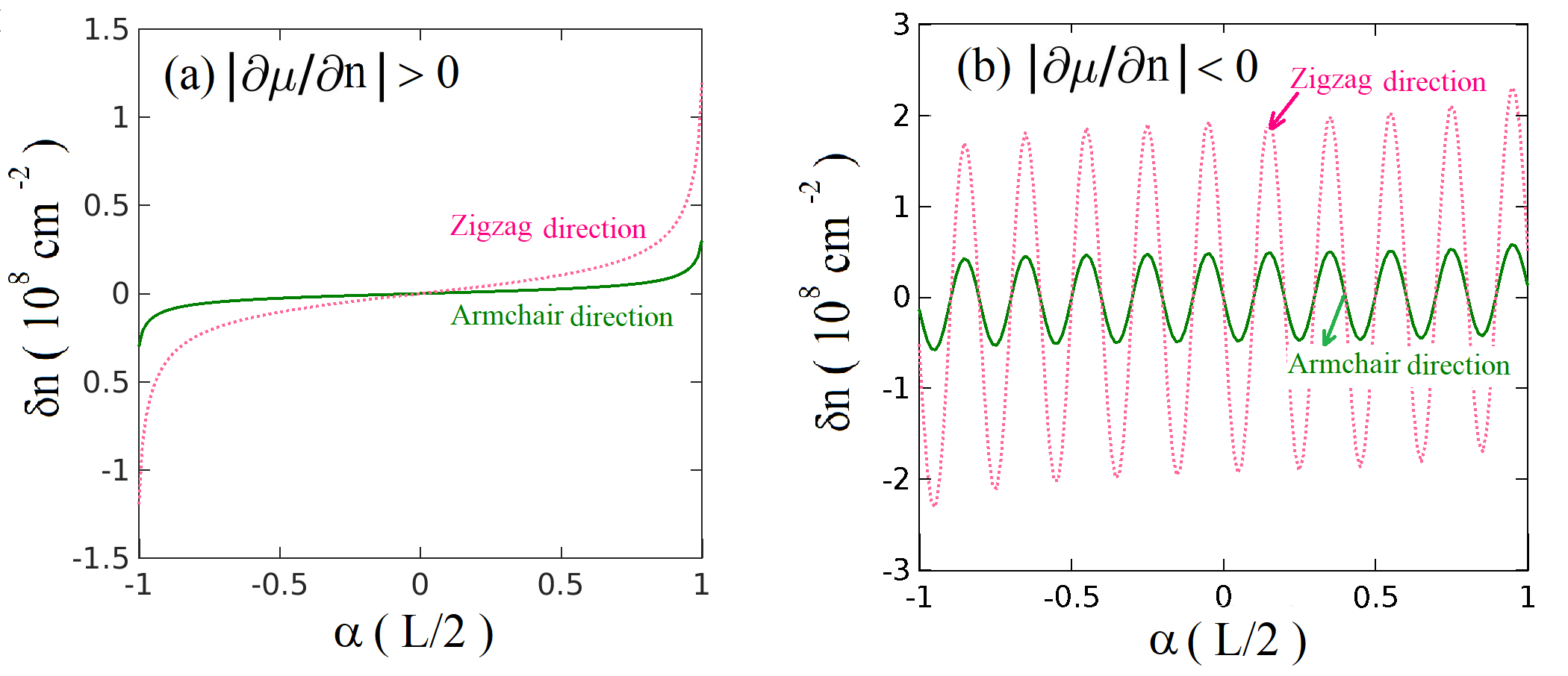
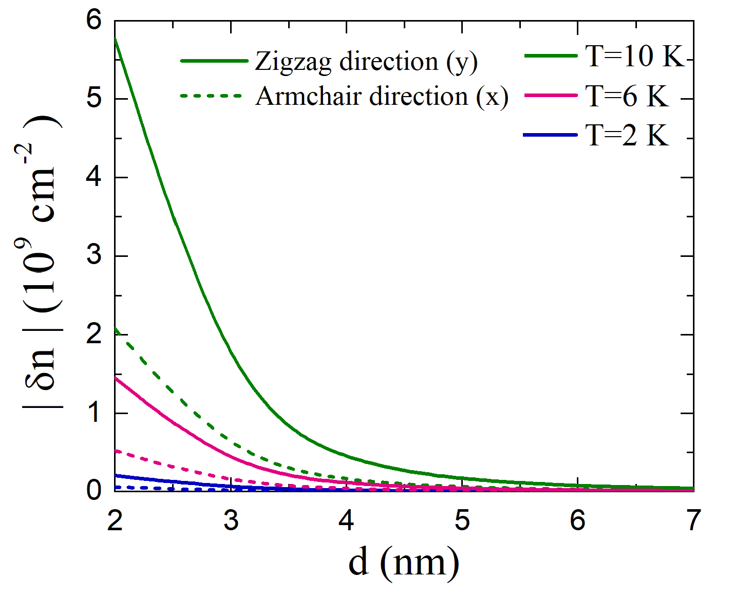
The density modulation depends directly on the system anisotropy and also on the sign of the compressibility. In order to explore the CDW in the phosphorene layer subjected to the drag force, we study the effects of the sign of the compressibility on the equilibrium solution, i.e. Eq. (4). In Fig. 2(a) we show the numerical results as calculated from the equilibrium solution for a positive compressibility ( ) in the armchair () and zigzag () directions of phosphorene with effective masses and and and with the velocity and Jin et al. (2016); Peng et al. (2014) with being the free electron mass. We set the dielectric constant Constantinescu and Hine (2016) for encapsulated phosphorene by h-BN layersHroblak et al. (2017) and L. We can see that similar to the case of an isotropic 2DEG Hroblak et al. (2017) the CDW is not stable for phosphorene along the directions where the compressibility is positive. Note that, the charge does not change at the center of phosphorene but it accumulates along the edges due to the strong electric field induced at the sharp edges. As a direct consequence of the band anisotropy the charge accumulation is different at the two directions of phosphorene. We show the charge modulation for phosphorene layers in Fig. 2(b) when the compressibility is negative. One can see that the density modulations along the zigzag () and armchair () directions have different amplitudes. The amplitude and frequency of these oscillations depend on the applied electric field and the value of in our Coulomb drag setup providing opportunity for electronic tuning. Moreover, phosphorene shows CDWs at higher densities as compared to typical 2D electron gas systems Hroblak et al. (2017). It is interesting to note that the periodicity of the CDW can be electrically tuned, via a gate, by the density of the drag layer, and hence the value of . As one can also see from Fig. 2(b), the wavelength of the CDW which is does not depend on the direction. The Coulomb interaction between the holes and electrons can also significantly enhance the occurrence of the CDW phase, especially when , where is the average distance between two neighboring in-plane carriers and , the effective Bohr radius. Figure. 3 shows the amplitude of the CDW along both zigzag and armchair directions as a function of the separation between the two layers at different temperatures. We find that the CDW state does become stable as the spacing between the layers is decreased. When we increase the separation , the density modulation decreases because at sufficiently large , the strength of the interlayer attraction is decreased. Moreover, as expected for Coulomb scattering in Fermi systems, the drag resistivity is approximately proportional to (see Eq. (27) in the manuscript and also Ref. [Seamons et al., 2009]). Therefore, higher temperatures result in larger drag and thus larger density modulation amplitudes. Also, it is predicted that the drag resistance will increase dramatically at the critical temperature below K where the paired electrons and holes want to move together to form an exciton condensate which is beyond our approach Seamons et al. (2009); Malliakas and Kanatzidis (2006). At very high temperatures, , the thermal fluctuations destroy any formation of a CDW phase. However, the results in Fig. 3 are at temperatures with (the equilibrium density corresponds to K) where carrier backscattering is neglected which will destroy the coherence Seamons et al. (2009); Hwang and Das Sarma (2008).
IV conclusion
In this paper, we considered a system of two strongly coupled electron-hole layers interacting by the Coulomb interaction. The system we proposed for phosphorene is expected to support large transresistivity Saberi-Pouya et al. (2016) due to the large effective mass of the carriers and consequently a large CDW modulation. Electrons and holes in the device are induced with top and bottom gates leading to controllable density in each layer. Separate electrical contacts to the two electron and hole layers allow the injection of current into one and the detection of a small drag voltage across the other. The drag voltage is a direct measure of the inter layer momentum relaxation rate. Measurements of this rate are in qualitative agreement with calculations of an interlayer Coulomb scattering model.
As we have mentioned, for an ordinary system the very same charge background that allows the compressibility to go negative is a major obstacle to the formation of charge-density waves due to the electrostatic energy cost that such waves would incur. However, in our manuscript and also in Ref. [Hroblak et al., 2017], it was shown that a uniform and steady force applied to the carriers when the compressibility is negative produces a charge-density wave. The force arising from the Coulomb drag effect is one way to apply such a steady force. Moreover, recent experiments on graphene-terminated BP heterostructures show an enhanced capacitance ),i.e., much larger than the expected geometric capacitance Wu et al. (2016). This enhanced capacitance results from a negative quantum capacitance when the compressibility ( ) becomes negative. We have shown that a negative compressibility at low carrier concentrations by using the external force that arises from the Coulomb drag effect is one way to produce the density modulation in the drag layer. We obtained the equilibrium solutions for the drag layer modeled as a quasi-1D system. By using the compressibility sum rule in which the compressibility is related to the small momentum limit of the proper density-density response function, an analytical expression was obtained for the anisotropic drag force. We found that the density modulation not only depends on the sign of the compressibility but also depends on the system anisotropy. The amplitude of the CDW phase depends on the separation between the layers and temperature. The wave-length of the CDW can be also electrically tuned by changing the value of . This might be changed in experiment , via a gate, changing the density of the passive layer.
There are a number of ways that a CDW phase could be experimentally identified DiMasi et al. (1995). This phase can be detected by optical methods, such as differential absorption or diffraction and also by using STM, which can detect a number of features related to the onset of CDW, including charge modulation, periodic distortion of atomic position, and the opening of a gap in the density of states. Angle resolved photoemission spectroscopy (ARPES) can also show which portions of the Fermi surface are gapped out by the CDW Fang et al. (2007). This can give guidance as to whether the CDW is driven by Fermi surface nesting or by something more exotic Perfetti et al. (2008). By perturbing
a material with an ultrashort laser pulse and following the resulting transient ARPES spectra, one can obtain insight into the dynamics both of quasiparticle occupations and of the electronic structure itself Smallwood et al. (2016). To evaluate the feasibility of optical detection of such an anisotropic CDW in BP, we note that the angular dependence of the differential reflection signal can be induced by both the pump absorption and the probe detection efficiency He et al. (2015). It was shown that by rotating the sample with respect to the pump polarization, the pump injects different carrier densities and the anisotropic band structure causes the probe pulses with different polarizations to sense the carriers with different efficiencies He et al. (2015). The CDW phase could also be identified using STM. Due to the formation of the CDW along with the associated periodic lattice distortion, a gap in the Fermi surface opens. This modifies the local density of states which could be detected by tunneling Grüner (1988); Slough et al. (1988); Coleman et al. (1988); Brun et al. (2010). A CDW phase can be also detected by transport measurements. 1D stripes may be pinned by disorder, in which case the CDW could be identified either with standard threshold voltage conductivity measurements or with frequency threshold measurements of ac conductivity Hall and Zettl (1988). Our approach is general and applicable to other 2D materials with anisotropic parabolic energy bands.
Acknowledgements
This work was partially supported by the Flemish Science Foundation (FWO-Vl) and the Methusalem program of the Flemish government and Iran Science Elites Federation.
References
- Hroblak et al. (2017) E. E. Hroblak, A. Principi, H. Zhao, and G. Vignale, Phys. Rev. B 96, 075422 (2017).
- Prishchenko et al. (2017) D. A. Prishchenko, V. G. Mazurenko, M. I. Katsnelson, and A. N. Rudenko, 2D Materials 4, 025064 (2017).
- Aierken et al. (2015) Y. Aierken, D. Çak ır, C. Sevik, and F. M. Peeters, Phys. Rev. B 92, 081408 (2015).
- Saberi-Pouya et al. (2016) S. Saberi-Pouya, T. Vazifehshenas, M. Farmanbar, and T. Salavati-fard, J. Phys. Condens. Matter 28, 285301 (2016).
- Zhu et al. (2016) W. Zhu, S. Park, M. N. Yogeesh, K. M. McNicholas, S. R. Bank, and D. Akinwande, Nano Lett. 16, 2301 (2016).
- Doh and Choi (2017) H. Doh and H. J. Choi, 2D Materials 4, 025071 (2017).
- Saberi-Pouya et al. (2017a) S. Saberi-Pouya, T. Vazifehshenas, T. Salavati-fard, M. Farmanbar, and F. M. Peeters, Phys. Rev. B 96, 075411 (2017a).
- Rodin et al. (2014) A. S. Rodin, A. Carvalho, and A. H. Castro Neto, Phys. Rev. Lett. 112, 176801 (2014).
- Çakır et al. (2014) D. Çakır, H. Sahin, and F. M. Peeters, Phys. Rev. B 90, 205421 (2014).
- Carvalho et al. (2016) A. Carvalho, M. Wang, X. Zhu, A. S. Rodin, H. Su, and A. H. C. Neto, Nat. Rev. Mater. 1, 16061 (2016).
- Saberi-Pouya et al. (2018) S. Saberi-Pouya, M. Zarenia, A. Perali, T. Vazifehshenas, and F. M. Peeters, Phys. Rev. B 97, 174503 (2018).
- Ge et al. (2015) S. Ge, C. Li, Z. Zhang, C. Zhang, Y. Zhang, J. Qiu, Q. Wang, J. Liu, S. Jia, J. Feng, and D. Sun, Nano Lett. 15, 4650 (2015).
- Wang et al. (2015) X. Wang, A. M. Jones, K. L. Seyler, V. Tran, Y. Jia, H. Zhao, H. Wang, L. Yang, X. Xu, and F. Xia, Nat. Nanotechnol. 10, 517 (2015).
- Brent et al. (2014) J. R. Brent, N. Savjani, E. A. Lewis, S. J. Haigh, D. J. Lewis, and P. O’Brien, Chem. Commun. 50, 13338 (2014).
- Shao et al. (2016) L. Shao, H. Ye, Y. Wu, D. Yinxiao, P. Ding, F. Zeng, and Q. Yuan, Materials Research Express 3, 025013 (2016).
- Saberi-Pouya et al. (2017b) S. Saberi-Pouya, T. Vazifehshenas, T. Salavati-fard, and M. Farmanbar, Phys. Rev. B 96, 115402 (2017b).
- Bokdam et al. (2011) M. Bokdam, P. A. Khomyakov, G. Brocks, Z. Zhong, and P. J. Kelly, Nano Lett. 11, 4631 (2011).
- Wu et al. (2016) Y. Wu, X. Chen, Z. Wu, S. Xu, T. Han, J. Lin, B. Skinner, Y. Cai, Y. He, C. Cheng, and N. Wang, Phys. Rev. B 93, 035455 (2016).
- Tőke and Fal’ko (2014) C. Tőke and V. I. Fal’ko, Phys. Rev. B 90, 035404 (2014).
- Eisenstein et al. (1994) J. P. Eisenstein, L. N. Pfeiffer, and K. W. West, Phys. Rev. B 50, 1760 (1994).
- Li et al. (2011) L. Li, C. Richter, S. Paetel, T. Kopp, J. Mannhart, and R. C. Ashoori, Science 332, 825 (2011).
- Grüner (1988) G. Grüner, Rev. Mod. Phys. 60, 1129 (1988).
- Slough et al. (1988) C. G. Slough, B. Giambattista, A. Johnson, W. W. McNairy, C. Wang, and R. V. Coleman, Phys. Rev. B 37, 6571 (1988).
- Coleman et al. (1988) R. Coleman, B. Giambattista, P. Hansma, A. Johnson, W. McNairy, and C. Slough, Advances in Physics 37, 559 (1988).
- Brun et al. (2010) C. Brun, Z.-Z. Wang, P. Monceau, and S. Brazovskii, Phys. Rev. Lett. 104, 256403 (2010).
- Zarenia et al. (2017) M. Zarenia, D. Neilson, and F. M. Peeters, Sci. Rep. 7, 11510 (2017).
- Zarenia et al. (2014) M. Zarenia, A. Perali, D. Neilson, and F. Peeters, Sci. Rep. 4, 7319 (2014).
- Kotov et al. (2012) V. N. Kotov, B. Uchoa, V. M. Pereira, F. Guinea, and A. H. Castro Neto, Rev. Mod. Phys. 84, 1067 (2012).
- Wigner (1934) E. Wigner, Phys. Rev. 46, 1002 (1934).
- Fogler (2002) M. M. Fogler, High Magnetic Fields: Applications in Condensed Matter and Spectroscopy (Springer,Berlin, 2002).
- Gramila et al. (1991) T. J. Gramila, J. P. Eisenstein, A. H. MacDonald, L. N. Pfeiffer, and K. W. West, Phys. Rev. Lett. 66, 1216 (1991).
- Giuliani and Vignale (2005) G. Giuliani and G. Vignale, Quantum theory of the electron liquid (Cambridge University Press, 2005).
- Luryi (1998) S. Luryi, Appl. Phys. Lett. 52, 501 (1998).
- Narozhny and Levchenko (2016) B. N. Narozhny and A. Levchenko, Rev. Mod. Phys. 88, 025003 (2016).
- Badalyan and Peeters (2012) S. M. Badalyan and F. M. Peeters, Phys. Rev. B 86, 121405 (2012).
- Hwang and Das Sarma (2009) E. H. Hwang and S. Das Sarma, Phys. Rev. B 80, 205405 (2009).
- You and Wang (2012) W.-L. You and X.-F. Wang, Nanotechnology 23, 505204 (2012).
- Bohm and Pines (1953) D. Bohm and D. Pines, Phys. Rev. 92, 609 (1953).
- Low et al. (2014) T. Low, R. Roldán, H. Wang, F. Xia, P. Avouris, L. M. Moreno, and F. Guinea, Phys. Rev. Lett. 113, 106802 (2014).
- Liu et al. (2016) Y. Liu, T. Low, and P. P. Ruden, Phys. Rev. B 93, 165402 (2016).
- Ashcroft and Mermin (1976) N. Ashcroft and N. Mermin, Solid State Physics (Saunders College, Philadelphia, 1976).
- Gradshteyn and Ryzhik (2007) I. Gradshteyn and I. Ryzhik, Table of Integrals, Series, and Products (Academic Press, 2007).
- Jin et al. (2016) Z. Jin, J. T. Mullen, and K. W. Kim, Appl. Phys. Lett. 109, 053108 (2016).
- Peng et al. (2014) X. Peng, Q. Wei, and A. Copple, Phys. Rev. B 90, 085402 (2014).
- Constantinescu and Hine (2016) G. C. Constantinescu and N. D. M. Hine, Nano Lett. 16, 2586 (2016).
- Seamons et al. (2009) J. A. Seamons, C. P. Morath, J. L. Reno, and M. P. Lilly, Phys. Rev. Lett. 102, 026804 (2009).
- Malliakas and Kanatzidis (2006) C. D. Malliakas and M. G. Kanatzidis, Journal of the American Chemical Society 128, 12612 (2006).
- Hwang and Das Sarma (2008) E. H. Hwang and S. Das Sarma, Phys. Rev. B 78, 075430 (2008).
- DiMasi et al. (1995) E. DiMasi, M. C. Aronson, J. F. Mansfield, B. Foran, and S. Lee, Phys. Rev. B 52, 14516 (1995).
- Fang et al. (2007) A. Fang, N. Ru, I. R. Fisher, and A. Kapitulnik, Phys. Rev. Lett. 99, 046401 (2007).
- Perfetti et al. (2008) L. Perfetti, P. A. Loukakos, M. Lisowski, U. Bovensiepen, M. Wolf, H. Berger, S. Biermann, and A. Georges, New J. Phys. 10, 053019 (2008).
- Smallwood et al. (2016) C. L. Smallwood, R. A. Kaindl, and A. Lanzara, EPL 115, 27001 (2016).
- He et al. (2015) J. He, D. He, Y. Wang, Q. Cui, M. Z. Bellus, H.-Y. Chiu, and H. Zhao, Nano Lett. 9, 6436 (2015).
- Hall and Zettl (1988) R. P. Hall and A. Zettl, Phys. Rev. B 38, 13019 (1988).