Superconductivity Induced at a Point Contact on the Topological Semimetal Tungsten Carbide
Abstract
We report the observation of local superconductivity induced at the point contact formed between a normal metal tip and WC – a triple point topological semimetal with super hardness. Remarkably, the maximum critical temperature is up to near 12 K but insensitive to the tip’s magnetism. The lateral dimensions of the superconducting puddles were evaluated and the temperature dependencies of superconducting gap and upper critical field were also obtained. These results put constraints on the explanation of the induced superconductivity and pave a pathway for exploring topological superconductivity.
Unconventional superconductors and topological materials have attracted tremendous attentions due to their novel physical properties and potential applications. Integration of superconductivity and topological nature may lead to new emergent phenomena such as exotic topological superconductivity, for the interesting interplay between electron pairing and the spin-orbit coupling Qi and Zhang (2011); Leijnse and Flensberg (2012); Alicea (2012); Sato and Ando (2017). Recently, superconductivity was induced at a point contact between a normal metal tip and the 3D Dirac semimetal Cd3As2 Aggarwal et al. (2015); Wang et al. (2015). Soon after, similar phenomenon was reproduced in the Weyl semimetal TaAs Aggarwal et al. (2017); Wang et al. (2017). In particular, the induced superconductivity could coexist with preserved topological properties in the line-nodal semimetal ZrSiS Aggarwal et al. (2019). Such tip-induced superconductivity (TISC) is very exciting since it is extremely rare in common metals and provides a unique way of searching topological superconductivity Wang et al. (2018). Although the most likely origins of the TISC were speculated to be tip pressure-induced band reconstruction, confinement effect, charge carrier doping Aggarwal et al. (2017), or remarkable enhancement of density of states under the tip Aggarwal et al. (2019), the dominant mechanism remains elusive. Meanwhile, unconventional superconductivity has been proposed for Cd3As2, yet based on two distinct experimental observations, i.e., a pseudogap behavior above the critical temperature Aggarwal et al. (2015) or an abnormal spectral shape at low temperatures Wang et al. (2015). For TaAs, such unconventionality is still in debate Aggarwal et al. (2017); Wang et al. (2017). Therefore, more evidences are desired to clarify this issue.
Most recently, a new type of topological quasiparticles was proposed for the metals hosting symmetry-protected three-band crossings (three-fold degeneracy) near the Fermi level Zhu et al. (2016); Weng et al. (2016a, b). These triple point fermions were first observed in MoP Lv et al. (2017) and the non-trivial topology of the new semimetal state was identified in WC subsequently Ma et al. (2018). As a triple point topological semimetal, WC can be regarded as an intermediate state between Dirac and Weyl semimetals with four- and two-fold degenerate points, respectively. Furthermore, the super hardness of WC ensures its topological band structure to be robust against tip pressure, providing an ideal platform to inspect the universality and mechanism of TISC in topological semimetals.
In this work, we performed point contact experiments on WC using both non-magnetic and ferromagnetic normal metal tips. Local superconductivity with various lateral sizes could be induced for all these tips, providing a strong evidence of its unconventional nature. In addition, temperature dependent superconducting gap and upper critical field were obtained. These observations are helpful to reveal the mechanism of TISC in topological semimetals and deserve to be studied intensively.
Point contact measurements were carried out in our home-built probes based on a physical property measurement system (PPMS) from Quantum Design. We adopted here the most common point contact (PC) configuration, often called “needle-anvil” as illustrated in Fig. 2(a). An ultrafine differential micrometer (Siskiyou 100tpi-05d) or an Attocube nanopositioner stack was used to control tip approaching towards a sample along the longitudinal axis of PPMS, and a pair of bevel gears was used for tip approaching horizontally. Point contacts (PCs) between various metal tips and three crystalline WC specimens (labeled as WC01, WC02 and WC03) were formed in situ with current injecting along the [001]-axis of WC crystals. During the spectral measurements, current-voltage () curves and differential conductance spectra () were recorded simultaneously.
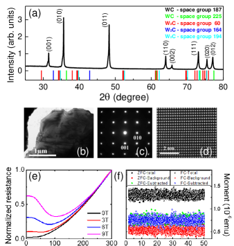
The high-quality single crystals of WC studied here were grown by the flux method He et al. (2017), with a dimension around 2 mm2 and a thicknesses from 0.3 mm to 0.65 mm. The high purity of the WC samples has been confirmed by XRD and TEM measurements. Fig.1(a) shows the room-temperature powder XRD pattern of WC obtained by grinding lots of single crystals synthesized in this work. All the diffraction peaks can be well indexed by the hexagonal structure of WC with a space group of (No.187). We didn’t find any peaks indexed by the other structures of WC or W2C with space groups shown in Fig.1(a) Matthias and Hulm (1952); Willens and Buehler (1965); Willens et al. (1967). Figures 1(b) - (d) shows the typical bright field TEM image, electron diffraction pattern and the corresponding HAADF STEM image taken along the [100] zone axis direction. The repeated TEM measurements reveal no signatures of any impurity phase rather than the expected hexagonal WC. As shown in Fig. 1(e), the temperature dependent resistance curves in various magnetic fields show large magnetoresistance at low temperature, consistent with the previous measurementHe et al. (2017), whereas no superconducting transition has been detected down to the lowest temperature of 2 K. Figure 1(f) displays the raw data of magnetization versus temperature, in which both total signal and background signal for empty holder are provided. Obtained by subtracting background signals from total signals, the nominal sample signals are of the order of 10-7 emu, around the minimal detectivity of the Quantum Design MPMS system. In the narrow temperature range studied here, the nominal sample signals are temperature independent, indicating again no superconductivity existing in the sample.
In general, curves of a PC between two normal metals (N/N) look more like straight lines at low bias voltages due to its nearly constant resistance, and no obvious features can be seen in the PC spectra . The situation is very different for a normal metal/superconductor (N/S) PC. When superconducting state is turned on, the spectral shape will depend on the superconducting pairing symmetry and the effective barrier height at the N/S interface, which could be described by a generalized Blonder-Tinkham-Klapwijk (BTK) formalism Blonder et al. (1982); Dynes et al. (1984); Pleceník et al. (1994); Tanaka and Kashiwaya (1995); Deutscher (2005). A PC spectrum with lower barrier height is usually referred to as Andreev reflection spectrum (the bottom line in Fig. 2(b)). Since Andreev reflection roots in the formation of Cooper pairs in a superconductor, it is a unique and convincing evidence of superconductivityDaghero and Gonnelli (2010); Daghero et al. (2011). Although the p-wave spectrum with current injection along nodal direction is similar to the curve of s-wave (the middle line in Fig. 2(b)), the anti-nodal spectrum shows a significant zero-bias conductance peak (ZBCP) due to the formation of Andreev bound states (the top line in Fig.2(b)), which have usually been utilized to identify unconventional superconductivityDaghero and Gonnelli (2010); Deutscher (2005). However, it should be pointed out that, the above-mentioned cases are based on the ideal ballistic limit, i.e., the contact radius is much smaller than the electron mean free path (). If , i.e., the thermal regime is dominant, a non-intrinsic ZBCP could often be observed for both nodeless and nodal superconductors. In this regime, the inelastic scattering of electrons in the contact region will cause Joule heating and a local rise in temperature with increasing current Jansen et al. (1980); Duif et al. (1989); Daghero and Gonnelli (2010). A superconducting to normal transition will occur at a specific current and a spurious ZBCP arises in the PC spectrum, which is called “critical current effect” Westbrook and Javan (1999); Shan et al. (2003); Sheet et al. (2004); Gifford et al. (2016), as illustrated in Fig. 2(c). From this perspective, a measured ZBCP cannot be a conclusive evidence of unconventional superconductivity.
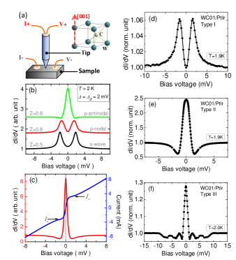
Though the as-grown WC single crystal is not superconductive, it was found that superconductivity could be induced at the point contact formed between a normal metal tip and WC with a good repeatability involving all the used tips and the studied samples. As demonstrated in Figs. 2(d)-(f), the obtained spectra can be classified into three categories: (I) with a typical Andreev reflection spectral shape, (II) showing a zero-bias conductance peak (ZBCP) and two symmetric dips beside it, and (III) having a ZBCP with multiple pairs of dips. As above-mentioned, unconventional pairing symmetries could give a ZBCP by generating zero-energy bound states at N/S interface Deutscher (2005), or alternatively, topological superconductors could contribute significant zero-energy density of states at boundaries or impurities due to their nontrivial topology Qi and Zhang (2011); Leijnse and Flensberg (2012); Alicea (2012); Sato and Ando (2017). For the latter two cases, the symmetric dips beside the ZBCP locate near the superconducting gap energy Tanaka and Kashiwaya (1995); Yamakage et al. (2012), thus don’t depend on the junction resistance if only the gap is unchangeable. We find that some of the experimental data coincide with this expectation, but some other results exhibit mutable dip energy by changing junction resistance. Although an additional resistance inherent in pseudo-four-probe electrical measurements could lead to a spurious uncertainty of the characteristic energies Chen et al. (2010), we believe that critical current effect should be involved in, at least, some of our measurements. Based on these knowledge, it could be deduced that the spectra of type III are contributed by multiple parallel channels, corresponding to different micro-constrictions in the large contact area Bugoslavsky et al. (2004); Miyoshi et al. (2005); Shan et al. (2006). This mechanism can be further verified by the data in Figure 5.
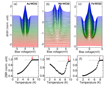
Figures 3(a)-(c) show temperature dependent spectra for three PCs prepared with the non-magnetic Au and PtIr tips and a ferromagnetic Fe tip, respectively. Both the Andreev reflection and ZBCP signals vanish at the corresponding superconducting critical temperature, therefore can be determined by the onset of the resistive transition. In order to highlight superconducting transition and determine , the zero-bias resistance (ZBR) derived from Figs. 3(a)-(c) is plotted against temperature in Figs. 3(d)-(f). It can be seen that for multiple-channel PCs, more than one transitions might be observed. All values obtained in this work are summarized in Fig. 4, with the maximum value close to 12 K and the minimum one about 4 K. The wide distribution of critical temperatures especially for the different channels of a specified PC indicates that the induced superconductivity is quite local and depends on the real condition of each microcontact in the contact area. Such local superconductivity is difficult to be detected by macroscopic measurements of resistance and magnetization, hence additional techniques other than point contact are necessary to rebuild it in a larger scale. As a preliminary attempt, we have made some progress in metal film deposition on WC crystals Zhu et al. (2018). However, a connected superconducting area large enough is yet to be achieved.
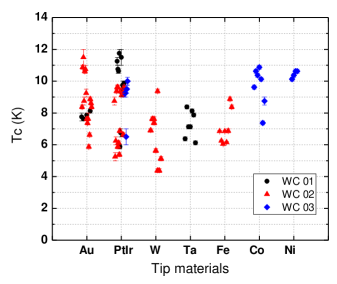
Another interesting finding here is that local superconductivity can be triggered on non-superconducting WC by ferromagnetic Fe, Co and Ni tips as well as the nonmagnetic tips made of PtIr alloy, Au, W, and Ta, providing a strong evidence for its unconventional nature. The measured signals are significant with a good repeatability, ruling out experimental occasionality. Remarkably, the maximal achieved by a particular metal tip is not sensitive (almost irrelevant) to the tips’ magnetism. This is surprising because it is well known that ferromagnetism will break spin singlet pairing and suppress conventional superconductivity, especially for a thin film similar to the interfacial superconductivity observed here. According to the previous works on conventional superconductor-ferromagnet heterostructures, a ferromagnetic layer could seriously suppress or even kill the superconductivity of superconducting layers depending on their thickness Bourgeois and Dynes (2002); Sidorenko et al. (2003); Gong et al. (2015). Another different case is a contact between a ferromagnet and a bulk superconductor, where the bulk superconductivity can be preserved and thus can be used to measure the spin polarization of the adjacent ferromagnet Ji et al. (2002). However, those experiments are all quite different from our situation, in which interfacial superconductivity could be induced by the ferromagnetic tips even with similar s as the non-magnetic tips. The compatibility of induced superconductivity and ferromagnetism suggests an unconventional pairing component Fay and Appel (1980); Cho et al. (2012); Wei et al. (2014), which deserves further experimental and theoretical investigations.
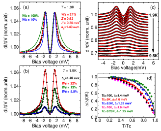
In order to get further insight into the observed TISC, the measured Andreev-reflection spectra were studied in detail as exemplified in Fig. 5(a). A revised two-channel BTK model was adopted Blonder et al. (1982); Dynes et al. (1984); Pleceník et al. (1994); Tanaka and Kashiwaya (1995) to take into account the contribution from both superconducting and normal channels, in which the parameters of , , and are superconducting gap, effective barrier height, broadening factor and the spectral weight contributed by the superconducting channel. Thus the total conductance can be written as (having been normalized according to the normal conductance ). It was found that, the simulation with an appropriate can fit the data of Fig. 5(a) very well, whereas neither a single channel () or an underestimated value of (say, ) cannot. Moreover, as shown in Fig. 5(b), a slight adjustment of junction resistance could lead to a change of without altering the nature of the superconducting channel. These analyses indicate the validity of the multiple-channel model and the finite size of the superconducting area beneath the tip. Combining the resistance of a superconducting channel () and its effective barrier , we can evaluate the lateral dimension () of the superconducting channel using the well-known expression of Sharvin resistance for a micro-constriction in the ballistic limit, i.e., Blonder et al. (1982), where is the bulk resistivity of the two banks of a PC. As a rough estimate, is taken as cm by considering cm He et al. (2017) and cm Matula (1979), and the mean free path can be approximated using the above resistivity Orlando et al. (1979) to be m and m for WC and Au, respectively. From the fitting in Fig. 5(a), can be determined by with the total junction resistance of . All the parameters lead to a lateral dimension of the superconducting channel as low as 10 nm. Considering that the contact size in thermal regime is much larger than the mean free path, we could give a conservative estimation that the induced local superconductivity could have a dimension varying from tens of nanometers to the order of micrometer. On the one hand, the magnetic compatible superconductivity achieved at nano-scale apparently contradicts the conventional Bardeen-Cooper-Schrieffer (BCS) theory with spin-singlet pairing Bourgeois and Dynes (2002); Sidorenko et al. (2003); Gong et al. (2015). On the other hand, the superconducting region realized in micron degree will make it possible to be extended to a much larger scale by using appropriate ways such as metal film deposition. Figure 5(c) demonstrates the global fitting of a series of temperature dependent spectra. The superconducting gaps obtained from all such fittings are summarized in Fig. 5(d). The temperature dependencies of the superconducting gaps do not merge into each other but distribute randomly around the BCS law, which could be a consequence of multi-band superconductivity Daghero and Gonnelli (2010) or the unconventional property of the TISC.
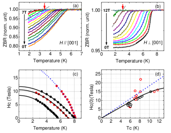
The TISC on WC in addition to Cd3As2 Aggarwal et al. (2015); Wang et al. (2015) and TaAs Aggarwal et al. (2017); Wang et al. (2017) implies a common mechanism shared by these topological semimetals. Among several possible explanations, the first candidate is band structure modifications induced by tip pressure as proposed in previous studies. However, this speculation is inconsistent with our finding that a soft Au tip could induce a of 11.5 K on WC, even higher than that of 7.5 K achieved by a W tip. In fact, WC has a hardness of near 2000 kg/mm2 (along c-axis) at room temperature, which is much higher than that of Au (100-200 kg/mm2). Moreover, no superconductivity above 1.5 K can be observed in our WC samples under a very high hydrostatic pressure up to 11 GPa. Therefore, tip pressure effect can be ruled out in our experiments. Meanwhile, as aforementioned, the lateral size of the superconducting puddles can be as large as the order of micrometer, implying the confinement effect is also irrelevant here. So, the TISC observed here is closely related to the interface coupling between normal metals and WC. In this case, a two dimensional superconductivity might be involved Saito et al. (2016). To examine the expected 2D scenario, we have measured critical magnetic field for different configurations of and (henceforth referred to as and ). As exemplified by Figs. 6(a)-(c), the determined relations obviously deviate from the 2D regime dictating and . It was found that all s and most s can be approximated by the empirical formula of . Whereas in some cases, can be described by a trial formula of which lies between the empirical square law and the 2D square root law. This suggests that the induced superconductivity locates at the boundary of the 3D and 2D regimes, which might be ascribed to a superconducting layer with a significant thickness. All determined by extrapolating to zero temperature are plotted against in Fig. 6(d). Although most data follow a common trend indicated by the black solid line, some points of have much larger values exceeding Pauli paramagnetic limit.
In summary, we have observed TISC up to near 12 K on the newfound topological semimetal WC with super hardness. The estimated lateral dimensions of the superconducting regions vary from dozens of nanometers to the order of micrometer, and the determined temperature dependencies of superconducting gap and critical field behave differently from the conventional superconductivity. Most surprisingly, the achieved critical temperature is insensitive to the ferromagnetism of the tip materials. These findings not only reveal the unconventional nature of the TISC but also support interface coupling instead of tip-pressure or confinement effect as the dominant origin. Furthermore, the high chemical stability and super hardness of WC offer an opportunity to fabricate metal/WC interface and explore exotic quantum phenomena in this topological material.
Acknowledgements.
This work was financially supported by the National Key R&D Program of China (2017YFA0302904, 2018YFA0305602, 2016YFA0300604, 2015CB921303, 2018YFA0305700, 2017YFA0303201), the National Natural Science Foundation of China (11574372, 11322432, 11404175, 11874417, 11804379, 11674331), the National Basic Research Program of China 973 Program (Grant No.2015CB921303), the “Strategic Priority Research Program (B)” of the Chinese Academy of Sciences ( Grant No. XDB07020300, XDB07020100), the 100 Talents Project of the Chinese Academy of Sciences; CASHIPS Director’s Fund (No. BJPY2019B03) and The Recruitment Program for Leading Talent Team of Anhui Province (2019-16).References
- Qi and Zhang (2011) X.-L. Qi and S.-C. Zhang, Rev. Mod. Phys. 83, 1057 (2011), URL https://link.aps.org/doi/10.1103/RevModPhys.83.1057.
- Leijnse and Flensberg (2012) M. Leijnse and K. Flensberg, Semicond. Sci. Technol. 27, 124003 (2012), ISSN 0268-1242, URL http://dx.doi.org/10.1088/0268-1242/27/12/124003.
- Alicea (2012) J. Alicea, Rep. Prog. Phys. 75, 076501 (2012), ISSN 0034-4885, URL http://dx.doi.org/10.1088/0034-4885/75/7/076501.
- Sato and Ando (2017) M. Sato and Y. Ando, Rep. Prog. Phys. 80, 076501 (2017), ISSN 0034-4885, URL http://dx.doi.org/10.1088/1361-6633/aa6ac7.
- Aggarwal et al. (2015) L. Aggarwal, A. Gaurav, Z. Thakur, Gohil S.and Haque, A. K. Ganguli, and G. Sheet, Nature Materials 15, 32 (2015), URL https://doi.org/10.1038/nmat4455.
- Wang et al. (2015) H. Wang, H. Wang, H. Liu, H. Lu, W. Yang, S. Jia, X.-J. Liu, X. C. Xie, J. Wei, and J. Wang, Nature Materials 15, 38 (2015), URL https://doi.org/10.1038/nmat4456.
- Aggarwal et al. (2017) L. Aggarwal, S. Gayen, S. Das, R. Kumar, V. Süß, C. Felser, C. Shekhar, and G. Sheet, Nature Communications 8, 13974 (2017), article, URL https://doi.org/10.1038/ncomms13974.
- Wang et al. (2017) H. Wang, H. Wang, Y. Chen, J. Luo, Z. Yuan, J. Liu, Y. Wang, S. Jia, X.-J. Liu, J. Wei, et al., Science Bulletin 62, 425 (2017), ISSN 2095-9273, URL http://www.sciencedirect.com/science/article/pii/S2095927317301007.
- Aggarwal et al. (2019) L. Aggarwal, C. K. Singh, M. Aslam, R. Singha, A. Pariari, S. Gayen, M. Kabir, P. Mandal, and G. Sheet, 31, 485707 (2019), ISSN 0953-8984, URL http://dx.doi.org/10.1088/1361-648X/ab3b61.
- Wang et al. (2018) H. Wang, L. Ma, and J. Wang, Science Bulletin 63, 1141 (2018), ISSN 2095-9273, URL http://www.sciencedirect.com/science/article/pii/S2095927318303712.
- Zhu et al. (2016) Z. Zhu, G. W. Winkler, Q. Wu, J. Li, and A. A. Soluyanov, Phys. Rev. X 6, 031003 (2016), URL https://link.aps.org/doi/10.1103/PhysRevX.6.031003.
- Weng et al. (2016a) H. Weng, C. Fang, Z. Fang, and X. Dai, Phys. Rev. B 93, 241202 (2016a), URL https://link.aps.org/doi/10.1103/PhysRevB.93.241202.
- Weng et al. (2016b) H. Weng, C. Fang, Z. Fang, and X. Dai, Phys. Rev. B 94, 165201 (2016b), URL https://link.aps.org/doi/10.1103/PhysRevB.94.165201.
- Lv et al. (2017) B. Q. Lv, Z.-L. Feng, Q.-N. Xu, X. Gao, J.-Z. Ma, L.-Y. Kong, P. Richard, Y.-B. Huang, V. N. Strocov, C. Fang, et al., Nature 546, 627 (2017), URL https://doi.org/10.1038/nature22390.
- Ma et al. (2018) J.-Z. Ma, J.-B. He, Y.-F. Xu, B. Q. Lv, D. Chen, W.-L. Zhu, S. Zhang, L.-Y. Kong, X. Gao, L.-Y. Rong, et al., Nature Physics 14, 349 (2018), ISSN 1745-2481, URL https://doi.org/10.1038/s41567-017-0021-8.
- He et al. (2017) J. B. He, D. Chen, W. L. Zhu, S. Zhang, L. X. Zhao, Z. A. Ren, and G. F. Chen, Phys. Rev. B 95, 195165 (2017), URL https://link.aps.org/doi/10.1103/PhysRevB.95.195165.
- Matthias and Hulm (1952) B. T. Matthias and J. K. Hulm, Phys. Rev. 87, 799 (1952), URL https://link.aps.org/doi/10.1103/PhysRev.87.799.
- Willens and Buehler (1965) R. H. Willens and E. Buehler, Applied Physics Letters 7, 25 (1965), eprint https://doi.org/10.1063/1.1754239, URL https://doi.org/10.1063/1.1754239.
- Willens et al. (1967) R. H. Willens, E. Buehler, and B. T. Matthias, Phys. Rev. 159, 327 (1967), URL https://link.aps.org/doi/10.1103/PhysRev.159.327.
- Blonder et al. (1982) G. E. Blonder, M. Tinkham, and T. M. Klapwijk, Phys. Rev. B 25, 4515 (1982), URL https://link.aps.org/doi/10.1103/PhysRevB.25.4515.
- Dynes et al. (1984) R. C. Dynes, J. P. Garno, G. B. Hertel, and T. P. Orlando, Phys. Rev. Lett. 53, 2437 (1984), URL https://link.aps.org/doi/10.1103/PhysRevLett.53.2437.
- Pleceník et al. (1994) A. Pleceník, M. Grajcar, i. c. v. Beňačka, P. Seidel, and A. Pfuch, Phys. Rev. B 49, 10016 (1994), URL https://link.aps.org/doi/10.1103/PhysRevB.49.10016.
- Tanaka and Kashiwaya (1995) Y. Tanaka and S. Kashiwaya, Phys. Rev. Lett. 74, 3451 (1995), URL https://link.aps.org/doi/10.1103/PhysRevLett.74.3451.
- Deutscher (2005) G. Deutscher, Rev. Mod. Phys. 77, 109 (2005), URL https://link.aps.org/doi/10.1103/RevModPhys.77.109.
- Daghero and Gonnelli (2010) D. Daghero and R. S. Gonnelli, 23, 043001 (2010), ISSN 0953-2048, URL http://dx.doi.org/10.1088/0953-2048/23/4/043001.
- Daghero et al. (2011) D. Daghero, M. Tortello, G. A. Ummarino, and R. S. Gonnelli, Reports on Progress in Physics 74, 124509 (2011), URL https://doi.org/10.1088/0034-4885/74/12/124509.
- Jansen et al. (1980) A. G. M. Jansen, A. P. van Gelder, and P. Wyder, Journal of Physics C: Solid State Physics 13, 6073 (1980), URL https://doi.org/10.1088/0022-3719/13/33/009.
- Duif et al. (1989) A. M. Duif, A. G. M. Jansen, and P. Wyder, Journal of Physics: Condensed Matter 1, 3157 (1989), URL https://doi.org/10.1088/0953-8984/1/20/001.
- Westbrook and Javan (1999) P. S. Westbrook and A. Javan, Phys. Rev. B 59, 14606 (1999), URL https://link.aps.org/doi/10.1103/PhysRevB.59.14606.
- Shan et al. (2003) L. Shan, H. J. Tao, H. Gao, Z. Z. Li, Z. A. Ren, G. C. Che, and H. H. Wen, Phys. Rev. B 68, 144510 (2003), URL https://link.aps.org/doi/10.1103/PhysRevB.68.144510.
- Sheet et al. (2004) G. Sheet, S. Mukhopadhyay, and P. Raychaudhuri, Phys. Rev. B 69, 134507 (2004), URL https://link.aps.org/doi/10.1103/PhysRevB.69.134507.
- Gifford et al. (2016) J. A. Gifford, G. J. Zhao, B. C. Li, J. Zhang, D. R. Kim, and T. Y. Chen, Journal of Applied Physics 120, 163901 (2016), eprint https://doi.org/10.1063/1.4965983, URL https://doi.org/10.1063/1.4965983.
- Yamakage et al. (2012) A. Yamakage, K. Yada, M. Sato, and Y. Tanaka, Phys. Rev. B 85, 180509 (2012), URL https://link.aps.org/doi/10.1103/PhysRevB.85.180509.
- Chen et al. (2010) T. Y. Chen, S. X. Huang, and C. L. Chien, Phys. Rev. B 81, 214444 (2010), URL https://link.aps.org/doi/10.1103/PhysRevB.81.214444.
- Bugoslavsky et al. (2004) Y. Bugoslavsky, Y. Miyoshi, G. K. Perkins, A. D. Caplin, L. F. Cohen, A. V. Pogrebnyakov, and X. X. Xi, Phys. Rev. B 69, 132508 (2004), URL https://link.aps.org/doi/10.1103/PhysRevB.69.132508.
- Miyoshi et al. (2005) Y. Miyoshi, Y. Bugoslavsky, and L. F. Cohen, Phys. Rev. B 72, 012502 (2005), URL https://link.aps.org/doi/10.1103/PhysRevB.72.012502.
- Shan et al. (2006) L. Shan, Y. Huang, C. Ren, and H. H. Wen, Phys. Rev. B 73, 134508 (2006), URL https://link.aps.org/doi/10.1103/PhysRevB.73.134508.
- Zhu et al. (2018) W. L. Zhu, X. Y. Hou, J. Li, Y. F. Huang, S. Zhang, J. B. He, D. Chen, M. D. Zhang, H. X. Yang, Z. A. Ren, et al., arXiv:1811.12129 (2018).
- Bourgeois and Dynes (2002) O. Bourgeois and R. C. Dynes, Phys. Rev. B 65, 144503 (2002), URL https://link.aps.org/doi/10.1103/PhysRevB.65.144503.
- Sidorenko et al. (2003) A. Sidorenko, V. Zdravkov, A. Prepelitsa, C. Helbig, Y. Luo, S. Gsell, M. Schreck, S. Klimm, S. Horn, L. Tagirov, et al., Annalen der Physik 12, 37 (2003), eprint https://onlinelibrary.wiley.com/doi/pdf/10.1002/andp.200310005, URL https://onlinelibrary.wiley.com/doi/abs/10.1002/andp.200310005.
- Gong et al. (2015) X.-X. Gong, H.-X. Zhou, P.-C. Xu, D. Yue, K. Zhu, X.-F. Jin, H. Tian, G.-J. Zhao, and T.-Y. Chen, Chinese Physics Letters 32, 067402 (2015), URL https://doi.org/10.1088/0256-307x/32/6/067402.
- Ji et al. (2002) Y. Ji, C. L. Chien, Y. Tomioka, and Y. Tokura, Phys. Rev. B 66, 012410 (2002), URL https://link.aps.org/doi/10.1103/PhysRevB.66.012410.
- Fay and Appel (1980) D. Fay and J. Appel, Phys. Rev. B 22, 3173 (1980), URL https://link.aps.org/doi/10.1103/PhysRevB.22.3173.
- Cho et al. (2012) G. Y. Cho, J. H. Bardarson, Y.-M. Lu, and J. E. Moore, Phys. Rev. B 86, 214514 (2012), URL https://link.aps.org/doi/10.1103/PhysRevB.86.214514.
- Wei et al. (2014) H. Wei, S.-P. Chao, and V. Aji, Phys. Rev. B 89, 014506 (2014), URL https://link.aps.org/doi/10.1103/PhysRevB.89.014506.
- Matula (1979) R. A. Matula, Journal of Physical and Chemical Reference Data 8, 1147 (1979), eprint https://doi.org/10.1063/1.555614, URL https://doi.org/10.1063/1.555614.
- Orlando et al. (1979) T. P. Orlando, E. J. McNiff, S. Foner, and M. R. Beasley, Phys. Rev. B 19, 4545 (1979), URL https://link.aps.org/doi/10.1103/PhysRevB.19.4545.
- Saito et al. (2016) Y. Saito, T. Nojima, and Y. Iwasa, Nature Reviews Materials 2, 16094 (2016), ISSN 2058-8437, URL https://doi.org/10.1038/natrevmats.2016.94.