Atomic and electronic structure of the Si(331)-(12×1) surface
Abstract
We report on the investigation of the atomic and electronic structure of clean Si surface using a first-principles approach with both plane wave and strictly localized basis sets. Starting from the surface structure proposed by Zhachuk and Teys [Phys. Rev. B 95, 041412(R) (2017)], we develop significant improvements to the atomic model and localized basis set which are critical for the correct description of the observed bias dependence of scanning tunneling microscopy (STM) images. The size mismatch between the Si pentamers from the surface model and those seen by STM is explained within the context of the Tersoff-Hamann model. The energy barriers that separate different Si buckled configurations were estimated, showing that the surface structure is prone to dynamic buckling at room temperature. It is found that empty electronic states on Si(331) are essentially localized on the pentamers with interstitials and under-coordinated Si sp2-like atoms between them, while filled electronic states are localized on under-coordinated Si sp3-like atoms and dimers on trenches. The calculated electronic density of states exhibits two broad peaks in the fundamental band gap of Si: one near the valence band top, and the other near the conduction band bottom. The resulting surface band gap of 0.58 eV is in an excellent agreement with spectroscopy studies. Published in Journal of Chemical Physics149, 204702 (2018). https://doi.org/10.1063/1.5048064
I Introduction
Semiconductor surfaces often reconstruct in order to lower the surface energy by reducing the density of dangling bonds. Some surface reconstruction elements exhibit buckling bi-stability, eventually enabling the control of the buckled state through the application of external fields. For instance, it was demonstrated that the reconstructed surfaces of Si and Ge contain tilted atomic-dimers whose buckled state can be locally manipulated by means of a scanning tunneling microscope (STM) tip.(Sagisaka et al., 2003; Takagi et al., 2004) This effect led to the aspirations of realizing atomically dense storage devices compatible with the group-IV semiconductor technology. Despite the prospects, the controlled switching of the buckled state was only possible at a low temperature, which severely undermines its applicability. The main limitation lies in the low energy barriers that separate different buckled configurations, and, therefore, in memory loss due to the thermal motion of atoms.
Buckled structural elements were also recently found on high-index Si and Si surfaces.(Zhachuk and Teys, 2017; Zhachuk et al., 2014) While the main interest in the Si surface stems from its widespread use as a template for the growth of highly ordered nano-object arrays,(Zhachuk et al., 2004; Teys et al., 2006) the reason for the interest in the Si surface is related to the problem of phase transitions in two-dimensional systems, and that is a fundamental problem.
The Si surface is the only stable surface between Si and Si.(Olshanetsky and Mashanov, 1981) The surface exhibits a complex reconstruction which can only be correctly described by a matrix notation.(Battaglia et al., 2009a) In practice, however, it is often referred to as and sometimes as ,(Battaglia et al., 2009a; Teys, 2017) which does not correspond to Wood’s notation.(Wood, 1964) The surface reconstruction is stable up to about .(Hibino and Ogino, 1996) It was shown that the -to- phase transition in this two-dimensional system is very unique since it proceeds in two stages. At the first (lower temperature) stage, the domain size of the reconstruction decreases as the temperature increases. This stage is the process of domain boundary proliferation and is a continuous phase transition. At the second (higher temperature) stage, the reconstructed Si facets disappear according to a first-order phase transition. The nature of the first stage observed during the -to- phase transition is unclear and we expect that the explanation may arise from the atomistic model of the Si surface reconstruction.
There were several attempts to build the atomic model for the Si surface in the past. While the first models were based on simple adatoms and dimers,(Olshanetsky et al., 1998; Gai et al., 2001) more recent versions include complex structural elements, such as pentamers with interstitials.(Battaglia et al., 2009a; Zhachuk and Teys, 2017) It was shown recently that the 8-pentagon (8P) atomic model for the Si reconstruction proposed by Zhachuk and Teys(Zhachuk and Teys, 2017) shows a remarkably low surface energy and closely reproduces the experimental STM images. It is interesting to note that the 8P model is the only model of the Si surface which does not include adatoms. According to the 8P model, the surface contains buckled structures,(Zhachuk and Teys, 2017) although it was not clear how stable these buckled configurations could be at room temperature.
In Ref. Teys, 2017 a critical remark was made against a predecessor structure of 8P, namely that the pentamer-like features shown in the experimental STM images are about 1.5-1.8 times larger than the 5-fold rings of Si atoms from the atomistic model.(Battaglia et al., 2009a) Since pentamers with interstitials are inherent parts of the 8P model as well, this raises doubts regarding its correctness. Below, we demonstrate that the above discrepancies are only apparent and are easily circumvented if we consider comparable surface-to-tip distances for both experiments and theory. We also present additional and compelling arguments supporting the 8P model for the reconstruction, namely: (i) an excellent account for the observed bias-dependent STM images and (ii) a very good agreement between the calculated electronic density of states (DOS) and spectroscopic data.
The aim of the present work is to further develop the 8P model of the Si surface proposed in Ref. Zhachuk and Teys, 2017, reconcile the available experimental data with the Si structural model and estimate the energy barriers that separate different Si buckled configurations.
The paper is organized as follows: after reviewing the calculational procedure we report on a revised 8P model of the Si surface and estimate the energy barriers separating different buckled configurations. We then explain the apparent mismatch between Si pentamers from the surface model and those seen by STM, describe several improvements to the local atomic basis set and its impact to the quality of the calculated STM images. In the last section, we compare the bias-dependent experimental and calculated STM images, DOS spectra and localization of the states edging the Si surface band gap.
II Computational details
The first-principles calculations reported in this work were carried out within standard and hybrid density functional theory (DFT) using the siesta and vasp simulation packages, respectively.(Soler et al., 2002; Kresse and Hafner, 1993, 1994; Kresse and Furthmüller, 1996a, b) All calculations reported in this work but the global and local density of states (LDOS) were performed using the siesta software. This code employs a local basis set, allowing us to efficiently explore more than hundred atomic configurations with moderate computational resources. Here we used the local density approximation (LDA) to the exchange-correlation energy,(Perdew and Wang, 1992) along with the norm-conserving pseudopotentials of Troullier and Martins.(Troullier and Martins, 1991) The Kohn–Sham states were described with the help of linear combinations of the Sankey–Niklewski type atomic orbitals, which included multiple zeta orbitals and polarization functions.(Soler et al., 2002) The atoms from the four upper Si bilayers of the slab contributed with two sets of s- and p-orbitals plus one d-orbital (double- polarized basis set, DZP). On the other hand, the Si atoms from the four bottom-most bilayers of the slab had only one set of s- and p-orbitals, and, finally, all passivating H atoms were assigned a single s-orbital (single- basis set, SZ). Such choice for the basis was previously shown to result in surface energies at a comparable accuracy to those using a full DZP basis, while it requires less computational resources.(Zhachuk et al., 2013) The electron density and potential terms were calculated on a real space grid with a spacing equivalent to the plane-wave cut-off of .
We used 8 bilayers thick Si slabs terminated by hydrogen from one side. In the bulk case, our calculation yields a cubic lattice constant of Å. The Si atomic positions in the opposite side were set up according to the recently proposed 8P model(Zhachuk and Teys, 2017) of the Si surface revised in Section III.1 of the results. A thick vacuum layer was used. The rectangular surface unit cell, as outlined in Fig. 1(c), was employed. The Brillouin zone was sampled using a -point grid.(Monkhorst and Pack, 1976) The positions of all slab atoms (except for the Si atoms in two bilayers at the bottom and all H atoms) were fully optimized until the atomic forces became less than . The constant-current STM images were produced within the Tersoff-Hamann approach.(Tersoff and Hamann, 1985) The WSXM software was used to process the calculated STM images.(Horcas et al., 2007)
Furthermore, we performed DOS and LDOS calculations using the vasp simulation package and hybrid density functional of Heyd-Scuseria-Ernzerhof (HSE06).(Heyd et al., 2003; Krukau et al., 2006) This allows us to circumvent the well-known insufficiencies of local and semi-local exchange-correlation functionals in the description of the band structure and directly compare our data with angle-resolved photoelectron spectroscopy and scanning tunneling spectroscopy measurements.(Battaglia et al., 2011) The HSE06 functional mixes the semi-local () and Hartree-Fock-like exact exchange interactions at short ranges (SR), treating the long-range (LR) exchange within the simpler generalized gradient approximation (GGA) as proposed by Perdew, Burke, and Ernzerhof (PBE),(Perdew et al., 1996)
| (1) |
where the separation between SR and LR parts is set at Å. The correlation is fully accounted for within the PBE level. Accordingly, the calculated indirect band gap of silicon (as obtained from the Kohn-Sham data), using the HSE06 functional, was eV. This is major improvement over eV from a PBE calculation, and accounts very well for eV from the measurements at liquid helium temperature. The calculated lattice parameter of Si within HSE06 was Å. In these calculations, the core electrons are replaced by projector augmented wave (PAW) potentials,(Blöchl, 1994; Kresse and Joubert, 1999) while the valence was described using plane waves with the kinetic energy up to eV. The relaxation of atomic coordinates was performed within the PBE level until the maximum force acting on atoms was below the threshold of 5 meV/Å. Slab geometries, -point sampling and the resulting surface structures were essentially the same as those obtained using the local basis code. A few test calculations comparing the STM images and energy barriers from vasp-PBE and siesta-LDA are reported below.
III Results and discussion
III.1 Revising the 8P model of the Si surface
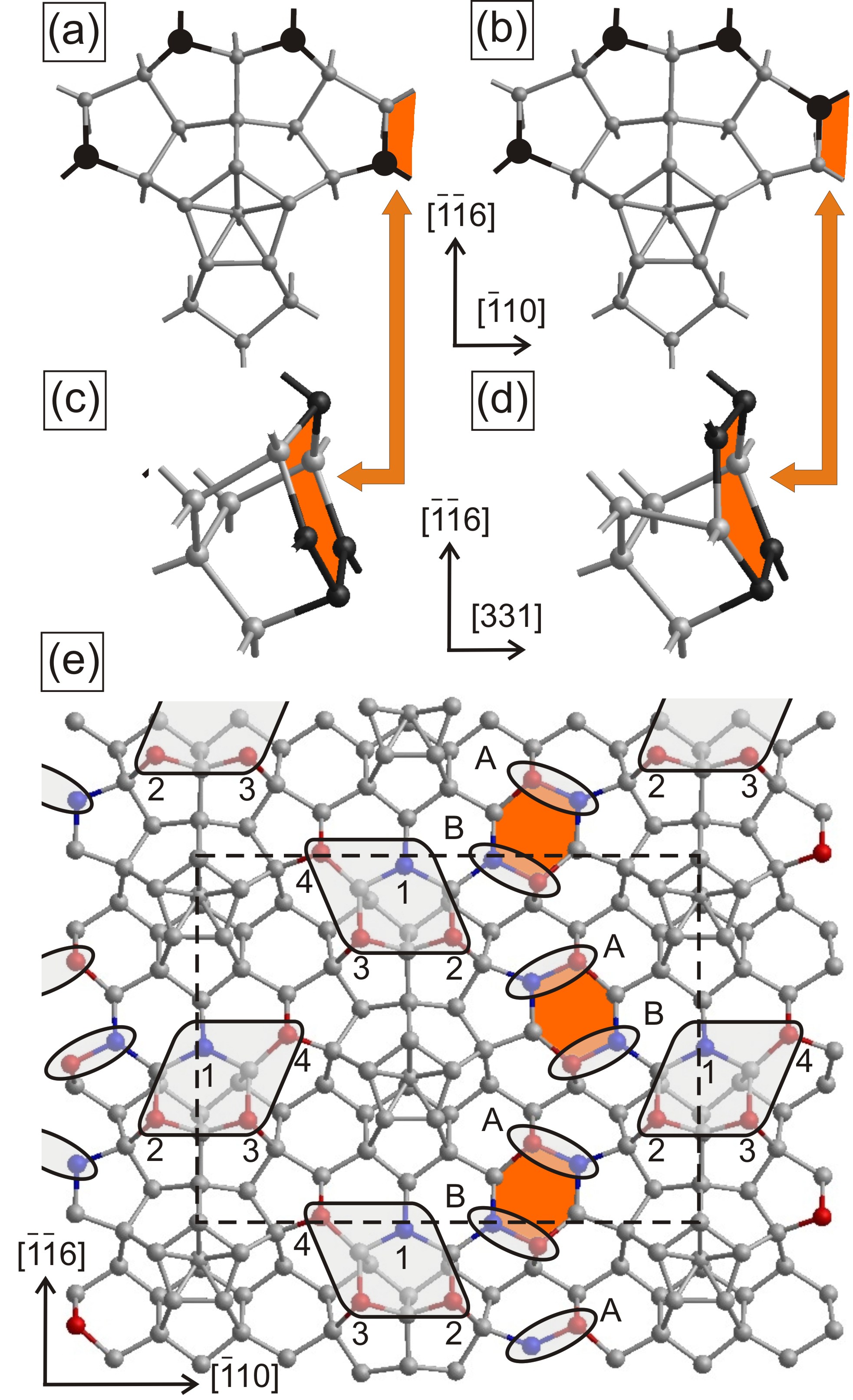
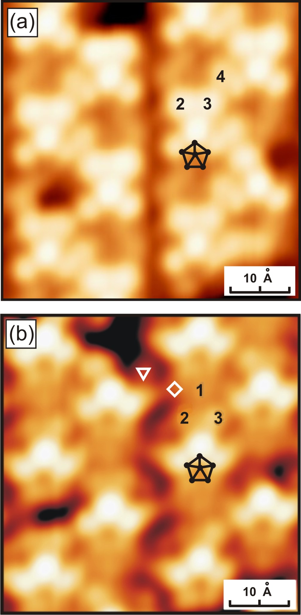
The structure of the 8-pentagon unit (8PU), proposed as the main structural building block of the Si surface,(Zhachuk and Teys, 2017) is shown in Fig. 1. The structure has mirror symmetry in the vertical plane ( direction). This is also valid for the arrangement of under-coordinated Si atoms in 8PU (black-filled circles in Fig. 1(a)). The revised version of 8PU is shown in Fig. 1(b). The difference between the original and revised versions is that the arrangement of under-coordinated Si atoms within the 8PU in Fig. 1(b) is not symmetric. The transformation from the atomic configuration shown in Fig. 1(a) into that shown in Fig. 1(b) consists of the simultaneous bond breaking (formation) between the upper (lower) atom in the right-hand side of 8PU and the Si atom in the deeper layer (see Figs. 1(c) and 1(d)). According to the revised 8P model of the Si surface, the rebonded sides of 8PUs are facing the trenches between the pentamers which are observed as dark vertical stripes in experimental STM images (Figs. 2(a) and 2(b)).
The location of the revised 8PUs on the reconstructed Si surface is shown in Fig. 1(e). Due to the rebonded Si atoms in 8PU described above, the trench between 8PUs in the revised surface model contains Si buckled dimers only. They are highlighted by ovals in Fig. 1(e). There are three main reasons for revising the 8PU structure. First, the surface energy of the Si with the revised 8PUs, shown in Fig. 1(c), is () lower than that of the original 8PUs reported in Ref. Zhachuk and Teys, 2017. Second, the original 8PUs fail to reproduce the weak spots in the STM images of the trenches, marked by the white down triangle in Fig. 2(b) (see the Appendix for the calculated STM images according to the original 8P model). These spots are clearly seen in the experimental STM images available in the literature.(Battaglia et al., 2009a; Teys, 2017) Such a limitation in the original 8PU model stems from the Si atoms on the positions, which being fully coordinated, become virtually invisible in STM. This effect is accounted for by the revised 8PU. The third reason is an excellent agreement between the spectroscopy data(Battaglia et al., 2011) and the calculated surface band gap for Si when using the revised 8P model, as shown is Section III.3. Conversely, the original 8P model proposed in Ref. Zhachuk and Teys, 2017 shows a non-zero DOS in the middle of the band gap (see the Appendix section for the calculated DOS according to the original 8P model).
As already noted in Ref. Zhachuk and Teys, 2017, the 3-fold coordinated atoms of the Si(331) surface buckle by shifting either out of the surface or into it. The lowest energy buckled configuration of the Si surface with the revised 8PUs is shown in Fig. 1(e). The protruded and depressed atoms are marked by red and blue balls, respectively. The surface unit cell contains two sets of identical reconstruction elements (8PUs with surroundings). The structural parts, which are prone to buckling, include four atom units (FAUs) and two types of dimers highlighted by rhombs and ovals in Fig. 1(e).
| Configuration | |||||
| 1 | nnnn-nn | 0 (0) | 0.33 | 3 | 0.29 |
| 4 | 0.21 | ||||
| 2 | nnnn-ff | 1.8 (57.6) | 0.23 | 3 | 0.01 |
| 3 | nnnn-nf | 1.4 (44.8) | 0.26 | 1 | 0.03 |
| 2 | 0.09 | ||||
| 4 | fnfn-nn | 0.8 (25.6) | 0.17 | 1 | 0.06 |
| 5 | ffnf-fn | 2.2 (70.5) | 0.07 | No data | |
| 6 | ffnf-ff | 2.8 (89.7) | 0.10 | No data | |
| 7 | ffnf-nf | 3.1 (99.3) | 0.11 | No data | |
We have studied the relative surface energies of different buckled configurations of Si and the energy barriers separating them. The results are given in Table 1. The energy barriers reported in Tab. 1 assume the transformation of one of the two 8PUs with the surroundings, while the second 8PU in the unit cell remains unchanged. The energy barriers are calculated by constructing 5 intermediate stages between two chosen buckled states and linear interpolating all atomic coordinates between them. The number of intermediate structures was large enough, and a smooth energy profile across neighboring images was obtained. This procedure guarantees that the value of the real energy barrier is below the calculated one. Moreover, test calculations show that the values of the energy barriers obtained using the linear interpolation of atomic coordinates are very close to that calculated using the nudged elastic band method.(Henkelman et al., 2000) This is due to the short distances between end-structures in the configurational space. For the gentle atomic transformation like buckling considered in this work, the difference between the energy barrier values calculated using the two methods does not exceed .
We have explored all possible buckled configurations within the same topology of covalent bonds, as shown in Fig. 1(c). The stable buckled configurations found in this study are listed in Table 1. Accordingly, the calculated energy barriers separating different buckled configurations are all below .
It is possible to estimate how high the kinetic barriers have to be in order make buckled configurations stable at specific operating temperatures. To that end we make use of the frequency of thermally activated switching of the buckled state using an Arrhenius relation , where , and stand for the Boltzmann constant, sample temperature and attempt frequency, which can be approximated by the Debye frequency of Si . Assuming stable structures as those flipping slower than , we define a threshold energy barrier, , below which the structure flips at a rate faster than 1 Hz. Hence, at room temperature , liquid nitrogen temperature and liquid helium temperature , the corresponding threshold energy barriers are , and .
Considering that eV, similarly to the behavior of dimers on the Si surface, we expect that both FAU atoms and dimers on Si(331) should buckle dynamically at room temperature due to the thermally activated motion of atoms.(Hamers et al., 1986) On the other hand, the energy barrier separating the original 8PU from the revised 8PU shown in Figs. 1(a) and (b), respectively, which involves the breaking and formation of covalent bonds, is significantly higher (). Therefore, we may expect that a spontaneous rebonding on the Si surface at room temperature is less likely.
III.2 Atomic orbitals for the calculation of bias-dependent STM images
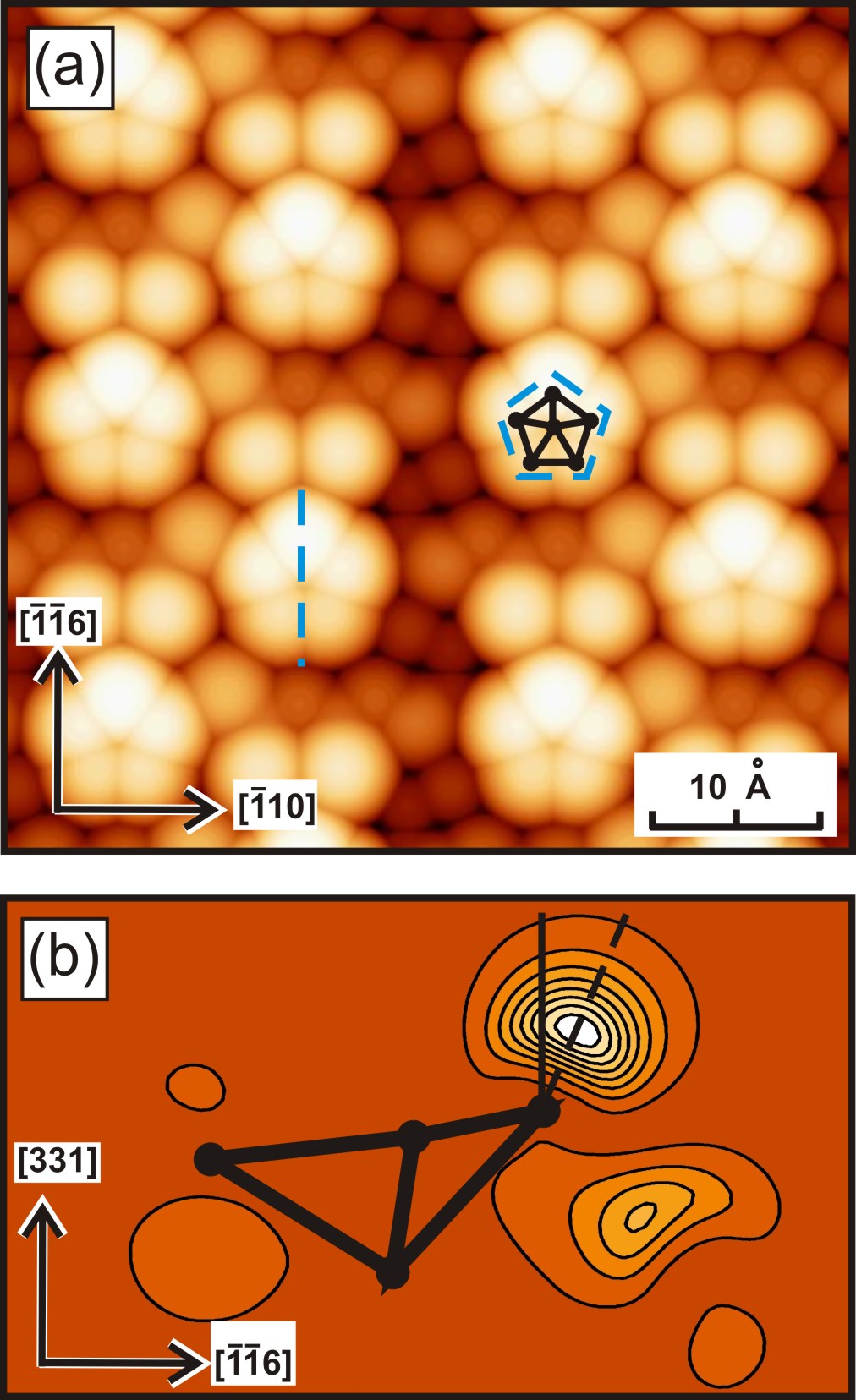
Figure 3(a) shows the calculated constant-current STM image of the Si according to the revised 8P model of Fig. 1(c). The standard bulk-optimized DZP basis set was used for Si surface atoms. The structure of the pentamer with an interstitial atom is also overlaid in Fig. 3(a). The actual distance between the nearest Si atoms in the pentamer is . The dashed blue pentamer in Fig. 3(a) emphasizes its apparent size as derived from the calculated STM image. The distance between two nearest spots is about , in agreement with the analogous distance as derived from the experimental STM image of Fig. 2(b). On the other hand this figure corresponds to a deviation of more than 50% with respect to the atomic positions according to the 8P model. Such a size mismatch sustained an argument against the atomic models of silicon surface involving five-fold rings of Si atoms.(Teys, 2017) It should be noted, however, that STM is a technique sensitive to LDOS, rather than the positions of atomic nuclei.(Tersoff and Hamann, 1985)
Figure 3(b) shows a vertical cut of the integrated LDOS (between +0.8 V and Fermi level) along the blue dashed segment crossing the pentamer in Fig. 3(a), combined with a projection of a pentamer atomic structure. The brightest spot at the upper right corner of Fig. 3(b) shows a high intensity for the empty LDOS located near the Si radical at the upmost apex of the pentamer in Fig. 3(a). Clearly, the radical state does not point upwards (along ), rather making an angle of about 22° with respect to the surface normal and away from the center of the pentamer. Since STM is intrinsically sensitive to LDOS(Tersoff and Hamann, 1985) and because the tip usually scans between 4 to 10 Å above the surface,(Hofer, 2003) it becomes evident that the slanted radicals will project a magnified image of the underlying pentamer. This explains the apparent contradiction between the size of the pentamers from the atomistic model and those derived directly from STM images (see Ref. Teys, 2017).
The main advantage of using atomic orbitals as a basis set resides on their efficiency (fewer orbitals per state are needed in order to obtain a precision similar to that of plane-wave codes). However, there are also known issues when atomic orbitals are used for the calculation of the surface properties, such as surface formation energies, surface state energies and work functions.(García-Gil et al., 2009) In this paper, we show that, in addition to the problems listed above, the calculated STM images may show no bias dependency because of the short decay length of the basis functions into the vacuum space. However, we demonstrate that an accurate description of the STM images is, nevertheless, possible with an appropriately tuned basis set.
First, we note that although spot positions in the calculated STM image of Fig. 3(a) closely reproduce the spot positions in the experimental STM images (Figs. 2(a) and 2(b)), their relative intensities are incorrect. Second, the positive and negative bias STM images calculated using the standard bulk-optimized DZP basis set are almost undistinguishable, while the experimental STM images show a strong bias-dependency (Figs. 2(a) and 2(b)).(Teys, 2017) The height contrast measured from the calculated STM image shown in Fig. 3(a) mostly represents the surface topography. It lacks the electronic contribution, closely matching the height differences measured from Si nuclei positions.
The Sankey-Niklewski-type orbitals used in the siesta code are the eigenfunctions of the (pseudo) atom within a sphere of cut-off radius R (orbitals are strictly zero beyond this radius).(Soler et al., 2002) Thus, the orbitals are obtained as a product between a confined radial function and a spherical harmonic. In order to describe the properties of the surfaces accurately, one needs to include orbitals which can describe the long decay of the wave functions.
Three different schemes were proposed in Ref. García-Gil et al., 2009. First is to add diffuse functions (with a longer cut-off than that of the bulk-optimized orbitals) to the basis. According to our test calculations, this scheme leads to improved calculated STM images. However, the overlap of the extra orbitals with the orbitals of the original bulk-optimized basis set leads to artifacts in calculated images. Another scheme is to add a set of floating orbitals (ghost atoms) located above the surface. These are off-site orbitals centered at the points where there are no atoms. The problem with this scheme is that, on the reconstructed surfaces, such as the one shown in Fig. 1(e), there is no obvious and unbiased way for their placement. The resulting STM images also show artifacts which additionally depend on the placement of off-site orbitals.
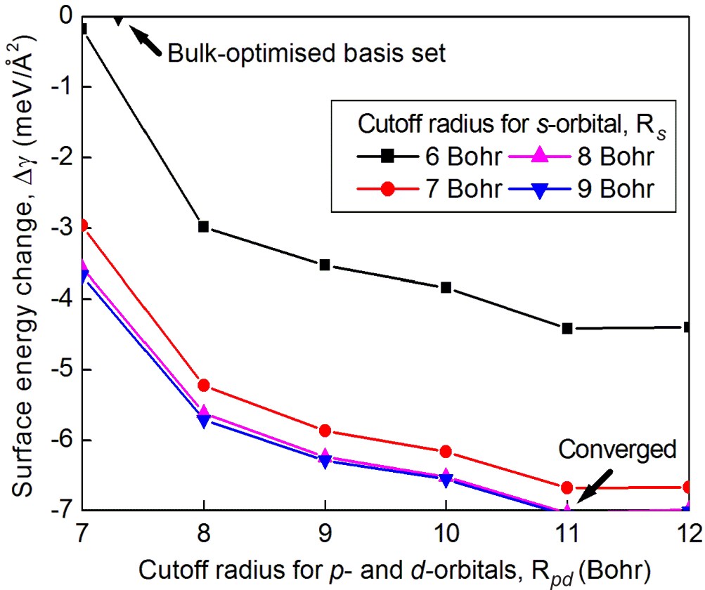
The last scheme is to enlarge the cut-off radius of the atomic orbitals at the surface layer atoms only, which allows the wave functions to spread further into vacuum. Increasing the orbital cut-off radii at the surface atoms leads to the basis functions with the natural decay of the atomic orbitals in the free atom which greatly improves the description of the surface properties.(García-Gil et al., 2009) The confinement radii for the atoms in the two upper bilayers of the slab were taken as a variational parameter to optimize the quality of the basis set and are chosen to minimize the slab total energy. The radii for s- and p-orbitals ( and ) were varied independently, while the radius for the d-orbital was set equal to that of the p-orbital (). The change of the slab total energy is represented as corresponding change of the relative surface energy in Fig. 4. According to that figure, the total energy of the slab shows a noticeable reduction when the confinement radii are increased, and that clearly indicates the need to expand the basis to describe properly the vacuum region. The energy converges at about and (Fig. 4). The bias-dependent STM images in Figs. 5(a) and 5(b) are calculated using the DZP basis set optimized for the surface according to the described procedure. These images closely reproduce the bias dependence of the experimental STM images in Figs. 2(a) and 2(b), and that strongly supports the revised 8P model for the Si surface. The STM images for the lowest energy configuration were also calculated using the vasp code and within the GGA to the exchange-correlation interactions, essentially resulting in identical STM images as those in Figs. 5(a) and 5(b) (not shown).
It is interesting to compare the absolute surface energy calculated using the standard bulk-optimized DZP basis with that calculated using the surface-optimized DZP basis, as well as with a well-converged PW calculation. The absolute surface energy of the unreconstructed and unrelaxed Si surface is when using the PW code.(Battaglia et al., 2009b) We used a 14 bilayers thick symmetric slab to calculate the formation energy of the same surface using a strictly localized DZP basis set. We found that the formation energy of that surface is when using the standard bulk-optimized basis set, while it is when using the surface-optimized basis. Thus, besides improving significantly the quality of the calculated STM images, the surface-optimized basis improves the absolute surface formation energy, leaving the relative surface energies essentially unchanged (see Tab. 1).
III.3 Origin of STM contrasts and electronic structure of the Si(331)-(12×1) surface
In figures 5(a) and 5(b) we depict the calculated STM images of the Si surface assuming the revised 8P model for the reconstruction. The surface-optimized basis set is used for two upper bilayers of the slab and the lowest energy buckled configuration shown in Fig. 1(e) is assumed. The images were calculated using a tip-surface separation of about Å (as measured from the topmost point of the LDOS isosurface to the highest point of the Si lattice). We found that the dependence of the STM images on the tip-surface separation is weak, with spots becoming more diffuse as the distance increased within the range Å (setting different LDOS isosurfaces). The positive and negative bias STM images differ from each other in relative intensity of spots. This is in agreement with the experimental STM images shown in Figs. 2(a) and 2(b) (Ref. Teys, 2017), providing compelling evidence of a strong contribution of the electronic states to the observed STM height contrast.
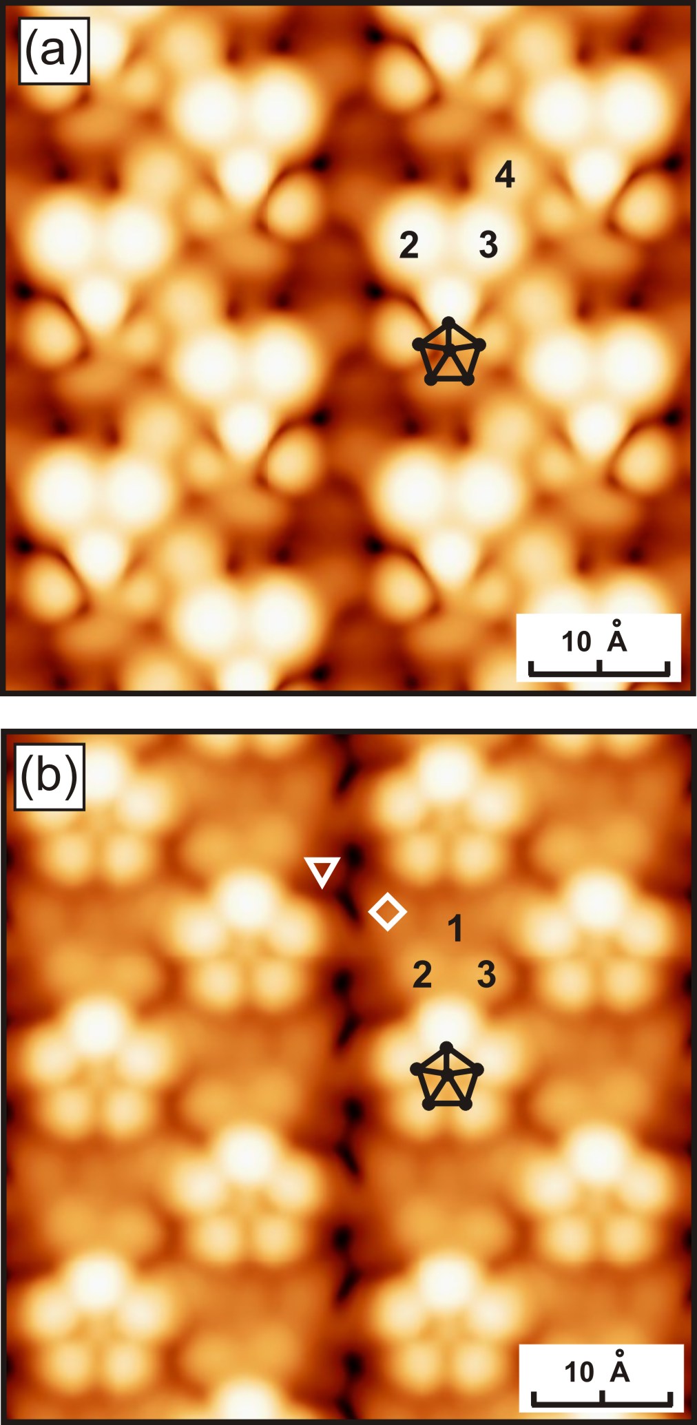
There is a clear similarity between the experimental and calculated STM images shown in Figs. 2(a), (b) and Figs. 5(a), (b), respectively. The calculated STM image of the pentamer with an interstitial atom shows 5 bright spots at positive bias (Fig. 5(b)) and 4 spots at negative bias (Fig. 5(a)) in agreement with the bias-dependent experimental STM images of the pentamers on the Si surface.(An et al., 2000) The experimental STM image of the pentamer on the Si surface shows 5 distinct spots at the positive bias (Fig. 2(b)), while only 3 spots are visible in the negative bias (Fig. 2(a)). We should note here that our calculated positive bias STM images are closer to the images reported by Battaglia et al. in Refs. Battaglia et al., 2009a, b, 2011 than to the images reported by Teys in Ref. Teys, 2017. The difference between experimental STM images by different authors can, in principle, be explained by variations in the quality of the STM tips, which is hard to control in experiments. We, therefore, suggest that the small difference observed between the experimental and calculated STM images in Figs. 2(a) and Figs. 5(a) could be due to the STM tip. In other words, the 4-th banana-shaped spot observed in the calculated STM image of the pentamer in Fig. 5(a), is simply unresolved in the experimental STM image of Fig. 2(a).
Depending on the applied bias polarity, different spots are highlighted in the STM images of FAU (Figs. 2 and 5). These spots are numbered according to the scheme shown in Fig. 1(e). In the STM images with a negative bias (filled electronic states), spots 2, 3 and 4 are bright, while spot 1 is dimmed (Figs. 2(a) and 5(a)). In the STM images with a positive bias (empty electronic states), spots 1, 2 and 3 can be distinguished, while spot 4 is less visible (Figs. 2(b) and 5(b)). Thus, the relative change of the spot brightness in the experimental STM images of FAUs upon reversing the bias polarity is reproduced in the theoretical STM images.
Few weak spots are visible in the trench observed as a dark vertical stripe in the middle of the experimental STM image of Fig. 2(b). These spots are marked by a white rhomb and triangle. According to the revised 8P model shown in Fig. 1(e), these spots originate from the buckled dimers located in the trenches between the pentamers. The spots are well reproduced in the calculated STM image assuming the revised 8P model for the Si surface in Fig. 5(b). The remaining small differences between the experimental and calculated STM images might be explained by the dynamic buckling of dimers and FAUs and, therefore, by considering the contributions from other (higher energy) buckled configurations listed in Tab 1.
According to the Tersoff-Hamann approximation, the STM images represent a combination of surface topography and a map of the sample surface LDOS.(Tersoff and Hamann, 1985; Hofer, 2003) It is therefore interesting to plot LDOS isosurfaces in order to isolate the electronic contribution to the STM images. Figure 6 shows the calculated LDOS isosurfaces integrated over a window just below (a) and above (b) the calculated Fermi level (filled and empty electronic states, respectively). The lowest energy buckled configuration shown in Fig. 1(e) is assumed. These results were obtained within hybrid DFT (using the HSE06 functional), allowing a direct comparison with the DOS data of Figure 7 below. One can see that the filled and empty LDOS images are fully complementary.
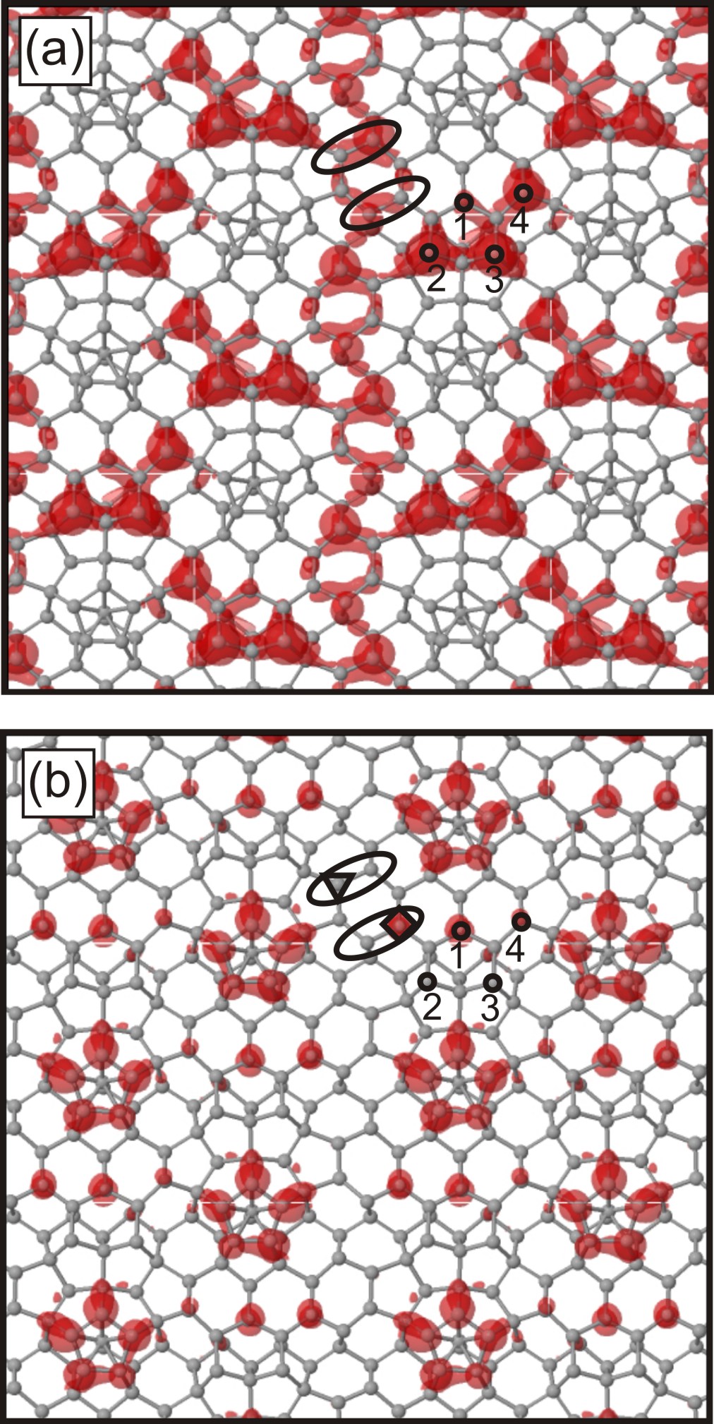
The empty LDOS are located on the pentamer atoms and 3-fold coordinated atoms having the sp2-like (planar) configuration of their bonds. These latter atoms correspond to the depressed atoms in the buckled configuration shown in Fig. 1(e). The filled LDOS are located on the 3-fold coordinated atoms showing sp3-like configurations of their bonds (both in FAUs and on the protruded dimer atoms in the trench). These atoms correspond to the protruded atoms in the buckled configuration shown in Fig. 1(e). The overall redistribution of electron density from the sp2-like to sp3-like Si surface atoms is in agreement with the observations made on and silicon surfaces.(Bechstedt, 2003; Zhachuk et al., 2014)
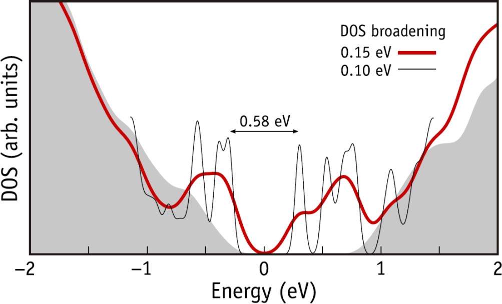
Finally, we studied the band structure of the Si reconstructed surface using hybrid DFT. This allows us to make a direct comparison with the spectroscopic data involving the energies in the range of the band gap. Again, as in the case of STM images, we consider only the lowest energy buckled configuration shown in Fig. 1(e) (first configuration in Tab. 1). Due to the sparse nature of the electronic states within the gap (as evidenced by Fig. 6), the bands show very weak dispersion (not shown here). The calculated total DOS is plotted in Fig. 7. The spectrum shows two broad peaks, when using a broadening (thick red line): one above the valence band maximum, and another one below the conduction band minimum. The calculated band gap for the surface is eV, which is almost twice the value obtained using LDA (Table 1). The shape of the 0.15 eV broadened DOS spectrum and the calculated value of the band gap are in a very good agreement with the experimental analogues from angle-resolved photoelectron and scanning tunneling spectroscopy (STS). These also show two broad peaks edging the band gap, whose width was estimated between and .(Battaglia et al., 2011)
Concerning the broadening of the DOS peaks, we note that the error of the DOS should be close to that of the calculated gap within hybrid DFT as reported in Section II, which is about eV. The thermal smearing due to finite temperature (at room temperature) is about eV. Both these values are lower than the eV peak smearing of Fig. 7, therefore accounting for the broadening due to experimental conditions. The typical STS resolution is about eV, while some disorder on the Si surface and dynamic buckling will contribute to a smeared spectrum (c.f. reported LDA band gaps in Tab. 1). The broad peaks calculated at eV smearing hide a fine structure when the spectrum is calculated using a eV broadening (thin black line). This finer spectrum is given for guidance, hoping for a future improvement in equipment resolution and sample quality.
IV Conclusions
In summary, the Si surface reconstruction was studied theoretically using density functional calculations, and the results were compared to the available experimental data. We propose important correction to the 8P structural model of the Si reconstructed surface, suggesting that the trenches between the zig-zag chains of 8PUs consist of dimers. It is demonstrated that an accurate description of the bias-dependent STM images and energetics of the reconstructed surface is possible using a basis set consisting of atomic orbitals. The apparent contradiction between the size of the pentamers from the atomistic model and those derived directly from STM images is explained within the context of the Tersoff-Hamann model. The revised 8P model of the Si reconstructed surface shows a remarkable agreement with the experimental STM images, spectroscopy data and the width of the surface band gap. The calculated energy barriers separating different buckled configurations of the Si surface assume that this surface is prone to dynamic buckling at room temperature. Overall, the presented results demonstrate that the revised 8P model of the Si reconstructed surface is in a very good agreement with the available experimental data and, therefore, it can serve as a reliable starting point for future research studies related to this surface.
Acknowledgements.
We would like to thank the Novosibirsk State University for providing the computational resources. R. Zhachuk acknowledges the financial support of the Russian Foundation for Basic Research (Project No. 18-02-00025). This work was partially funded by the Fundação para a Ciência e a Tecnologia (FCT) under the contract UID/CTM/50025/2013 and by FEDER funds through the COMPETE 2020 Program. Partial funding was also provided by the Slovak Academy of Sciences SASPRO program 1239/02/01, and by the National Research Development and Innovation Office of Hungary project FK124100.APPENDIX: Calculated STM images and DOS of the original 8P model
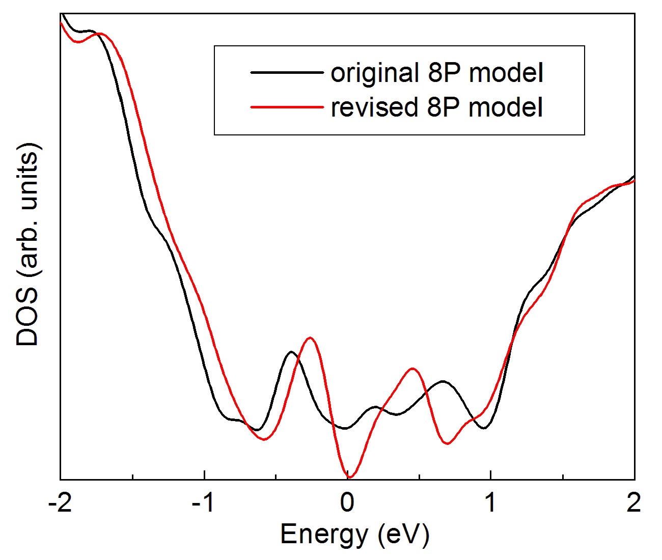
In this section we show calculated STM images (Fig. 8) and DOS (Fig. 9) of the original 8P model for the Si surface, as proposed in Ref. Zhachuk and Teys, 2017. Figure 9 compares the DOS for the original and the newly proposed 8P models. Both calculations were carried out using the siesta code within the LDA to the exchange-correlation energy.
Figures 8(a) and 8(b) show the calculated STM images of the Si surface assuming the original 8P model for the reconstruction, proposed in Ref. Zhachuk and Teys, 2017. The surface-optimized DZP basis set used for the revised model shown in Fig. 5 is used in this case as well. The calculated STM image in Fig. 8(a) shows that the relative intensity of spots in FAUs does not match the relative intensity of spots in corresponding experimental STM image in Fig. 2(a). More importantly, the spot marked by a down triangle in the experimental STM image in Fig. 2(b) is completely absent in the calculated STM image of Fig. 8(b).
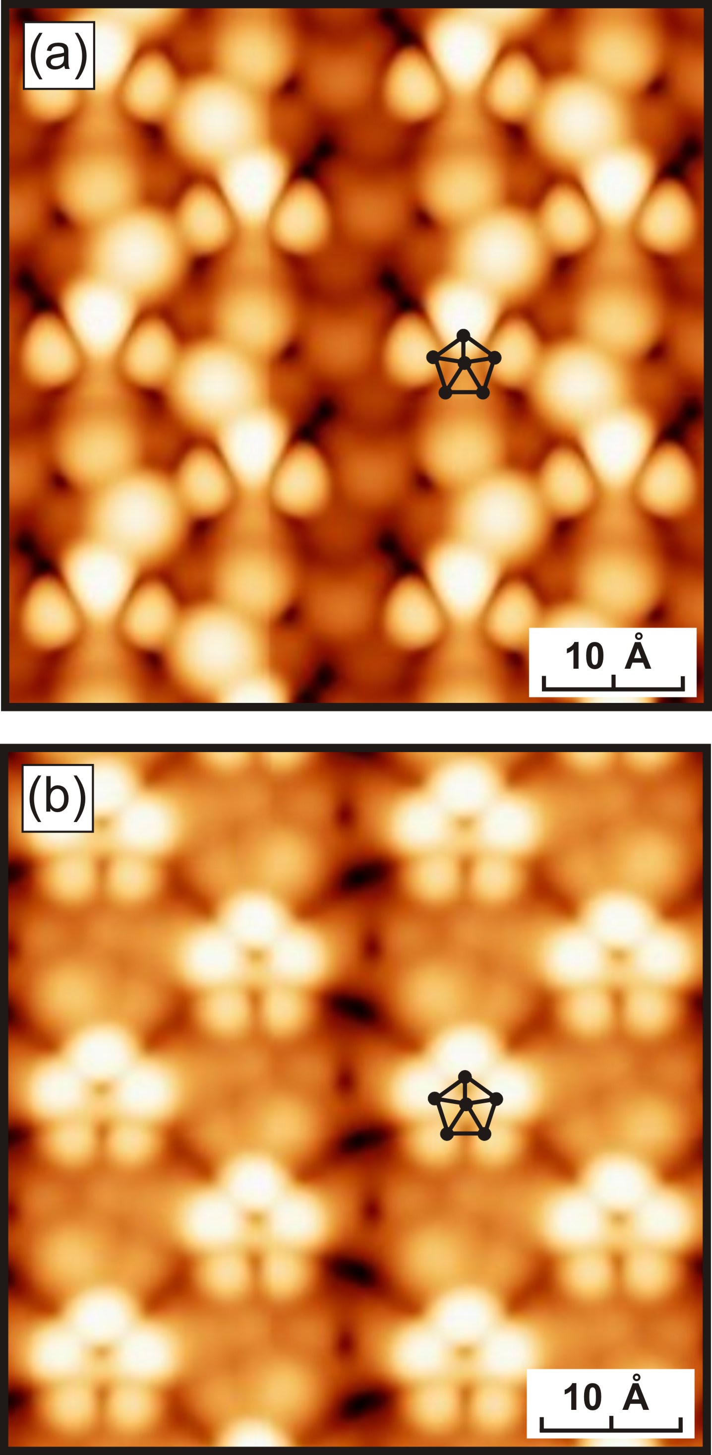
Figure 9 shows the calculated DOS spectra according to the original (black line) and revised (red line) 8P models of the Si surface, respectively. The DOS spectrum calculated using the original 8P model shows a non-vanishing DOS amplitude in the region of the Fermi energy ( eV), at variance with the experimental data.(Battaglia et al., 2011)
Hence, Figs. 8 and 9 demonstrate that the original 8P model for the Si surface cannot account for the observations, unlike the revised 8P model.
References
- Sagisaka et al. (2003) K. Sagisaka, D. Fujita, and G. Kido, Physical Review Letters 91, 146103 (2003).
- Takagi et al. (2004) Y. Takagi, M. Yamada, K. Nakatsuji, and F. Komori, Applied Physics Letters 84, 1925 (2004).
- Zhachuk and Teys (2017) R. Zhachuk and S. Teys, Physical Review B 95, 041412(R) (2017).
- Zhachuk et al. (2014) R. Zhachuk, S. Teys, J. Coutinho, M. J. Rayson, and P. R. Briddon, Applied Physics Letters 105, 171602 (2014).
- Zhachuk et al. (2004) R. A. Zhachuk, S. A. Teys, A. E. Dolbak, and B. Z. Olshanetsky, Surface Science 565, 37 (2004).
- Teys et al. (2006) S. A. Teys, K. N. Romanyuk, R. A. Zhachuk, and B. Z. Olshanetsky, Surface Science 600, 4878 (2006).
- Olshanetsky and Mashanov (1981) B. Z. Olshanetsky and V. I. Mashanov, Surface Science 111, 414 (1981).
- Battaglia et al. (2009a) C. Battaglia, K. Gaál-Nagy, C. Monney, C. Didiot, E. F. Schwier, M. G. Garnier, G. Onida, and P. Aebi, Physical Review Letters 102, 066102 (2009a).
- Teys (2017) S. A. Teys, JETP Letters 105, 477 (2017).
- Wood (1964) E. A. Wood, Journal of Applied Physics 35, 1306 (1964).
- Hibino and Ogino (1996) H. Hibino and T. Ogino, Physical Review B 53, 15682 (1996).
- Olshanetsky et al. (1998) B. Z. Olshanetsky, S. Teys, and I. G. Kozhemyako, Phys. Low-Dim. Struct. 11/12, 85 (1998).
- Gai et al. (2001) Z. Gai, R. G. Zhao, T. Sakurai, and W. S. Yang, Physical Review B 63, 085301 (2001).
- Soler et al. (2002) J. M. Soler, E. Artacho, J. D. Gale, A. García, J. Junquera, P. Ordejón, and D. Sánchez-Portal, J. Phys.: Condens. Matter 14, 2745 (2002).
- Kresse and Hafner (1993) G. Kresse and J. Hafner, Physical Review B 47, 558 (1993).
- Kresse and Hafner (1994) G. Kresse and J. Hafner, Physical Review B 49, 14251 (1994).
- Kresse and Furthmüller (1996a) G. Kresse and J. Furthmüller, Physical Review B 54, 11169 (1996a).
- Kresse and Furthmüller (1996b) G. Kresse and J. Furthmüller, Computational Materials Science 6, 15 (1996b).
- Perdew and Wang (1992) J. P. Perdew and Y. Wang, Physical Review B 45, 13244 (1992).
- Troullier and Martins (1991) N. Troullier and J. L. Martins, Physical Review B 43, 1993 (1991).
- Zhachuk et al. (2013) R. Zhachuk, S. Teys, and J. Coutinho, Journal of Chemical Physics 138, 224702 (2013).
- Monkhorst and Pack (1976) H. J. Monkhorst and J. D. Pack, Physical Review B 13, 5188 (1976).
- Tersoff and Hamann (1985) J. Tersoff and D. R. Hamann, Physical Review B 31, 805 (1985).
- Horcas et al. (2007) I. Horcas, R. Fernández, J. M. Gómez-Rodríguez, J. Colchero, J. Gómez-Herrero, and A. M. Baro, Review of Scientific Instruments 78, 013705 (2007).
- Heyd et al. (2003) J. Heyd, G. E. Scuseria, and M. Ernzerhof, Journal of Chemical Physics 118, 8207 (2003).
- Krukau et al. (2006) A. V. Krukau, O. A. Vydrov, A. F. Izmaylov, and G. E. Scuseria, The Journal of Chemical Physics 125, 224106 (2006).
- Battaglia et al. (2011) C. Battaglia, E. F. Schwier, C. Monney, C. Didiot, N. Mariotti, K. Gaál-Nagy, G. Onida, M. G. Garnier, and P. Aebi, Journal of Physics: Condensed Matter 23, 135003 (2011).
- Perdew et al. (1996) J. P. Perdew, K. Burke, and M. Ernzerhof, Physical Review Letters 77, 3865 (1996).
- Blöchl (1994) P. E. Blöchl, Physical Review B 50, 17953 (1994).
- Kresse and Joubert (1999) G. Kresse and D. Joubert, Physical Review B 59, 1758 (1999).
- Henkelman et al. (2000) G. Henkelman, B. P. Uberuaga, and H. Jónsson, The Journal of Chemical Physics 113, 9901 (2000).
- Hamers et al. (1986) R. J. Hamers, R. M. Tromp, and J. E. Demuth, Physical Review B 34, 5343 (1986).
- Bechstedt (2003) F. Bechstedt, Principles of surface physics (Springer, 2003).
- Hofer (2003) W. A. Hofer, Progress in Surface Science 71, 147 (2003).
- García-Gil et al. (2009) S. García-Gil, A. García, N. Lorente, and P. Ordejón, Physical Review B 79, 075441 (2009).
- Battaglia et al. (2009b) C. Battaglia, G. Onida, K. Gaál-Nagy, and P. Aebi, Physical Review B 80, 214102 (2009b).
- An et al. (2000) T. An, M. Yoshimura, I. Ono, and K. Ueda, Physical Review B 61, 3006 (2000).