Intersubband plasmon excitations in doped carbon nanotubes
Abstract
We theoretically investigate intersubband plasmon excitations in doped single wall carbon nanotubes (SWNTs) by examining the dependence of plasmon frequency on the nanotube diameter, chirality, and Fermi energy. The intersubband plasmons can be excited by light with polarization perpendicular to the nanotube axis and thus the plasmon excitations corresponds to optical transitions between the two different subbands, which are sensitive to the Fermi energy. In every SWNT, this mechanism leads to the emergence of the optical absorption peak at the plasmon frequency for a given Fermi energy, . The plasmon frequencies calculated for many SWNTs with diameter nm exhibit a dependence on and the frequencies are further affected by Fermi energy as . With this knowledge, it is possible to develop a map of intersubband plasmon excitations in doped SWNTs that could be useful to quickly estimate the doping level and also be an alternative way to characterize nanotube chirality.
I Introduction
For many years, single wall carbon nanotubes (SWNTs) have been an important platform to study optical properties of one-dimensional (1D) materials, especially due to their geometry-dependent optical absorption Kataura et al. (1999); Saito et al. (2000); Bachilo et al. (2002); Weisman and Bachilo (2003) and also due to their potential applications for optoelectronic devices Avouris et al. (2006, 2008); Kaskela et al. (2010); Tsapenko et al. (2018). Of the wide interests in the optical properties of SWNTs, a particular problem of the doping effects on the absorption of linearly polarized light is worth investigating. So far, previous studies have confirmed that undoped SWNTs absorb only light with polarization parallel to the nanotube axis Ajiki and Ando (1994); Hwang et al. (2000); Jiang et al. (2004); Murakami et al. (2005); Li et al. (2001), so that when the light polarization is perpendicular to the nanotube axis the undoped SWNTs do not show any absorption peak due to the depolarization effect Uryu and Ando (2006); Jiang et al. (2004). The optical absorption in the case of parallel polarization can be understood in terms of the interband excitations from the ith valence to the ith conduction energy subbands, either in single-particle Ajiki and Ando (1994); Saito et al. (2000); Jiang et al. (2004) or excitonic picture Spataru et al. (2004); Wang (2005); Dukovic et al. (2005); Jiang et al. (2007). On the other hand, much uncertainty still exists about what happens in the case of doped SWNTs for the linearly polarized light.
Recently, Sasaki et al. suggested that doped (undoped) SWNT absorb light with polarization perpendicular (parallel) to the nanotube axis Sasaki et al. (2016); Sasaki and Tokura (2018). Furthermore, Yanagi et al. Yanagi et al. (2018) experimentally gave evidence that the doped SWNTs absorb light with the perpendicular polarization within the near-infrared range of a photon energy (– eV). This energy range is similar to that when undoped SWNTs absorb light with the parallel polarization. Senga et al. showed consistent absorption peaks for isolated metallic SWNTs that are unintendedly doped on the TEM supporting grid during electron energy-loss spectroscopy (EELS) measurement Senga et al. (2016, 2018). Yanagi et al. proposed that the absorption peaks are related with intersubband plasmon excitations Yanagi et al. (2018), i.e., the optical transitions with energies occur collectively between two electronic subbands and as a response to the perpendicularly polarized light. Unlike the interband excitations which take place from the valence to the conduction bands, the intersubband plasmon excitations occur within the conduction band or within the valence band.
It should be noted that in the EELS experiment by Senga et al. we can also see another plasmonic peak around , the so-called plasmon, which is not excited by light with perpendicular polarization but with parallel polarization Senga et al. (2016, 2018). Observations of the -plasmons in SWNTs Kuzuo et al. (1992, 1994) or any graphitic materials Papagno and Caputi (1983); Liou et al. (2014); Hu et al. (2014), either doped or undoped, are quite common in the earlier EELS experiments and the peaks are assigned unambiguously. Lin and Shung in two decades ago theoretically explained the origin of plasmons in the SWNTs as a result of collective interband excitations of the -band electrons Lin and Shung (1994); Lin et al. (1996). On the other hand, the theory for plasmons excited in doped SWNTs with perpendicularly polarized light is just available recently by Sasaki et al. Sasaki et al. (2016); Sasaki and Tokura (2018) and Garcia de Abajo de Abajo (2014), in which they discussed how the plasmon frequency ) in a doped SWNT depends on its diameter () and Fermi energy (). However, the dependence of on and was analyzed within the Drude model, which is not relevant to intersubband transitions but it deals with intrasubband transitions. In this sense, there is a necessity to properly describe the intersubband plasmons in the doped SWNTs for any SWNT structure or chirality.
In this work, we show our calculation of plasmon frequencies for the doped SWNTs as a function of diameter and the Fermi energy, considering all SWNTs with different chiralities in the range of nm. The calculated plasmon frequencies exhibit a diameter dependence of and are further dependent on the Fermi energy as . This scaling of plasmon frequency differs with that predicted by the Drude model, Sasaki et al. (2016); de Abajo (2014), hence indicating the difference of the intersubband transitions (current work) from the intrasubband transitions (the Drude model). We further consider optical absorption at the plasmon frequencies caused by intersubband transitions within the conduction and valence bands, corresponding to and , respectively. We find that the most dominant plasmonic transition, which we label as at a certain energy (following the notation introduced by Bondarev Bondarev (2012) for the interband plasmon at ), changes with Fermi energy from a to another . For the smaller (larger) nanotube diameter, we need higher (lower) to excite the plasmon. Using the fitting formula for the plasmon frequency provided in this paper, one can estimate the Fermi energy in the doped SWNTs by means of optical spectroscopy, as well as EELS. Furthermore, experimentalists can also search for intersubband plasmons in isolated SWNTs with various chiralities, not only limited to SWNTs bundles.
The rest of this paper is organized as follows. In Sec. II, we describe how to calculate the plasmon frequency for a given SWNT starting from the dielectric function of the SWNT. The complex dielectric function in this work is calculated within the self-consistent-field approach by considering dipole approximation for optical matrix elements, from which there exist selection rules for different light polarization. In Sec. III, we discuss the main results of intersubband plasmon frequencies, including the opportunity to map them into a unified picture of . We justify the fitting by means of graphene plasmon dispersion, considering the model of the rolled graphene sheet for a SWNT. Finally, we give conclusions and future perspectives in Sec. IV.
II Theoretical methods
II.1 Defining plasmons from dielectric function
We consider a SWNT subjected to perturbation by light whose vector potential, electric field, and magnetic field are denoted by , , and , respectively. The vector potential of the electric field of incident light at the position of and time is given by:
| (1) |
where , , , and denote the vector potential amplitude, angular frequency, wave vector in the direction of propagation, and unit vector of polarization direction, respectively. The magnetic and electric fields are related with by and , respectively. These quantities are important in the calculation of optical matrix elements, as derived in details in Appendix A.
We will discuss two cases of : parallel and perpendicular to the nanotube axis, shown in Fig. 1. We refer to the two cases as the parallel polarization and perpendicular polarization. The nanotube axis is denoted by the translational vector in three dimension as shown in Fig. 1(a) for and Fig. 1(b) for . If we imagine the SWNT as a rolled-up graphene sheet, the nanotube axis in the unrolled sheet is always perpendicular to the chiral vector , thus the unit cell of the SWNT is defined by the rectangular whose boundaries are and Saito et al. (1998). The chiral vector in the basis of two-dimensional (2D) lattice vectors of graphene uniquely identifies the SWNT structure by , where the set of integers is known as the chirality.
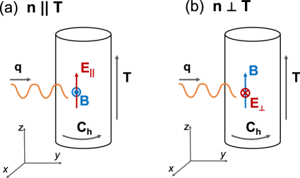
In both optical spectroscopy and EELS, plasmons are observed as prominent peaks in the spectra. The intensity of optical absorption is proportional to Helm (2000), where and are, respectively, optical conductivity and dielectric function as a function of light frequency . Note that the dielectric function in the optical absorption accounts for the depolarization effect, which means that the screening of the external electrical field is included in the calculation of optical absorption for both perpendicular and parallel polarizations of light. Indeed, the depolarization effect is essential for explaining the anisotropy of optical absorption in SWNTs Ajiki and Ando (1993); Uryu and Ando (2006); Nakanishi and Ando (2009). On the other hand, the intensity of EELS is proportional to the energy loss-function, Ritchie (1957); Raether (1980), that describes the excitation spectrum of solid by inelastic scattering of electrons at small angles. The plasmon peaks originate from zero points of the real part of , i.e., , followed by a relatively small value of its imaginary part, , in comparison with the maximum of .
According to the Maxwell equations, the optical conductivity is related to the dielectric function as follows:
| (2) |
where is surrounding dielectric permittivity ( for SWNT film Igarashi et al. (2015)) and is effective thickness of the material ( for SWNT). We calculate within the self-consistent-field approach in the following form Ehrenreich and Cohen (1959); Lin and Shung (1994):
| (3) |
where is the optical matrix element corresponding to a transition from an initial state to a final state ) Saito et al. (2004), is the cross section area of a SWNT, and is Fermi-Dirac distribution function. The electron wave function is related with the subband energy , where () for a conduction (valence) subband and is the index for the cutting line, which represents the 1D Brillouin zone (BZ) of the SWNT Saito et al. (1998) with the electron wave vector . The cutting lines are plotted in the 2D BZ of graphene with index . The value of depends on according to the formula , where .
In Eq. (II.1), is the broadening factor that accounts for relaxation processes in optical transitions resulting in finite lifetime of the electron state. Here we simply assume that does not depend on or but is constant, Hertel and Moos (2000). The numerical integration over is implemented by the left Riemann sums approximation, where the step is chosen to reach an accuracy , corresponding to , where is the Fermi velocity in graphene.
To obtain the energy band structure of carbon nanotubes, we adopt the zone-folding approximation of graphene with long-range atomic interactions up to the third nearest-neighbor transfer integrals, or the so-called third nearest-neighbor tight-binding (3rd NNTB) model Reich et al. (2002); Chegel (2015). Although this approach does not include the curvature effect, the resulting band structure is sufficiently accurate for SWNTs with diameter larger than Popov (2004). Note that in contrast to the simplest tight-binding approach, the subbands within the valence and conduction bands in the 3rd NNTB model are not further symmetric with respect to . Therefore, the SWNTs properties are more sensitive to the doping type (-type or -type) as usually observed in experiments.
II.2 Optical selection rules
Both dielectric function and optical conductivity are obtained by taking summation of different contributions from all possible pairs of and . Although the summation in Eq. (II.1) is performed over all the cutting lines in valence and conduction bands, only limited number of subbands gives nonzero contribution. The transition is contributive when is nonzero (optical selection rules) and the Pauli exclusion principle is satisfied (the difference of Fermi-Dirac distributions in Eq. (II.1) is nonzero). The concept of optical selection rules for SWNTs was originally discussed by Ajiki and Ando Ajiki and Ando (1994), who formulated the optical matrix elements by current-density operator. They proved that the allowed transitions are always vertical () and the cutting line index should be conserved for parallel polarization (). On the other hand, the optical transition for perpendicular polarization occurs within nearest neighbor cutting lines, .
For the sake of completeness, we rederive the optical selection rules within the dipole approximation. For parallel polarization, the optical matrix elements are
| (4) |
and for perpendicular polarization we obtain
| (5) |
The detailed derivation for Eqs. (II.2) and (II.2), as well as the meaning of each variable in their right-hand sides, are given in Appendix A. It should be noted that the results of optical selection rules are the same either by considering dipole approximation or current-density operator Ajiki and Ando (1994).
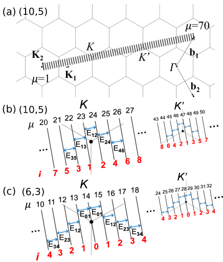
When we discuss the plasma oscillations in the electron gas, all charges are considered equivalent and contributing to the collective motion. However, it is not the case for SWNTs, in which the electronic states consist of subbands in both valence and conduction bands. The calculated plasmonic excitations in nanotubes show that the plasmon peak is dominated by a particular transition. With this regard, and also for clarity in presenting our results, let us introduce a more convenient notation for the plasmonic transition that can be used generally for all () SWNTs. Here our target is to assign one-to-one correspondence between the transition and the intersubband transition energy , similar to the notation adopted for the interband optical transitions Saito et al. (2000); Samsonidze et al. (2003). The case of is the interband transition, while the case of (with ) is the intersubband transition. The condition of means that we consider the intersubband transition within the conduction (or valence) band. Therefore, instead of using the cutting line index , which strongly depends on the SWNT structure, we will label the cutting line by integers starting from the cutting line closest to the point as shown in Figs. 2(b) and 2(c) for semiconducting and metallic SWNTs, respectively. It is possible to analytically obtain the new cutting line indices (optical transition indices) around the and points Saito et al. (2005). Then, the transitions can be enumerated according to the distance of the corresponding cutting line from the or points [Fig. 2(b)], such as and for a semiconducting SWNT. In the case of metallic SWNT [Fig. 2(c)], by excluding the trigonal warping effect Saito et al. (2000), we can obtain transitions such as , , and so on, either going to the right or left direction away from the (or ) point.
III Results and discussion
III.1 Absorption spectra of doped SWNT
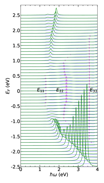
Let us firstly discuss the absorption spectra of doped SWNT for a particular . In Fig. 3 we plot of the SWNT as a function of photon energy for parallel and perpendicular polarization. Many spectra are plotted for different Fermi energies from to eV. For eV, since the first energy subband of conduction (valence) band is not occupied, we can observe interband transitions of all ’s with for the transitions between the valence and conduction bands. When we increase more than eV, the peaks start to disappear from to because the th subband in the conduction (valence) band begins to be occupied (unoccupied) for , and so on. The position of peaks (circles, triangles and diamonds for , and , respectively) is redshifted by increasing doping and then blueshifted before disappearing. The redshift of occurs because of the depolarization correction, which decreases with doping, whereas the blueshift attests the parabolic shape of the subbands. The depolarization correction can be seen as the inclusion of Coulomb interaction between electrons in the calculation of optical absorption [], since , where is the Coulomb potential and . Hence the dielectric function can be expressed as in Eq. (2). Without the inclusion of Coulomb interaction, the position of absorption peaks is constant by doping, not redshifted. Although we do not include the excitonic effect for simplicity, the presence of redshift in the peaks in our calculation is consistent with the previous work by Sasaki and Tokura Sasaki and Tokura (2018). It should be noted that, by the exclusion of excitonic effect, for nm, the deviation of the peak positions (defined as maxima of ) is still less than % in comparison with the exciton Kataura plot Jiang et al. (2007).
While the th subband is being occupied with electrons (or holes), the value of increases because the single-particle excitations occur only for the restricted -regions, which are far from Saito et al. (2000, 2005); Jiang et al. (2004), where the interband energy distance is larger. When the subband is partially occupied, a new peak for perpendicular polarization appears. We expect that such a peak is related with intersubband plasmon excitations for several reasons: (1) has a zero point close to the peak position, (2) the peak position is different from the single-particle intersubband transition, (3) the peak intensity strongly depends on Fermi energy and continuously increases even when the subbands are almost occupied and part of transitions is blocked, and (4) the blueshift with increasing the Fermi energy is opposite to the redshift for the single-particle excitation Igarashi et al. (2015). For highly positive doping eV, the second smaller peak is observed around eV as shown in Fig. 3. This peak is another type of plasmon, which differs from the first one at eV by the dominant contributions (see the more detailed discussion in Appendix B). Hereafter, we focus our attention to the first, main plasmon peak, since this one should easily be observed in experiments. The Fermi-energy dependent optical absorption shown in Fig. 3 is consistent with that previously discussed by Sasaki and Tokura Sasaki and Tokura (2018) for the armchair and zigzag SWNTs. However, the present result shows additional plasmon peaks (Appendix B) and different doping-type dependence (for and ), which appears by introducing more accurate energy band calculation.
III.2 Plasmon excitation in SWNT
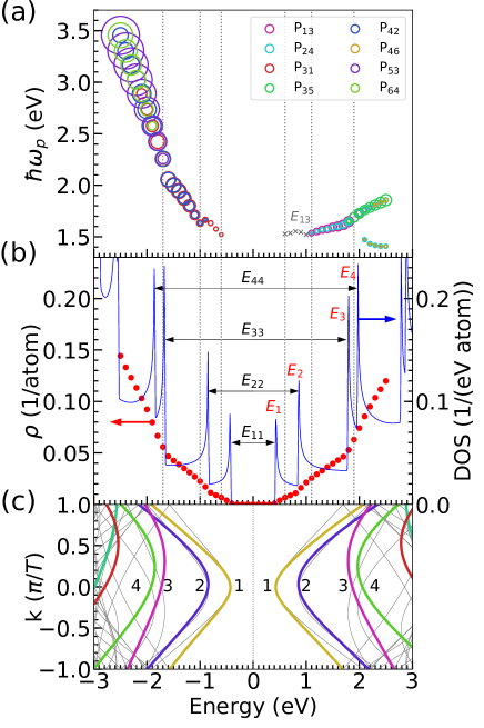
In Fig. 4(a) we plot the absorption peak position in the case of perpendicular polarization for the SWNT as a function of . The intensity of each peak is represented by the circle diameter. We attribute the peak as the plasmon peak and denote its frequency as when and is close ( meV) to . Each point in Fig. 4(a) consists of several circles which correspond to different contributions from the transition of the cutting line pair measured from the point. We denote the dominant contribution as Pij, where the threshold for dominant contribution was chosen as % of maximum contribution for each peak. Here we omit the valence and conduction band indices () since the dominant transition is the intersubband transition, . One can clearly observe the kink shape of the function, as well as the existence of the second plasmon branch at lower frequencies for eV (see Appendix B for details).
In Fig. 4(b) we display the density of states (DOS) and charge density as a function of Fermi energy for the nanotube. The charge density for electrons at is given by , where is the DOS. For holes at we modify the charge density formula by replacing the distribution function with . In Fig. 4(c) we show energy dispersion , where the energy subbands are labeled according to the approach discussed in Sec. II.2. The kink positions for the plasmon energy and the charge density are shown to be consistent to each other [see grey dotted lines in Fig. 4(b)]. In the three-dimensional (3D) Drude model, the plasmon frequency is known to be proportional to the square root of charge density ( ). For carbon nanotubes, the Fermi energy dependence was predicted to be consistent with 2D graphene result () de Abajo (2014). However, we see from Figs. 4(a) and 4(b) that the plasmon frequency is a function of , which in case of carbon nanotubes is the sum .
The kink in appears when passes through the next van Hove singularity () as shown in Fig. 4(b), which is followed by the Pauli blockade of the th subband and change in the dominant contribution to the plasmon from Pij to another P, where and for ( and for ). As seen from Fig. 4(a), the first dominant contribution is P13 (P31), the second dominant contribution after the first kink is P24 (P42), the third contribution after the second kink is P35 (P53) for (). The plasmon intensity [radius of circle in Fig. 4(a)] increases with increasing the Fermi energy and inceasing .
The asymmetry of plasmon peak intensity with respect to the -type and -type doping is consistent with asymmetric nature of for and . The minimum plasmon frequency as well as the Fermi energy at which the plasmon is excited basically depend on the energy band structure. For example, in Fig. 4(a), the asymmetry in the values of within valence and conduction bands influences the starting plasmon frequency ( eV for the valence band and eV for the conduction band). Meanwhile, the number of subbands under or above the Fermi level within the valence or conduction band is essential for accumulating negative contribution to dielectric function in order to observe . Therefore, the interplay between the intersubband transitions determines the asymmetric nature of the plasmon peak intensity in the -type and -type doping. Note that at eV both real and imaginary parts of are positive in the energy range of eV. In the case of p-doped (10,5) SWNT, the plasmon starts to appear at eV, after the 1st subband becomes partially unoccupied, in which the condition of is already satisfied. In the case of n-doping, the first small peak appears at eV. However, since , this peak is still not a plasmon, but is a single-particle intersubband transition . It is observed when the 1st subband is partially occupied and when the depolarization effect, which was completely suppressing absorption before, is relaxed. The true plasmon peak appears at eV, which corresponds to the 2nd subband partially occupied. Thus, the condition to observe the plasmon in SWNT for perpendicularly polarized light is to shift the Fermi level up higher than the bottom of the 2nd subband in conduction band Sasaki et al. (2016); Yanagi et al. (2018), or down lower than the top of the 1st subband in valence band.
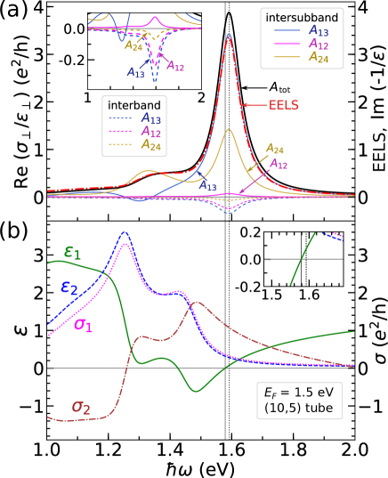
In Fig. 5(a), we plot intersubband and interband absorption spectra in case of perpendicular polarization for SWNT and eV. We define the absorption associated with the transition as , where is
| (6) |
For , when we consider the interband transitions, the th and the th subbands come from the valence and conduction band respectively. On the other hand, for the intersubband transitions, both subbands lie within the conduction band. The total absorption in Fig. 5(a) is contributed from all the interband and intersubband transitions. We see that the peak position and line shape of the absorption spectrum are consistent with those of EELS spectrum, which is given by .
As we already mentioned above, both optical conductivity and dielectric function are superpositions of contributions (, ) from different transitions between the subbands. To calculate absorption from the transition , we take only the corresponding term from the conductivity , while the dielectric function () is calculated for all pairs of interband and intersubband transitions according to Eq. (II.1). As an example, in the case of eV in Fig. 4(a) two main contributions are P13 and P24. In Fig. 5(a), we see the peak value of for intersubband absorption (solid lines) is one order-of-magnitude larger than that for interband absorption (dashed lines), which clearly shows that the plasmon has an intersubband nature. One may notice that the same P13 and P24 transitions are dominant for both intersubband and interband absorptions. However, the contributions have different signs and different order of magnitude.
Although the interband transitions seem to give negligible contribution to the plasmon intensity, they affect the redshift of the zero point for the dielectric function Sasaki and Tokura (2018), as shown in Fig. 5(b). In fact, the position of the maximum in absorption spectra (dotted vertical line) and the zero of (solid vertical line) are slightly different (by meV). This difference comes from , which decreases in the proximity of , as well as [Fig. 5(b)]. If the dielectric function is a real function of , the zero value would give the exact position of plasmon, which is not the case for a complex . Indeed, for and , the absorption and the energy loss-function have the following form:
| (7) | ||||
| (8) |
The maxima of and appear close to the , but not exactly at this point. The shift of the maxima strongly depends on slope of near the zero point of .
III.3 Mapping of intersubband plasmons
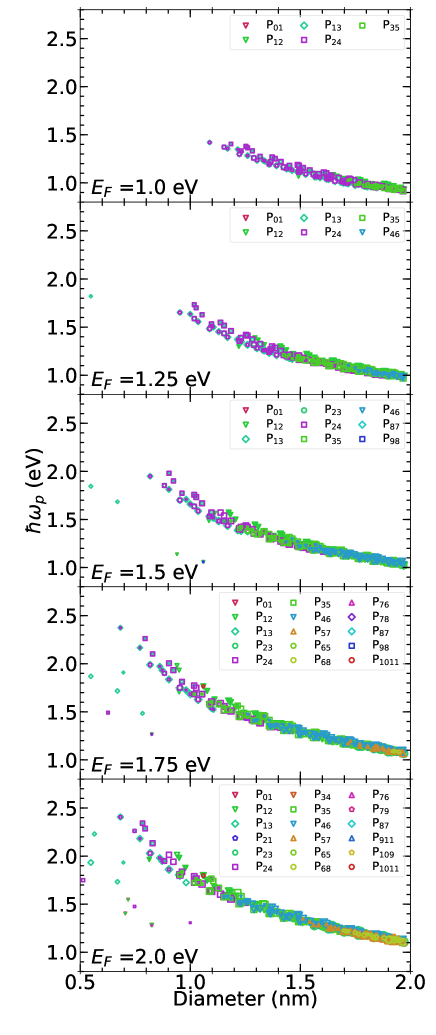
In Fig. 6, we plot energy of intersubband plasmon as a function of nanotube diameter , where nm, for five Fermi energies from to 2 eV. For eV plasmons are observed only in tubes with nm. With increasing , the number of tubes which have plasmonic excitations increases, since () is satisfied for a large even for smaller nanotubes. Plasmon energies , as well as their spreading for fixed and , are increasing with decreasing diameter. This indicates the presence of chirality dependence, which was neglected in the previous works Sasaki et al. (2016); Sasaki and Tokura (2018); de Abajo (2014). We see that the dominant contributions for smaller diameters and higher Fermi energies come from the cutting line pairs, which are close to the point. Therefore, the family spread due to the curvature effect is inherited by plasmon frequency. Hereafter, we focus on the Fermi energy and diameter dependence of plasmon frequency, since this information is useful for most experimental studies like the Kataura plot for optical absorption Sato et al. (2007); Nugraha et al. (2010) or Raman spectroscopy Sato et al. (2010). Chirality dependence of plasmon energy is a challenging point for the present method, since the band structure calculation by adopting the 3rd NNTB model is not satisfactory to build reliable chiral angle dependence or curvature effect Samsonidze et al. (2004).
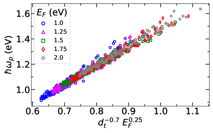
We numerically fit the diameter and the Fermi energy dependence with power law, as shown in Fig. 7. The result is:
| (9) |
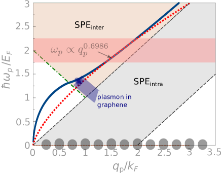
The (in nm) and (in eV) dependence in Fig. 7 can be understood from the dispersion of plasmon in graphene, which is shown in Fig. 8 Hwang and Sarma (2007). The intersubband plasmons in doped SWNTs, which are nothing but the azimuthal plasmons Sasaki et al. (2016), can be considered as the plasmons in the rolled graphene sheet, where we have the oscillations of charge around the nanotube axis. Rolling of graphene into SWNT results in the quantization of plasmon wave vector () following the reciprocal lattice vector Saito et al. (1998) in the SWNT since we consider the transitions of electron between different cutting lines. The magnitude of the reciprocal lattice vector is inversely proportional to the diameter, i.e., , similar to the wave vector of the electron along the circumferential direction . From Fig. 8, we can see that the dependence does not always hold for plasmon in graphene. The plasmon dispersion becomes almost linear to as it enters the interband single-particle excitation (SPE) regime Hwang and Sarma (2007). At the colored frequency range in Fig. 8 we fit the dispersion, where we get . Therefore, we expect for the plasmon frequency of SWNT, which confirms our finding in Eq. (9). It is noted that the of graphene’s plasmon is at relatively higher frequency range compared with the obtained plasmon frequency range for SWNTs as shown in Fig. 6. This is owing to the fact, that in SWNT the lower limit of photon energy for single particle excitation (the dash-dotted line in Fig. 8) would be smaller compared with the case of graphene due to the possible intersubband excitation of electron within the conduction band of SWNT. This lowering of energy limit for starting single particle excitation by intersubband transition (SPE) shifts the “almost” linear dispersion of plasmon in graphene to lower frequency range, too. Thus the fitting to “the almost linear dispersion” is justified.
The Fermi energy dependence of azimuthal plasmon in SWNT given by Eq. (9) can be also understood from the dispersion of plasmon in graphene shown in Fig. 8. Since the dispersion of plasmon in graphene is normalized to the Fermi energy as shown in Fig. 8, we can obtain the following equation:
| (10) |
where we use linear energy band of graphene, . Since , we expect the Fermi energy dependence to be , which is not exact but close to the obtained power law in Eq. (9). The difference with the obtained power law comes from the fact that the electron energy bands of SWNTs are not exactly linear as in graphene. It is noted that if we have the dependence of plasmon frequency in graphene, using Eq. (10), we will have as expected in the Drude model Hwang and Sarma (2007); Sasaki et al. (2016); de Abajo (2014).
IV Conclusion
We have systematically studied intersubband plasmon excitations in doped SWNTs as a function of diameter and the Fermi energy. The intersubband plasmons are excited due to the absorption of light with linear polarization perpendicular to the nanotube axis. The calculated plasmon frequency scales with the SWNT diameter and the Fermi energy as , which is a direct consequence of collective intersubband excitations of electrons in the doped SWNTs, but not a result of intraband transitions described by the Drude model. We also show that more than one branch of intersubband plasmons occurs even in one nanotube chirality. Our mapping of intersubband plasmon frequency may serve as a guide for experimentalists to search intersubband plasmons in many different SWNTs.
Acknowledgements.
D. S. thanks Skolkovo Institute of Science and Technology for financially supporting a three-month visit to Tohoku University for working on most parts of this project. A.R.T.N. acknowledges the Interdepartmental Program for Multidimensional Materials Science Leaders in Tohoku University. M. S. U. and R. S. acknowledge JSPS KAKENHI Grant Nos. JP18J10199 and JP18H01810, respectively. A. G. N. acknowledges Russian Science Foundation (Project identifier: 17-19-01787).Appendix A Optical matrix elements
The Schrdinger equation for a SWNT is given by:
| (11) |
where is the real-space Hamiltonian, is the electron wave vector, and () denotes the conduction (valence) band. The wave function can be expanded by a linear combination of the Bloch functions as follows:
| (12) |
where is the coefficient for the state . The Bloch function is expressed by
| (13) |
where denotes the 2 atomic orbital, gives the position of the th unit cell (with and unit vectors of hexagonal unit cell Saito et al. (1998)), is the position of th atom (A or B) in the th unit cell, and is the number of unit cells. Substituting Eq. (12) into Eq. (11) we obtain:
| (14) |
One can rewrite Eq. (A) in a matrix form multiplying to Eq. (A):
| (15) |
where and are Hamiltonian and overlap matrices respectively, defined by:
| (16) | ||||
| (17) |
and
| (18) | ||||
| (19) |
are considered up to the third nearest neighbor sites. Thus we come to the generalized problem for eigenvectors and eigenvalues of the form:
| (20) |
where gives the energy of valence and conduction subbands for particular SWNT and vector gives the coefficients for the wave function represented by Eq. (12). Within the zone-folding approach Eq. (20) is solved for Hamiltonian of 2D graphene, while the wave vector is taken as quasi-1D BZ for SWNT given by Saito et al. (1998):
| (21) |
where is the length of translational vector , is the number of cutting lines and denotes one-dimensional reciprocal lattice vector Saito et al. (1998). We adopt the wave vector notation of Eq. (21) to the single electron wave function in carbon nanotube as bra-ket style as .
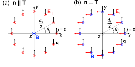
The single-particle Hamiltonian in the presence of external electromagnetic field is given by:
| (22) |
where is elemental charge and is the mass of electron. The optical matrix element is given by , where is Fourier component of the vector potential . For the light propagating parallel to the nanotube axis () [Fig. 9 (a)], in the th unit cell can be expressed as Sato et al. (2017)
| (23) |
In the case of perpendicularly polarized light () [Fig. 9(b)], is expressed as
| (24) |
where we take the direction of as and . We also take into account the fact that is sufficiently small compared with the unity, which means that in both cases the dominant contribution to matrix element comes from the first term, whereas the second term including can be neglected, which is known as the dipole approximation. Hereafter we will consider only the dominant terms. The optical matrix element in tight-binding approximation of Eq. (12) has the following form:
| (25) |
where is the bra-ket form for the atomic orbital introduced in Eq. (13). Let us discuss Eq. (A) for the two cases of parallel and perpendicular polarization one by one.
A.1 Perpendicular polarization
When we put Eq. (A) to Eq. (A), we get:
| (26) |
Here we define two-dimensional unit vectors originated from carbon nanotube lattice vectors Sato et al. (2017):
| (27) |
Then vectors and can be expressed by and as follows:
| (28) |
Using Eq. (A.1) we simplify the phase in Eq. (A.1):
| (29) |
Taking the summation on in Eq. (A.1) we get and . Finally the optical matrix elment takes the following form:
| (30) |
A.2 Parallel polarization
Appendix B Different plasmon branches
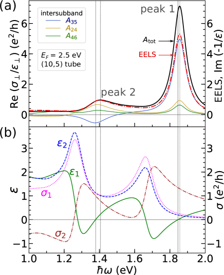
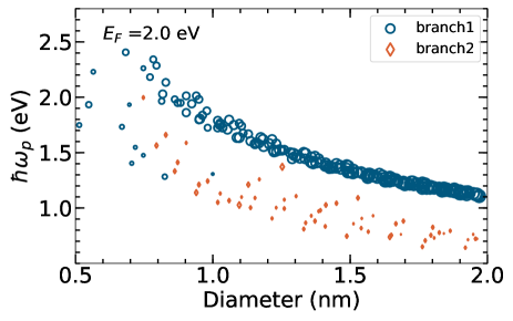
In Sec. III we discuss plasmon spectra only for major plasmons, which appear first and remain dominant in terms of its magnitude. However, for eV there exist another plasmon at the lower frequency as shown in Fig. 4 (a). Now in Fig. 10 (a) we plot the absorption spectra , as well as EELS spectra by (dash-dotted line), as a function of photon energy for the SWNT at eV. We can see two prominent peaks at eV (peak 1) and eV (peak 2), which differ by the dominant contributions [Fig. 4 (a)], i.e., P35 (from ) and P24 (from ), respectively . In particular, for the peak 2, the absorption , which is dominant for the peak 1, gives the negative contribution. This leads to a different behavior of the peak 2 as a function of .
In Fig. 10 (b), we plot , , , and as a function of photon energy. The condition on plasmon excitation is satisfied at two zero points of the real part of dielectric function (solid vertical line). The absorption maxima (dotted vertical line) are red-shifted regarding to , the shift is larger for peak 2, since is steeper around . Here we can clearly observe the effect of on plasmonic spectra: , where we denote and as the intensities of plasmon peaks 1 and 2. The presence of the second branch of intersubband plasmon have not been mentioned any of previous works of SWNTs. However in recent years, several ab initio studies show the similar second branch for bilayer graphene, nanoribbons, and other 2D materials Pisarra et al. (2016); Gomez et al. (2016); Torbatian and Asgari (2017, 2018). The intraband nature of the second branch plasmon in graphene nanoribbons was supposed by Gomez et al. Gomez et al. (2016), which is consistent with our results. We plot both plasmon branches for SWNT in Fig. 11 for different chiralities of SWNT with nm at eV. The lower plasmon peak P24 shows a larger chiral angle dependence since it comes from the cutting lines pairs closer to the point than the major plasmon P35. Thus the similar spreading character is observed for small-diameter SWNTs ( nm) and the second branch plasmon for bigger SWNTs ( nm).
References
- Kataura et al. (1999) H. Kataura, Y. Kumazawa, Y. Maniwa, I. Umezu, S. Suzuki, Y. Ohtsuka, and Y. Achiba, “Optical properties of single-wall carbon nanotubes,” Synth. Met. 103, 2555 (1999).
- Saito et al. (2000) R. Saito, G. Dresselhaus, and M. S. Dresselhaus, “Trigonal warping effect of carbon nanotubes,” Phys. Rev. B 61, 2981 (2000).
- Bachilo et al. (2002) S. M. Bachilo, M. S. Strano, C. Kittrell, R. H. Hauge, R. E. Smalley, and R. B. Weisman, “Structure-assigned optical spectra of single-walled carbon nanotubes,” Science 298, 2361 (2002).
- Weisman and Bachilo (2003) R. B. Weisman and S. M. Bachilo, “Dependence of optical transition energies on structure for single-walled carbon nanotubes in aqueous suspension: an empirical plot,” Nano Lett. 3, 1235 (2003).
- Avouris et al. (2006) Ph. Avouris, J. Chen, M. Freitag, V. Perebeinos, and J. C. Tsang, “Carbon nanotube optoelectronics,” Phys. Status Solidi B 243, 3197 (2006).
- Avouris et al. (2008) Ph. Avouris, M. Freitag, and V. Perebeinos, “Carbon-nanotube photonics and optoelectronics,” Nat. Photonics 2, 341 (2008).
- Kaskela et al. (2010) A. Kaskela, A. G. Nasibulin, M. Y. Timmermans, B. Aitchison, A. Papadimitratos, Y. Tian, Z. Zhu, H. Jiang, D. P. Brown, A. Zakhidov, and E. I. Kauppinen, “Aerosol-synthesized swcnt networks with tunable conductivity and transparency by a dry transfer technique,” Nano Lett. 10, 4349 (2010).
- Tsapenko et al. (2018) A. P. Tsapenko, A. E. Goldt, E. Shulga, Z. I. Popov, K. I. Maslakov, A. S. Anisimov, P. B. Sorokin, and A. G. Nasibulin, “Highly conductive and transparent films of -doped single-walled carbon nanotubes for flexible applications,” Carbon 130, 448 (2018).
- Ajiki and Ando (1994) H. Ajiki and T. Ando, “- effect in carbon nanotubes,” Phys. B 201, 349 (1994).
- Hwang et al. (2000) J. Hwang, H. H. Gommans, A. Ugawa, H. Tashiro, R. Haggenmueller, K. I. Winey, J. E. Fischer, D. B. Tanner, and A. G. Rinzler, “Polarized spectroscopy of aligned single-wall carbon nanotubes,” Phys. Rev. B 62, R13310 (2000).
- Jiang et al. (2004) J. Jiang, R. Saito, A. Grüneis, G. Dresselhaus, and M.S. Dresselhaus, “Optical absorption matrix elements in single-wall carbon nanotubes,” Carbon 42, 3169 (2004).
- Murakami et al. (2005) Y. Murakami, E. Einarsson, T. Edamura, and S. Maruyama, “Polarization dependence of the optical absorption of single-walled carbon nanotubes,” Phys. Rev. Lett. 94, 087402 (2005).
- Li et al. (2001) Z. M. Li, Z. K. Tang, H. J. Liu, N. Wang, C. T. Chan, R. Saito, S. Okada, G. D. Li, J. S. Chen, N. Nagasawa, and S. Tsuda, “Polarized absorption spectra of single-walled 4 carbon nanotubes aligned in channels of an – single crystal,” Phys. Rev. Lett. 87, 127401 (2001).
- Uryu and Ando (2006) S. Uryu and T. Ando, “Exciton absorption of perpendicularly polarized light in carbon nanotubes,” Phys. Rev. B 74, 155411 (2006).
- Spataru et al. (2004) C. D. Spataru, S. Ismail-Beigi, L. X. Benedict, and S. G. Louie, “Excitonic effects and optical spectra of single-walled carbon nanotubes,” Phys. Rev. Lett. 92, 077402 (2004).
- Wang (2005) F. Wang, “The optical resonances in carbon nanotubes arise from excitons,” Science 308, 838 (2005).
- Dukovic et al. (2005) G. Dukovic, F. Wang, D. Song, M. Y. Sfeir, T. F. Heinz, and L. E. Brus, “Structural dependence of excitonic optical transitions and band-gap energies in carbon nanotubes,” Nano Lett. 5, 2314 (2005).
- Jiang et al. (2007) J. Jiang, R. Saito, K. Sato, J. S. Park, Ge. G. Samsonidze, A. Jorio, G. Dresselhaus, and M. S. Dresselhaus, “Exciton-photon, exciton-phonon matrix elements, and resonant raman intensity of single-wall carbon nanotubes,” Phys. Rev. B 75, 035405 (2007).
- Sasaki et al. (2016) K. Sasaki, S. Murakami, and H. Yamamoto, “Theory of intraband plasmons in doped carbon nanotubes: Rolled surface-plasmons of graphene,” Appl. Phys. Lett. 108, 163109 (2016).
- Sasaki and Tokura (2018) K. Sasaki and Y. Tokura, “Theory of a carbon-nanotube polarization switch,” Phys. Rev. Applied 9, 034018 (2018).
- Yanagi et al. (2018) K. Yanagi, R. Okada, Y. Ichinose, Y. Yomogida, F. Katsutani, W. Gao, and J. Kono, “Intersubband plasmons in the quantum limit in gated and aligned carbon nanotubes,” Nat. Commun. 9, 1121 (2018).
- Senga et al. (2016) R. Senga, T. Pichler, and K. Suenaga, “Electron spectroscopy of single quantum objects to directly correlate the local structure to their electronic transport and optical properties,” Nano Lett. 16, 3661 (2016).
- Senga et al. (2018) R. Senga, T. Pichler, Y. Yomogida, T. Tanaka, H. Kataura, and K. Suenaga, “Direct proof of a defect-modulated gap transition in semiconducting nanotubes,” Nano Lett. 18, 3920 (2018).
- Kuzuo et al. (1992) R. Kuzuo, M. Terauchi, and M. Tanaka, “Electron energy-loss spectra of carbon nanotubes,” Jpn. J. Appl. Phys. 31, L1484 (1992).
- Kuzuo et al. (1994) R. Kuzuo, M. Terauchi, M. Tanaka, and Y. Saito, “Electron energy-loss spectra of single-shell carbon nanotubes,” Jpn. J. Appl. Phys. 33, L1316 (1994).
- Papagno and Caputi (1983) L. Papagno and L. S. Caputi, “Electronic structure of graphite: Single particle and collective excitations studied by , and edge loss techniques,” Surf. Sci. 125, 530 (1983).
- Liou et al. (2014) S. C. Liou, R. Breitwieser, C. H. Chen, W. W. Pai, G. Y. Guo, and M. W. Chu, “-plasmon dispersion in free-standing monolayer graphene investigated by momentum-resolved electron energy-loss spectroscopy,” Microsc. Microanal. 20, 1788 (2014).
- Hu et al. (2014) J. Hu, H. Zeng, C. Wang, Z. Li, C. Kan, and Y. Liu, “Interband plasmon of graphene: strong small-size and field-enhancement effects,” Phys. Chem. Chem. Phys. 16, 23483 (2014).
- Lin and Shung (1994) M. F. Lin and K. W.-K. Shung, “Plasmons and optical properties of carbon nanotubes,” Phys. Rev. B 50, 17744 (1994).
- Lin et al. (1996) M. F. Lin, D. S. Chuu, C. S. Huang, Y. K. Lin, and K. W.-K. Shung, “Collective excitations in a single-layer carbon nanotube,” Phys. Rev. B 53, 15493 (1996).
- de Abajo (2014) F. J. García de Abajo, “Graphene plasmonics: Challenges and opportunities,” ACS Photonics 1, 135 (2014).
- Bondarev (2012) I. V. Bondarev, “Single-wall carbon nanotubes as coherent plasmon generators,” Phys. Rev. B 85, 035448 (2012).
- Saito et al. (1998) R. Saito, G. Dresselhaus, and M. S. Dresselhaus, Physical properties of carbon nanotubes (Imperial College Press, London, 1998).
- Helm (2000) M. Helm, “The basic physics of intersubband transitions,” in Intersubband Transitions in Quantum Wells: Physics and Device Applications I, Semiconductors and Semimetals, Vol. 62, edited by H. C. Liu and F. Cappaso (Academic Press, 2000) pp. 1–99.
- Ajiki and Ando (1993) H. Ajiki and T. Ando, “Electronic states of carbon nanotubes,” J. Phys. Soc. Jpn. 62, 1255 (1993).
- Nakanishi and Ando (2009) T. Nakanishi and T. Ando, “Optical response of finite-length carbon nanotubes,” J. Phys. Soc. Jpn. 78, 114708 (2009).
- Ritchie (1957) R. H. Ritchie, “Plasma losses by fast electrons in thin films,” Phys. Rev. 106, 874 (1957).
- Raether (1980) H. Raether, Excitation of Plasmons and Interband Transitions by Electrons (Springer-Verlag, Berlin Heidelberg, 1980).
- Igarashi et al. (2015) T. Igarashi, H. Kawai, K. Yanagi, N. T. Cuong, S. Okada, and T. Pichler, “Tuning localized transverse surface plasmon resonance in electricity-selected single-wall carbon nanotubes by electrochemical doping,” Phys. Rev. Lett. 114, 176807 (2015).
- Ehrenreich and Cohen (1959) H. Ehrenreich and M. H. Cohen, “Self-consistent field approach to the many-electron problem,” Phys. Rev. 115, 786 (1959).
- Saito et al. (2004) R. Saito, A. Grüneis, Ge. G. Samsonidze, G. Dresselhaus, M. S. Dresselhaus, A. Jorio, L. G. Cançado, M. A. Pimenta, and A. G. Souza Filho, “Optical absorption of graphite and single-wall carbon nanotubes,” Appl. Phys. Lett. 78, 1099 (2004).
- Hertel and Moos (2000) T. Hertel and G. Moos, “Influence of excited electron lifetimes on the electronic structure of carbon nanotubes,” Chem. Phys. Lett. 320, 359 (2000).
- Reich et al. (2002) S. Reich, J. Maultzsch, C. Thomsen, and P. Ordejón, “Tight-binding description of graphene,” Phys. Rev. B 66, 035412 (2002).
- Chegel (2015) R. Chegel, “Third-nearest-neighbors tight-binding description of optical response of carbon nanotubes: Effects of chirality and diameter,” J. Electron. Mater. 44, 3500 (2015).
- Popov (2004) V. N. Popov, “Curvature effects on the structural, electronic and optical properties of isolated single-walled carbon nanotubes within a symmetry-adapted non-orthogonal tight-binding model,” New J. Phys. 6, 17 (2004).
- Samsonidze et al. (2003) Ge. G. Samsonidze, R. Saito, A Jorio, M. A. Pimenta, A. G. Souza Filho, A. Grüneis, G. Dresselhaus, and M. S. Dresselhaus, “The concept of cutting lines in carbon nanotube science,” J. Nanosci. Nanotechnol. 3, 431 (2003).
- Saito et al. (2005) R. Saito, K. Sato, Y. Oyama, J. Jiang, Ge. G. Samsonidze, G. Dresselhaus, and M. S. Dresselhaus, “Cutting lines near the fermi energy of single-wall carbon nanotubes,” Phys. Rev. B 72, 153413 (2005).
- (48) The plasmon data sets are open at http://github.com/DariaSatco/PlasmonOutput, while the absorption code is available at https://github.com/DariaSatco/cntabsorpt.
- Sato et al. (2007) K. Sato, R. Saito, J. Jiang, G. Dresselhaus, and M. S. Dresselhaus, “Discontinuity in the family pattern of single-wall carbon nanotubes,” Phys. Rev. B 76, 195446 (2007).
- Nugraha et al. (2010) A. R. T. Nugraha, R. Saito, K. Sato, P. T. Araujo, A. Jorio, and M. S. Dresselhaus, “Dielectric constant model for environmental effects on the exciton energies of single wall carbon nanotubes,” Appl. Phys. Lett. 97, 091905 (2010).
- Sato et al. (2010) K. Sato, R. Saito, A.R.T. Nugraha, and S. Maruyama, “Excitonic effects on radial breathing mode intensity of single wall carbon nanotubes,” Chem. Phys. Lett. 497, 94 (2010).
- Samsonidze et al. (2004) Ge. G. Samsonidze, R. Saito, N. Kobayashi, A. Grüneis, J. Jiang, A. Jorio, S. G. Chou, G. Dresselhaus, and M. S. Dresselhaus, “Family behavior of the optical transition energies in single-wall carbon nanotubes of smaller diameters,” Appl. Phys. Lett. 85, 5703 (2004).
- Hwang and Sarma (2007) E. H. Hwang and S. D. Sarma, “Dielectric function, screening, and plasmons in two-dimensional graphene,” Phys. Rev. B 75, 205418 (2007).
- Sato et al. (2017) N. Sato, Y. Tatsumi, and R. Saito, “Circular dichroism of single-wall carbon nanotubes,” Phys. Rev. B 95, 155436 (2017).
- Pisarra et al. (2016) M. Pisarra, A. Sindona, M. Gravina, V. M. Silkin, and J. M. Pitarke, “Dielectric screening and plasmon resonances in bilayer graphene,” Phys. Rev. B 93, 035440 (2016).
- Gomez et al. (2016) C. Vacacela Gomez, M. Pisarra, M. Gravina, J. M. Pitarke, and A. Sindona, “Plasmon modes of graphene nanoribbons with periodic planar arrangements,” Phys. Rev. Lett. 117, 116801 (2016).
- Torbatian and Asgari (2017) Z. Torbatian and R. Asgari, “Plasmon modes of bilayer molybdenum disulfide: a density functional study,” J. Phys. Condens. Matter 29, 465701 (2017).
- Torbatian and Asgari (2018) Z. Torbatian and R. Asgari, “Plasmonic physics of crystalline materials,” Appl. Sci. 8, 238 (2018).