Nanomechanical single-photon routing
Abstract
The merger between integrated photonics and quantum optics promises new opportunities within photonic quantum technology with the very significant progress on excellent photon-emitter interfaces and advanced optical circuits. A key missing functionality is rapid circuitry reconfigurability that ultimately does not introduce loss or emitter decoherence, and operating at a speed matching the photon generation and quantum memory storage time of the on-chip quantum emitter. This ambitious goal requires entirely new active quantum-photonic devices by extending the traditional approaches to reconfigurability. Here, by merging nano-optomechanics and deterministic photon-emitter interfaces we demonstrate on-chip single-photon routing with low loss, small device footprint, and an intrinsic time response approaching the spin coherence time of solid-state quantum emitters. The device is an essential building block for constructing advanced quantum photonic architectures on-chip, towards, e.g., coherent multi-photon sources, deterministic photon-photon quantum gates, quantum repeater nodes, or scalable quantum networks.
Photonic quantum technologies offer unprecedented opportunities to implement quantum optics experiments directly on a chip, thereby replacing large-scale optical setups with integrated devices interfacing high-efficiency single-photon emitters, waveguide circuitry, and detectors obrien_photonic_2009 . Scaling up to multi-qubit systems is the key challenge, and to this end modern device nanofabrication is a major asset. While significant progress has been made on the fabrication of advanced quantum optical circuits for processing single photons politi_silica_2008 ; crespi_integrated_2013 ; wang_multidimensional_2018 it appears a daunting challenge to scale up quantum processors based alone on linear optics and single photons towards, e.g., quantum computing knill_scheme_2001 ; rudolph_why_2017 . It is therefore highly desirable to develop additional photonic quantum resources in order to break new grounds.
The development of a deterministic and coherent interface between a single photon and a single emitter, as recently demonstrated with atoms thompson_coupling_2013 ; reiserer_cavity_2015 , defect centers sipahigil_integrated_2016 , and quantum dots lodahl_interfacing_2015 , leads to novel opportunities for quantum photonics. It enables constructing multi-photon sources wang_high-efficiency_2018 , photon-photon quantum gates duan_scalable_2004 , nonlinear operations at the single-photon level chang_single-photon_2007 , and the generation of multi-photon entangled cluster states lindner_proposal_2009 . Applications areas include device-independent quantum key distribution mattar_device_2018 , all-photonic quantum repeaters azuma_allphotonic_2015 ; buterakos_deterministic_2017 , photonic quantum computing pichler_universal_2017 , and connecting distant and heterogeneous quantum nodes via a photonic network hensen_loophole_2015 . As a quantitative benchmark it has been estimated that photon coupling efficiencies beyond 90 % and local processing speeds faster than 100 ns are required in order to develop advantageous all-photonic quantum-repeater protocols muralidharan_optimal_2016 , which is challenging yet feasible with, e.g., quantum dots embedded in nanophotonic waveguides lodahl_quantum-dot_2017 . It is here essential to be able to reconfigure the circuit and route photonic qubits between different quantum nodes (see Fig. 1a) with very low loss and at a speed that is compatible with the emitter qubit coherence time, which for efficient solid-state emitters like quantum dots and defect centers typically is in the range of s - ms warburton_single_2013 ; sukachev_silicon_2017 . Such low loss, tunable, and fast photonic circuitry has not yet been implemented on devices containing active photon emitters and spins, and existing tuning mechanisms based on thermal heating and the electro-optic effect do not meet these demands: while the thermo optic effect is slow and not compatible with cryogenic operation, the electro-optic effect is material-dependent and typically results in a large device footprint with constraints for scaling and efficiency. Consequently, a fundamentally different approach is required.
In this work, we merge the two research disciplines of deterministic photon-emitter interfaces and nano-opto-electro-mechanics in order to bridge that gap. Electrically induced mechanical deformation of the waveguide circuit constitutes a novel and elegant approach to photon routing, which is independent of intrinsic material properties and therefore can be implemented for many material systems, wavelengths, and temperatures midolo_nano-opto-electro-mechanical_2018 , including for active photonic chips containing quantum emitters perahia_electrostatically_2010 ; midolo_spontaneous_2012 ; bishop_electro-mechanical_2018 . At the nanoscale, the opto-electro-mechanical interaction is much stronger than refractive-index tuning effects. Therefore, the device footprint, switching time, and insertion loss are significantly reduced, meaning that circuit complexity can be scaled up. As a quantitative prospect of the technology, we estimate that a single-qubit unitary gate composed of a controllable beam splitter and a phase shifter could be built with a footprint smaller than 30 m2 and with a response time of 100–200 ns. With such an approach, fully-integrated photonic quantum processing may be within reach.
Nanomechanical control of directional couplers
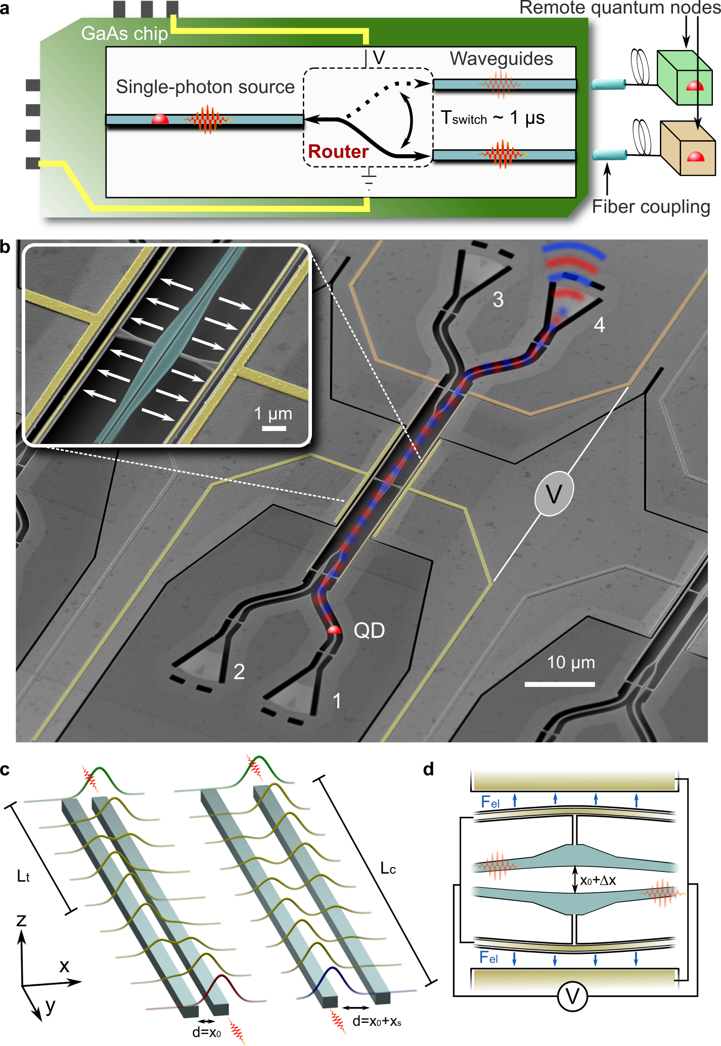
The integrated photon router has been fabricated in thin GaAs membranes with embedded InAs quantum dots, cf. the scanning electron micrograph (SEM) of Fig. 1b. It consists of suspended dielectric waveguides connected to capacitive nanomechanical actuators, whose role is to convert a voltage signal into the mechanical motion required for optical switching. The principle of operation is that of a gap-variable directional coupler with an adjustable coupling strength , where is the spatial decay of the fundamental transverse electric mode supported by each individual waveguide and is the waveguide separation. Figure 1c shows schematically the propagation of light in such a device when initially illuminated through one port only. If the waveguides are identical (phase matching condition), the optical power is fully transferred to the other waveguide after a transfer length . At the end of the coupling section (length ) the splitting ratio is
| (1) |
To tune the splitting ratio, can be changed using an external force to induce a -change in the argument of Eq. 1. The exponential dependence of on implies that it is advantageous to work at small separations (nano-slots) in order to increase the sensitivity of the splitting ratio to small deformations and to reduce the device footprint midolo_nano-opto-electro-mechanical_2018 . Full switching is only possible if light transfers at least once from one waveguide to the next i.e. , suggesting a device scaling law, which is directly proportional to the transfer length at rest, or , where is the initial gap between the waveguides. Reducing the gap to few tens of nm, which is realistic with current fabrication technology, would imply that a coupling length below 5 m could be achieved, showing the huge integration potential of nanomechanical switches. For further information about the theory of gap-variable directional couplers, see Supplementary Information.
The mechanical deformation is obtained by capacitive actuation, as shown schematically in Fig. 1d and visible in the SEM image of Fig. 1b. Each waveguide is connected via thin tethers to a pair of electrodes forming gap-variable capacitors whose distance at rest is 300 nm in the current device. When a bias voltage is applied across the electrodes, they bend and increase the waveguide separation by . This geometry allows us to double the displacement of a single actuator by electrically wiring both sides of the device in parallel. See Supplementary Information for details on the device design.
Single-photon routing
The device is characterized at cryogenic temperature (T = 10 K) in a Helium flow cryostat. The data of Fig. 2 show the ability to perform high-extinction routing of single photons emitted from single quantum dots (QDs) in the device. Figure 2a shows an emission spectrum when optically exciting multiple QD emission lines that can be spectrally selected. By displacing the waveguides with voltage, the emitted photons from each QD are distributed to the two output ports as indicated in the inset. Unlike thermo-optic methods elshaari_-chip_2017 , the mechanical motion is decoupled from the QD, which is confirmed by the absence of de-tuning of the excitonic emission. Consequently, the device enables disturbance-free routing of single photons from the embedded QDs.
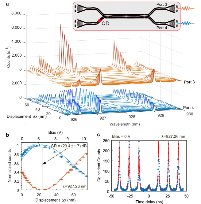
We focus on the QD located at a wavelength of 927.26 nm. The integrated counts as a function of displacement are plotted in Fig. 2b and normalized according to the coupling efficiency (see Supplementary Information for details). The applied voltage is stepped over the 0 - 10.2 V range multiple times to test the reproducibility of the switching curve, resulting in the small deviations of the integrated counts indicated by the error bars. A maximum extinction ratio of (-23.4 1.7) dB is measured at a displacement of 24 nm (i.e. at a bias voltage of 7 V) corresponding to a splitting ratio of %. The solid lines show the theoretical model, cf. Supplementary Information, used to calibrate the displacement in the transmission measurements. A very good agreement with the model of a loss-less and perfectly balanced router is observed whereas minor deviations are attributed to a small residual reflectivity from the gratings. These data show that QD emission can be routed on-chip with exceedingly high extinction. Notably the demonstrated performance is on par with the extinction values previously demonstrated on single Mach-Zehnder interferometers with thermo-optic phase shifters (i.e. in the 20–30 dB range). It could even be further improved by adopting a double-gate approach of cascading a second tunable routing circuit to direct any residual unwanted signal to a third idle output port suzuki_ultra_2015 . High-extinction single-photon routing on the same chip as the emitter is key in order to construct deterministic quantum gates for photons.
To confirm the single-photon nature of the routing, we perform a pulsed Hanbury-Brown and Twiss experiment. A bandpass filter (0.3 nm bandwidth) is used to select only one emission line from the QD spectrum. The measured second-order auto-correlation function, , is shown in Fig. 2c at a power ( W is the saturation power of the QD) and the peaks are modelled with exponential functions. The recorded single-photon purity is limited by the density of QDs and the applied above-band excitation scheme, and could readily be improved further kirsanske_indistinguishable_2017 . The low insertion loss of the device is confirmed by recording the total photon count rate from the device. No evidence of increased loss from the photon router was observed, since the recorded count rate on the present device was comparable to similar devices without the presence of an active routing section. From these measurements an insertion loss below dB/switch is obtained. Note also that the device comprises engineered gratings for highly efficient (60 %) coupling from the chip to an optical fiber zhou_high_2018 . See Supplementary Information for further details on the analysis of the device efficiency.
The demonstrated performance of the single-photon router directly open new opportunities for quantum photonics. As a concrete example, a de-multiplexed source of single photons can be constructed by using a single deterministically coupled emitter combined with low-loss and high-contrast routing. By cascading the nanomechanical routers, a 10-photon source can be achieved, which is significantly beyond current state-of-the-art of using bulk electro-optical modulators wang_high-efficiency_2018 . With the use of QDs at telecom wavelengths ward_on-demand_2005 and further realistic improvements of the device, the technology could be scaled up to . For comparison certain quantum algorithms, such as boson sampling, are expected to show quantum advantage for wu_benchmark_2018 . The detailed estimates of the achievable multi-photon generation rates are presented in the Supplementary Information. It should be emphasized that these advantageous resource estimates are performed for the specific case of emitting independent photons, while adding, e.g., the spin quantum memory could lead to even more efficient generation of non-trivial photonic quantum resources.
Time response
Micro-electro-mechanical and thermo-optic switches are known for their slow response, i.e. in the kHz range. A nanomechanical router, on the other hand, allows pushing this boundary further, entering the MHz regime. Such fast switching is required in quantum-information protocols exploiting solid-state quantum memories, such as a single spin in a QD warburton_single_2013 . The time response of the nanomechanical single-photon router is determined by the mechanical susceptibility of the actuator, i.e. by its mechanical quality factor and its fundamental resonant frequency , which sets an upper limit to the switching rate. Figure 3a shows the calculated in-plane mechanical resonant mode. For a perfectly symmetric structure, two fundamental and degenerate in-plane resonances are found numerically, with MHz. The mechanical quality factor at cryogenic temperatures and in vacuum is mainly determined by the clamping losses, which for suspended bridge geometries at these scales gives – wilson_intrinsic_2008 . Details on the mechanical spectrum and its measurement are given in Supplementary Information.
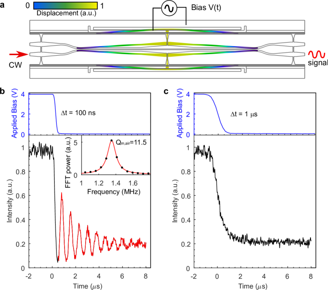
Ideally, a critically damped (i.e. ) resonator can respond to step signals within a time as short as ns without oscillations. In this mode of operation, it is therefore desirable to increase the damping, which in the experiment can be done by operating the device at atmospheric pressure. Critical damping at cryogenic conditions can be achieved, e.g., by introducing an inert buffer gas into the cryostat. A continuous-wave laser is directed to one input port of the device while a step voltage drives the actuator (see Fig. 3a). The applied bias of 4 V is sufficiently low to ensure that the laser intensity at the output is only weakly modulated and therefore proportional to the waveguide displacement, allowing us to probe the mechanical motion optically. The intensity-modulated laser output is collected into a fiber connected to a fast avalanche photodiode, whose electrical signal is measured on an oscilloscope. Ring-down measurements have been performed with a variable ramp-down time to investigate the time scales involved in the mechanical response. The time traces of the photodiode signal (and applied bias) are shown in Fig. 3b and 3c, for ns and 1 s, respectively.
Figure 3a illustrates the case when the force on the actuator is suddenly released over a time much shorter than the natural period of the device, i.e. when . Therefore, the input signal excites the fundamental mechanical resonance of the waveguides and the device responds with damped oscillations. The inset of Fig. 3b shows the Fourier transform of the damped signal (highlighted in red), revealing a single mechanical resonance at MHz (in accordance with numerical calculations) and with . This mode of operation is useful to identify the mechanical resonances of the device but does not correspond to a situation where the device is rapidly and deterministically reconfigured. Indeed, the time required for the mechanical oscillations to stabilize is approximately s. For certain applications resonant driving of the device may be favorable, e.g., in synchronized switching of photons in de-multiplexing setup aimed at transforming one deterministic single-photon source into multiple sources lodahl_quantum-dot_2017 . In this case, boosting the quality factor to higher values by, e.g., suppressing clamping losses, could be advantageous to achieve ultra-low switching voltages in the millivolt regime. Additional data on resonant driving are presented in Supplementary Information.
When (see Fig. 3c), the mechanical response follows the dynamics of the input signal and stabilizes within approximately 1 s. It is found that the device can be driven without exciting any mechanical resonances of the device, i.e. this is the mode of operation of reconfigurable photon routing which is demonstrated on the microsecond time-scale. This would be useful for programming arbitrary sequences of qubit rotations or quickly routing single-photons into various channels, as illustrated schematically in Fig. 1a. We emphasize that the resonant frequency scales with the device length according to , hence the response time could be significantly reduced to s by designing shorter coupling lengths. These time-scales of deterministic on-chip single-photon routing offer new opportunities for high-speed quantum communication.
Conclusion
We have demonstrated an on-chip reconfigurable circuit, which was used for routing single photons emitted from QDs. The small footprint and the planar design allow cascading multiple devices in a single chip, enabling more complex routing schemes. The concept could be readily transferred to other material platforms containing high-quality solid-state emitters such as vacancy centers in diamond as well as to other wavelengths. A path towards making even smaller and faster devices, is to further reduce the waveguide separation midolo_nano-opto-electro-mechanical_2018 . This could be achieved by, for example, reversing the direction of actuation or by fabricating smaller waveguide slots. The seamless integration with QDs makes the presented device an ideal platform for source-integrated re-configurable quantum photonic circuits. It allows the integration of hybrid systems involving quantum emitters, electrical devices, and mechanical resonators, which have recently drawn much attention for precision sensing treutlein_hybrid_2014 . A scalable re-configurable single-photon router is the cornerstone of protocols for de-multiplexing single-photon sources lenzini_active_2016 , boson sampling, and linear optical quantum computing. Furthermore, this device could be combined with mechanically tunable phase shifters poot_broadband_2014 , in providing a path to programmable nanomechanical unitary gates. Together with deterministic positioning of QDs, efficient out-coupling schemes, and detectors this approach will enable advanced quantum-information processing applications with single photons beyond the linear-optics quantum computing paradigm that has been inspirational to integrated quantum photonics research.
Acknowledgements
We acknowledge T. Pregnolato for assistance in fabrication, S. L. Hansen, R. Uppu, and A. Fiore for useful discussions. We gratefully acknowledge financial support from the Danish National Research Foundation (Center of Excellence ’Hy-Q’), the European Research Council (ERC Advanced Grant ’SCALE’), Innovation Fund Denmark (Quantum Innovation Center ’Qubiz’), the Villum Foundation, the Danish Research Infrastructure Grant (QUANTECH), and the Danish Council for Independent Research (grant number 4184-00203). A.L., R.S., and A.D.W. gratefully acknowledge support of BMBF (Q.Link.X 16KIS0867) and the DFG (TRR 160).
References
- (1) O’Brien, J. L., Furusawa, A. & Vučković, J. Photonic quantum technologies. Nat. Photon. 3, 687–695 (2009).
- (2) Politi, A., Cryan, M. J., Rarity, J. G., Yu, S. & O’Brien, J. L. Silica-on-silicon waveguide quantum circuits. Science 320, 646–649 (2008).
- (3) Crespi, A. et al. Integrated multimode interferometers with arbitrary designs for photonic boson sampling. Nat. Photon. 7, 545–549 (2013).
- (4) Wang, J. et al. Multidimensional quantum entanglement with large-scale integrated optics. Science 360, 285–291 (2018).
- (5) Knill, E., Laflamme, R. & Milburn, G. J. A scheme for efficient quantum computation with linear optics. Nature 409, 46–52 (2001).
- (6) Rudolph, T. Why I am optimistic about the silicon-photonic route to quantum computing. APL Photon. 2, 030901 (2017).
- (7) Thompson, J. D. et al. Coupling a single trapped atom to a nanoscale optical cavity. Science 340 1202–1205 (2013).
- (8) Reiserer, A. & Rempe, G. Cavity-based quantum networks with single atoms and optical photons. Rev. Mod. Phys. 87, 1379–1418 (2015).
- (9) Sipahigil, A. et al. An integrated diamond nanophotonics platform for quantum-optical networks. Science 354, 847–850 (2016).
- (10) Lodahl, P., Mahmoodian, S. & Stobbe, S. Interfacing single photons and single quantum dots with photonic nanostructures. Rev. Mod. Phys. 87, 347–400 (2015).
- (11) Wang, H. et al. High-efficiency multiphoton boson sampling. Nat. Photonics 11 361–365 (2017).
- (12) Duan, L. M. & Kimble, H. J. Scalable photonic quantum computation through cavity-assisted interactions. Phys. Rev. Lett. 92, 127902 (2004).
- (13) Chang, D. E., Sørensen, A. S., Demler, E. A. & Lukin, M. D. A single-photon transistor using nanoscale surface plasmons. Nat. Phys. 3, 807–8012 (2007).
- (14) Lindner, N. H. & Rudolph, T. Proposal for pulsed on-demand sources of photonic cluster state strings. Phys. Rev. Lett. 103, 113602 (2009).
- (15) Máttar, A. et al. Device-independent quantum key distribution with single-photon sources. https://arxiv.org/abs/1803.07089 (2018).
- (16) Azuma, K., Tamaki, K. & Lo, H.-K. All-photonic quantum repeaters. Nat. Comm. 6, 6787 (2015).
- (17) Buterakos, D., Barnes, E. & Economou, S. E. Deterministic generation of all-photonic quantum repeaters from solid-state emitters. Phys. Rev. X 7, 041023 (2017).
- (18) Pichler, H., Choi, S., Zoller, P. & Lukin, M. D. Universal photonic quantum computation via time-delayed feedback. Proc. Natl Acad. Sci. USA 114, 11362–11367 (2017).
- (19) Hensen, B. et al. Loophole-free bell inequality violation using electron spins separated by 1.3 kilometres. Nature 526, 682–686 (2015).
- (20) Muralidharan, S. et al. Optimal architectures for long distance quantum communication. Sci. Rep. 6, 20436 (2016).
- (21) Lodahl, P. Quantum-dot based photonic quantum networks. Quantum Sci. Technol. 3, 013001 (2018).
- (22) Warburton, R. J. Single spins in self-assembled quantum dots. Nat. Mater. 12, 483–493 (2013).
- (23) Sukachev, D. D. et al. Silicon-vacancy spin qubit in diamond: a quantum memory exceeding 10 ms with single-shot state readout. Phys. Rev. Lett. 119, 223602 (2017).
- (24) Midolo, L., Schliesser, A. & Fiore, A. Nano-opto-electro-mechanical systems Nat. Nanotechnol. 13, 11–18 (2018).
- (25) Perahia, R., Cohen, J. D., Meenehan, S., Mayer Alegre, T. P. & Painter, O. Electrostatically tunable optomechanical “zipper” cavity laser. Appl. Phys. Lett. 97, 191112 (2010).
- (26) Midolo, L. et al. Spontaneous emission control of single quantum dots by electromechanical tuning of a photonic crystal cavity. Appl. Phys. Lett. 101, 091106 (2012).
- (27) Bishop, Z. K. et al. Electro-mechanical control of an on-chip optical beam splitter containing an embedded quantum emitter, Opt. Lett. 43, 2142–2145 (2018).
- (28) Elshaari, A. W. et al. On-chip single photon filtering and multiplexing in hybrid quantum photonic circuits. Nat. Commun. 8, 379 (2017).
- (29) Suzuki, K. et al. Ultra-high-extinction-ratio 2 2 silicon optical switch with variable splitter. Opt. Express 23, 9086–9092 (2015).
- (30) Kiršanskė, G. et al. Indistinguishable and efficient single photons from a quantum dot in a planar nanobeam waveguide. Phys. Rev. B 96, 165306 (2017).
- (31) Zhou, X. et al. High-efficiency shallow-etched grating on GaAs membrane for quantum photonic applications. https://arxiv.org/abs/1809.03189 (2018).
- (32) Ward, M. B. et al. On-demand single-photon source for 1.3 m telecom fiber. Appl. Phys. Lett. 86, 201111 (2005).
- (33) Wu, J. et al. A benchmark test of boson sampling on Tianhe-2 supercomputer. Natl. Sci. Rev. 5, 715–720 (2018).
- (34) Wilson-Rae, I. Intrinsic dissipation in nanomechanical resonators due to phonon tunneling. Phys. Rev. B 77, 245418 (2008).
- (35) Treutlein, P., Genes, C., Hammerer, K., Poggio, M. & Rabl, R. Hybrid Mechanical Systems (Springer Berling Heidelberg, 2014).
- (36) Lenzini, F. et al. Active demultiplexing of single photons from a solid-state source. Laser Photonics Rev. 11, 1600297 (2017).
- (37) Poot, M. & Tang, H. X. Broadband nanoelectromechanical phase shifting of light on a chip. Appl. Phys. Lett. 104, 061101 (2014).