Enhanced Rashba spin-orbit coupling in core-shell nanowires by the interfacial effect
Abstract
We report on calculations of Rashba spin-orbit coupling controlled by external gates in InAs/InAsP core-shell nanowires. We show that charge spilling in the barrier material allows for a stronger symmetry breaking than in homoegenous nano-materials, inducing a specific interface-related contribution to spin-orbit coupling. Our results qualitatively agree with recent experiments [S. Futhemeier et al., Nat. Commun. 7, 12413 (2016)] and suggest additional wavefunction engineering strategies to enhance and control spin-orbit coupling.
Understanding and controlling spin-orbit coupling (SOC) is critical in semiconductor physics. In particular, in semiconductor nanowires (NWs) Kokurin (2015, 2014); Kammermeier et al. (2016); Winkler et al. (2017); Wójcik, Bertoni, and Goldoni (2018a); Campos et al. (2018); Luo, Li, and Zunger (2017) SOC is essential for to the development of a suitable hardware for topological quantum computation Alicea (2010); Sau (2017), with qubits encoded in zero-mode Majorana states which are supported by hybrid semiconductor-superconductor NWs Kitaev (2003); Sau, Tewari, and Das Sarma (2012); Mourik et al. (2012); Mastomäki et al. (2017); Albrecht et al. (2016); Manolescu et al. (2017). Among other parameters, qubit protection at sufficiently high temperatures relies on a large SOC which determines the topological gap. Additionally, electrical control of SOC is necessary in the realization of spintronic devices Fabian et al. (2007); Datta and Das (1990); Schliemann, Egues, and Loss (2003); Wójcik and Adamowski (2016); Wójcik et al. (2014); Wójcik and Adamowski (2017); Das et al. (2012); Debray, Rahman, and Muhammad (2009); Kohda et al. (2012); Rossella et al. (2014); Iorio et al. (2018).
SOC arises from the absence of inversion symmetry of the electrostatic potential. In semiconductor NWs, typically having a prismatic shape, finite SOC may be induced by distorting the quantum confinement (Rashba SOC Rashba (1960)) by means of external gates, with the advantage of electrical control. A lattice contribution (Dresselhaus SOC Dresselhaus (1955)) is typically small and may vanish in specific crystallographic directions - for zincblende NWs, the Dresselhaus term vanishes along [111] due to the inversion symmetry.
The Rashba SOC constant has been investigated experimentally in homogeneous NWs based on the strong SOC materials InSb van Weperen et al. (2015); Kammhuber et al. (2017) and InAs Scherübl et al. (2016); Hansen et al. (2005); Dhara et al. (2009); Roulleau et al. (2010); Estévez Hernández et al. (2010). Recently Wójcik, Bertoni, and Goldoni (2018a), we reported on a approach applied to homogeneous NWs which predicts from compositional and structural parameters only. Our calculations performed for InSb NWs Wójcik, Bertoni, and Goldoni (2018a) and InAs NWs Wójcik, Bertoni, and Goldoni (2018b) generally confirm recent experiments in homogeneous NWs van Weperen et al. (2015); Scherübl et al. (2016), exposing values of exceeding by one order of magnitude those reported for 2D analogous planar systems Kallaher et al. (2010a, b); Herling et al. (2017). Moreover, proved to be strongly tunable with external gates in samples and configurations which can be routinely realized with current technology.
For a quantitative prediction of SOC, it is necessary to take into account valence-to-conduction band coupling, the explicit geometry and crystal structure of the NW, and the electron gas distribution which, in turn, must be self-consistently determined by quantum confinement effects, interaction with dopants and electron-electron interaction. Indeed, in NWs the electron gas localization, and ensuing SOC, is a non-trivial result of competing energy contributions. As a function of doping concentration and ensuing free charge density, the electron gas evolves from a broad cylindrical distribution in the NW core (low density regime) to coupled quasi-1D and quasi-2D channels at the NW edges (large density regime) Bertoni et al. (2011); Funk et al. (2013); Jadczak et al. (2014); Royo, Bertoni, and Goldoni (2014). Until polygonal symmetry holds, regardless. However, external gates easily remove the symmetry; again, how moves from zero under the influence of the external gates strongly depends on the charge density regime Wójcik, Bertoni, and Goldoni (2018a).
In this Letter we extend and apply the approach to core-shell NWs (CSNWs) and expose a novel mechanism through which SOC can be further tailored, and possibly enhanced. Epitaxially overgrown shells are often used in NW technology, either as a passivating layer improving optical performance Jabeen et al. (2008), or as a technique to engineer radial heterostructures Spirkoska et al. (2009). Here we show that CSNWs allow for an increased flexibility in distorting the electron gas of the NWs, giving rise to a specific, interfacial SOC contribution Devizorova and Volkov (2013); Ivchenko, Kaminski, and Rössler (1996) which substantially increases the total SOC. We make the case for InAs/InAsP CSNWs, a systems of specific interest in photonics Treu et al. (2013) and electrical engineering Liu et al. (2013). Our results qualitatively agree with the recent experiments by Furthmeier et al. in Ref. Furthmeier et al., 2016, where the enhancement of SO coupling was measured in GaAs/AlGaAs CSNW, and establish a strategy to increase the SOC in Majorana InAs NWs.
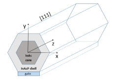
We consider CSNWs with hexagonal cross-section Sitek et al. (2018) grown along [111] (see Fig. 1), assuming in-wire translational invariance along . The used approach is described in full in Ref. Wójcik, Bertoni, and Goldoni, 2018a; here we focus on generalizations required to account for the contribution of the internal heterointerface. The Kane Hamiltonian is given by Fabian et al. (2007)
| (1) |
where and are the diagonal matrices corresponding to the conduction () and valence (, ) bands whose expressions are given in Ref. Wójcik, Bertoni, and Goldoni, 2018a. Using the perturbative transformation , the Hamiltonian (1) reduces to a effective Hamiltonian for the conduction band electrons. Emphasizing the dependence of material parameters on the position, ,
| (2) |
where are the Pauli matrices and is the effective mass given by
| (3) |
where is the conduction-to-valance band coupling parameter.
In Eq. (2), , are the SOC operators
| (4) | |||||
| (5) |
and is a material-dependent coefficient obtained as follows. In the -th layer
where , and are the conduction band edge, the energy gap and the split-off band gap, respectively. Assuming that the above parameters change as a step-like function at the interfaces
| (7) |
where the sum is carried out over all the layers, and is the shape function, which for the hexagonal section is given by
| (8) | |||||
where is the Heaviside’a function and denotes the position of the -th interface. Further Taylor expansion gives
Substituting (Enhanced Rashba spin-orbit coupling in core-shell nanowires by the interfacial effect) into Eqs. (4) and (5), the Rashba coupling constants can be written as
| (10) |
i.e., the sum of the SOC induced by the electrostatic potential asymmetry,
and the interface SOC, related to the electric field at the interfaces between shells,
| (12) |
with
Projecting the 3D Hamiltonian (2) on the basis of in-wire states , where the envelope functions are determined by the strong confinement in the lateral direction, leads to SOC matrix elements
| (13) |
where identifies the electrostatic () or the interfacial () contribution.
For the NW in Fig. 1 with a single bottom gate, due to inversion symmetry about . Moreover, here we focus on the lowest intra-subband coefficient, . Below we discuss the SOC constant and corresponding interfacial and electrostatic components, and , respectively.
The electronic states in the CSNW section, , are calculated by a mean-field self-consistent Schödinger-Poisson approach Bertoni et al. (2011). We neglect the exchange-correlation potential which is substantially smaller than the Hartree potential Bertoni et al. (2011); Wong et al. (2011); Royo et al. (2015). The gradient of the self-consistent potential and the corresponding envelope functions are finally used to determine from Eq. (13).
Material parameters mismatch at the interfaces is taken into account solving the eigenproblem with boundary conditions de Andrada e Silva, La Rocca, and Bassani (1997); Devizorova and Volkov (2013)
| (14) | |||
| (15) | |||
where is the position of the interface between -th and -th shells. Equations (14), (15), depend on both the potential at the interface and the energy . We eliminate this dependence neglecting the term proportional to in the Taylor series, Eq. (Enhanced Rashba spin-orbit coupling in core-shell nanowires by the interfacial effect). Then, the interface contributions (12) are determined fully by material parameters. This assumption, justified when is small, neglects the SOC related to the motion of electron in the plane, which in general contributes to the SOC by the boundary conditions.
Below we investigate a InAs nm-wide core (measured facet-to-facet) surrounded by a nm InAs1-xPx shell, with which allows to neglect strain-induced SOC.111Lattice mismatch and strain field are additional sources of SOC, which are neglected for the present lattice matched heterostructures. We also neglect a SOC contribution resulting from the interface inversion asymmetry related to different atomic termination at opposite interfaces Ivchenko, Kaminski, and Rössler (1996); Rössler and Kainz (2002) which is small. Moreover, additional calculations with slight smearing of the potential at the interface instead of the step like function did not lead to significantly different results. Furthermore, as shown below, interfacial SOC is enhanced by the easy penetration of envelope functions in low band offset barriers, here only meV high. Simulations have been carried out for a temperature K, in the constant electron concentration regime. The parameters adopted are given in Tab. 1. is assumed to be constant throughout the materials and eV.
| InAs | InAs0.9P0.1 | |
|---|---|---|
| 0.0265 | 0.0308 | |
| 0.252 | 0.3 | |
| 0.42 | 0.5 | |
| 0.38 | 0.35 |
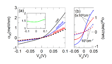
The calculated SOC coefficients for the InAs/InAsP CSNW of Fig. 1 as a function of the back gate voltage is reported in Fig. 2(a). The SOC constant is trivially zero if , due to the overall inversion symmetry. At any finite voltage the inversion symmetry is removed, hence . As shown in Fig. 2(a), the total ensues from two different contributons, namely interfacial and electrostatic, whose magnitude is of the same order. It is thus crucial to include both of them in the assessment of SOC in CSNWs. Note that the electrostatic component almost coincides with the value for an InAs NW with the same geometry, but no overgrown shell222For the model CSNW under consideration, the gate is attached directly to the NW, so that is an upper bound value, while any dielectric interlayer would decrease . For the NW with no shell, the gate has been placed at the same distance from the core as in the case with the shell, in other to compare the two calculations.. However, for this specific nanostructure, the largest part of is due to the interfacial contribution, which is larger than the electrostatic one. While the ratio between the two contributions is nearly independent of [see the inset in Fig. 2(a)], they are both strongly anisotropic with respect to the field direction. This is due to the different effects on the charge density, as discussed in Ref. Wójcik, Bertoni, and Goldoni, 2018a. This effect can also be grasped from the probability distribution reported in Fig. 3 (top and bottom rows). Indeed, the positive pushes electron states towards the interface opposite to the gate, where the gradient of the self-consistent field is low. On the other hand, at electrons are pulled to the region of the nearest interface with the stronger electric field, additionally strengthened by the electron-electron interactionWójcik, Bertoni, and Goldoni (2018a).
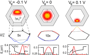
The value of depends on the penetration of the wave function into the interfaces. As shown in Fig. 3 (middle row) the linear density of interfacial SOC at the interfaces is finite almost everywhere, but it has opposite sign at opposite facets.333The sign of the SOC linear density on each facet is decided by the choice of the reference frame. Since appears combined with the spin matrices in the Hamiltonian (2), the overall sign of the SOC term is unaffected by a change in the reference frame. For a centro-symmetric system () the overall value is zero, since opposite contributions cancel out exactly. We stress a remarkable difference between CSNWs and analogous planar structures. In a planar asymmetric quantum well, for example, . In a CSNW with an embedded quantum well, however, the overall symmetry is recovered even if each facet of the quantum well is individually asymmetric. Therefore, opposite segments have opposite Rashba contributions and compensate. However, any asymmetric gate potential unbalances opposite contributions, the total effect being related to the amount of envelope function at the interface.
Note the almost linear increase of with . This behaviour is observed in a relatively small charge density regime: the average Coulomb energy is small, most of the charge is located in the core, and it is relatively rigid to an applied transverse electric field. At larger densities, however, charge moves at the interfaces to minimize Coulomb interaction Bertoni et al. (2011), with negligible tunneling energy between opposite facets. In this regime, the symmetric charge density distribution is unstable and it is easily distorted by an electric field Wójcik, Bertoni, and Goldoni (2018a). Accordingly, SOC constant shoots around as soon as the gate is switched on - see Fig. 2(b).
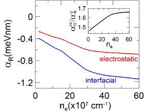
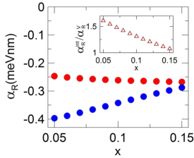
As we show in Fig. 4, both SOC components substantially increase in intensity with charge density, while their ratio is weakly affected, it being rather a property of the nano-material (band parameters and band offset). This is explicitly shown in Fig. 5, where the two contributions are plot vs the stechiometric fraction . At low , penetration is very large, and the interfacial effect is dominant (of course for the heterostructure is an homogeneous NW with a larger diameter), while as the two contributions are comparable, as also shown in the inset.
To summarize, we have shown that Rashba SOC in CSNWs is increased by the effect of the radial heterointerface, and its control via external metallic gates may be highly improved by this interfacial effect. Although we did not attempt to optimize in the many parameter space allowed by CSNWs, our results suggest that a general strategy to enhance SOC in CSNWs relies on a modification of the compositional structure exploiting asymmetric penetration of the wave function into the shell layer.
This work was partially supported by the AGH UST statutory tasks No. 11.11.220.01/2 within subsidy of the Ministry of Science and Higher Education and in part by PL-Grid Infrastructure. P.W. was supported by National Science Centre, Poland (NCN) according to decision 2017/26/D/ST3/00109.
References
- Kokurin (2015) I. A. Kokurin, Physica E 74, 264 (2015).
- Kokurin (2014) I. A. Kokurin, Solid State. Commun. 195, 49 (2014).
- Kammermeier et al. (2016) M. Kammermeier, P. Wenk, J. Schliemann, S. Heedt, and T. Schäpers, Phys. Rev. B 93, 205306 (2016).
- Winkler et al. (2017) G. W. Winkler, D. Varjas, R. Skolasinski, A. A. Soluyanov, M. Troyer, and M. Wimmer, Phys. Rev. Lett. 119, 037701 (2017).
- Wójcik, Bertoni, and Goldoni (2018a) P. Wójcik, A. Bertoni, and G. Goldoni, Phys. Rev. B 97, 165401 (2018a).
- Campos et al. (2018) T. Campos, P. E. Faria Junior, M. Gmitra, G. M. Sipahi, and J. Fabian, Phys. Rev. B 97, 245402 (2018).
- Luo, Li, and Zunger (2017) J.-W. Luo, S.-S. Li, and A. Zunger, Phys. Rev. Lett. 119, 126401 (2017).
- Alicea (2010) J. Alicea, Phys. Rev. B 81, 125318 (2010).
- Sau (2017) J. Sau, Physics 10, 68 (2017).
- Kitaev (2003) A. Kitaev, Ann. Phys. 303, 2 (2003).
- Sau, Tewari, and Das Sarma (2012) J. D. Sau, S. Tewari, and S. Das Sarma, Phys. Rev. B 85, 1 (2012).
- Mourik et al. (2012) V. Mourik, K. Zuo, S. M. Frolov, S. R. Plissard, E. P. A. M. Bakkers, and L. P. Kouwenhoven, Science 336, 1003 (2012).
- Mastomäki et al. (2017) J. Mastomäki, S. Roddaro, M. Rocci, V. Zannier, D. Ercolani, L. Sorba, I. J. Maasilta, N. Ligato, A. Fornieri, E. Strambini, and F. Giazotto, Nano Research 10, 3468 (2017).
- Albrecht et al. (2016) S. M. Albrecht, A. P. Higginbotham, M. Madsen, F. Kuemmeth, T. S. Jespersen, J. Nygåard, P. Krogstrup, and C. M. Marcus, Nature 531, 206 (2016).
- Manolescu et al. (2017) A. Manolescu, A. Sitek, J. Osca, L. m. c. Serra, V. Gudmundsson, and T. D. Stanescu, Phys. Rev. B 96, 125435 (2017).
- Fabian et al. (2007) J. Fabian, A. Matos-Abiague, C. Ertler, P. Stano, and I. Žutić, Acta Physica Slovaca 57, 565 (2007).
- Datta and Das (1990) S. Datta and B. Das, Appl. Phys. Lett. 56, 665 (1990).
- Schliemann, Egues, and Loss (2003) J. Schliemann, J. C. Egues, and D. Loss, Phys. Rev. Lett. 90, 146801 (2003).
- Wójcik and Adamowski (2016) P. Wójcik and J. Adamowski, Semicond. Sci. Technol. 31, 115012 (2016).
- Wójcik et al. (2014) P. Wójcik, J. Adamowski, B. J. Spisak, and M. Wołoszyn, J. Appl. Phys. 115, 104310 (2014).
- Wójcik and Adamowski (2017) P. Wójcik and J. Adamowski, Sci Rep 7, 45346 (2017).
- Das et al. (2012) P. P. Das, J. Bhandari, N abd Wan, M. Cahay, K. B. Chetry, R. S. Newrock, and S. T. Herbert, Nanotechnology 23, 215201 (2012).
- Debray, Rahman, and Muhammad (2009) P. Debray, S. Rahman, and M. Muhammad, Nature Nano Technol. 4, 759 (2009).
- Kohda et al. (2012) M. Kohda, S. Nakamura, Y. Nishihara, K. Kobayashi, T. Ono, J. O. Ohe, Y. Tokura, T. Mineno, and J. Nitta, Nature Communications 3, 1082 (2012).
- Rossella et al. (2014) F. Rossella, A. Bertoni, D. Ercolani, M. Rontani, L. Sorba, F. Beltram, and S. Roddaro, Nat. Nanotechnol. 9, 997 (2014).
- Iorio et al. (2018) A. Iorio, M. Rocci, L. Bours, M. Carrega, V. Zannier, L. Sorba, S. Roddaro, F. Giazotto, and E. Strambini, ArXiv e-prints (2018), arXiv:1807.04344 [cond-mat.mes-hall] .
- Rashba (1960) E. I. Rashba, Sov. Phys. Solid State 2, 1109 (1960).
- Dresselhaus (1955) G. Dresselhaus, Phys. Rev. 100, 580 (1955).
- van Weperen et al. (2015) I. van Weperen, B. Tarasinski, D. Eeltink, V. S. Pribiag, S. R. Plissard, E. P. A. M. Bakkers, L. P. Kouwenhoven, and M. Wimmer, Phys. Rev. B 91, 201413(R) (2015).
- Kammhuber et al. (2017) J. Kammhuber, M. C. Cassidy, F. Pei, M. P. Nowak, A. Vuik, D. Car, S. R. Plissard, E. P. A. M. Bakkers, M. Wimmer, and L. P. Kouwenhoven, Nat Commun. 8, 478 (2017).
- Scherübl et al. (2016) Z. Scherübl, G. m. H. Fülöp, M. H. Madsen, J. Nygård, and S. Csonka, Phys. Rev. B 94, 035444 (2016).
- Hansen et al. (2005) A. E. Hansen, M. T. Björk, C. Fasth, C. Thelander, and L. Samuelson, Phys. Rev. B 71, 205328 (2005).
- Dhara et al. (2009) S. Dhara, H. S. Solanki, V. Singh, A. Narayanan, P. Chaudhari, M. Gokhale, A. Bhattacharya, and M. M. Deshmukh, Phys. Rev. B 79, 121311 (2009).
- Roulleau et al. (2010) P. Roulleau, T. Choi, S. Riedi, T. Heinzel, I. Shorubalko, T. Ihn, and K. Ensslin, Phys. Rev. B 81, 155449 (2010).
- Estévez Hernández et al. (2010) S. Estévez Hernández, M. Akabori, K. Sladek, C. Volk, S. Alagha, H. Hardtdegen, M. G. Pala, N. Demarina, D. Grützmacher, and T. Schäpers, Phys. Rev. B 82, 235303 (2010).
- Wójcik, Bertoni, and Goldoni (2018b) P. Wójcik, A. Bertoni, and G. Goldoni, (2018b), unpublished.
- Kallaher et al. (2010a) R. L. Kallaher, J. J. Heremans, N. Goel, S. J. Chung, and M. B. Santos, Phys. Rev. B 81, 0035335 (2010a).
- Kallaher et al. (2010b) R. L. Kallaher, J. J. Heremans, N. Goel, S. J. Chung, and M. B. Santos, Phys. Rev. B 81, 075303 (2010b).
- Herling et al. (2017) F. Herling, C. Morrison, C. S. Knox, S. Zhang, O. Newell, M. Myronov, E. H. Linfield, and C. H. Marrows, Phys. Rev. B 95, 155307 (2017).
- Bertoni et al. (2011) A. Bertoni, M. Royo, F. Mahawish, and G. Goldoni, Phys. Rev. B 84, 205323 (2011).
- Funk et al. (2013) S. Funk, M. Royo, I. Zardo, D. Rudolph, S. Morkötter, B. Mayer, J. Becker, A. Bechtold, S. Matich, M. Döblinger, M. Bichler, G. Koblmüller, J. J. Finley, A. Bertoni, G. Goldoni, and G. Abstreiter, Nano Letters 13, 6189 (2013).
- Jadczak et al. (2014) J. Jadczak, P. Plochocka, A. Mitioglu, I. Breslavetz, M. Royo, A. Bertoni, G. Goldoni, T. Smolenski, P. Kossacki, A. Kretinin, H. Shtrikman, and D. K. Maude, Nano Letters 14, 2807 (2014).
- Royo, Bertoni, and Goldoni (2014) M. Royo, A. Bertoni, and G. Goldoni, Phys. Rev. B 89, 155416 (2014).
- Jabeen et al. (2008) F. Jabeen, S. Rubini, V. Grillo, L. Felisari, and F. Martelli, Appl. Phys. Lett. 93, 083117 (2008).
- Spirkoska et al. (2009) D. Spirkoska, J. Arbiol, A. Gustafsson, S. Conesa-Boj, F. Glas, I. Zardo, M. Heigoldt, M. H. Gass, A. L. Bleloch, S. Estrade, M. Kaniber, J. Rossler, F. Peiro, J. R. Morante, G. Abstreiter, L. Samuelson, and A. Fontcuberta i Morral, Phys. Rev. B 80, 245325 (2009).
- Devizorova and Volkov (2013) Z. A. Devizorova and V. A. Volkov, JETP Lett. 98, 101 (2013).
- Ivchenko, Kaminski, and Rössler (1996) E. L. Ivchenko, A. Y. Kaminski, and U. Rössler, Phys. Rev. B 54, 5852 (1996).
- Treu et al. (2013) J. Treu, M. Bormann, H. Schmeiduch, M. Döblinger, S. Morkötter, S. Matich, P. Wiecha, K. Saller, B. Mayer, M. Bichler, M.-C. Amann, J. J. Finley, G. Abstreiter, and G. Koblmüller, Nano Letters 13, 6070 (2013).
- Liu et al. (2013) X. Liu, P. Liu, H. Huang, C. Chen, T. Jin, Y. Zhang, X. Huang, Z. Jin, X. Li, and Z. Tang, Nanotechnology 24, 245306 (2013).
- Furthmeier et al. (2016) S. Furthmeier, F. Dirnberger, M. Gmitra, A. Bayer, M. Forsch, J. Hubmann, C. Schüller, E. Reiger, J. Fabian, T. Korn, and D. Bougeard, Nat Commun. 7, 12413 (2016).
- Sitek et al. (2018) A. Sitek, M. Urbaneja Torres, K. Torfason, V. Gudmundsson, A. Bertoni, and A. Manolescu, Nano Letters 18, 2581 (2018).
- Wong et al. (2011) B. M. Wong, F. Léonard, Q. Li, and G. T. Wang, Nano Letters 11, 3074 (2011).
- Royo et al. (2015) M. Royo, C. Segarra, A. Bertoni, G. Goldoni, and J. Planelles, Phys. Rev. B 91, 115440 (2015).
- de Andrada e Silva, La Rocca, and Bassani (1997) E. A. de Andrada e Silva, G. C. La Rocca, and F. Bassani, Phys. Rev. B 55, 16293 (1997).
- Note (1) Lattice mismatch and strain field are additional sources of SOC, which are neglected for the present lattice matched heterostructures. We also neglect a SOC contribution resulting from the interface inversion asymmetry related to different atomic termination at opposite interfaces Ivchenko, Kaminski, and Rössler (1996); Rössler and Kainz (2002) which is small. Moreover, additional calculations with slight smearing of the potential at the interface instead of the step like function did not lead to significantly different results.
- Vurgaftman, Meyer, and Ram-Mohan (2001) I. Vurgaftman, J. R. Meyer, and L. R. Ram-Mohan, J. Appl. Phys. 89, 5815 (2001).
- Note (2) For the model CSNW under consideration, the gate is attached directly to the NW, so that is an upper bound value, while any dielectric interlayer would decrease . For the NW with no shell, the gate has been placed at the same distance from the core as in the case with the shell, in other to compare the two calculations.
- Note (3) The sign of the SOC linear density on each facet is decided by the choice of the reference frame. Since appears combined with the spin matrices in the Hamiltonian (2), the overall sign of the SOC term is unaffected by a change in the reference frame.
- Ivchenko, Kaminski, and Rössler (1996) E. L. Ivchenko, A. Y. Kaminski, and U. Rössler, Phys. Rev. B 54, 5852 (1996).
- Rössler and Kainz (2002) U. Rössler and J. Kainz, Solid State Commun. 121, 313 (2002).