Best of Both Worlds: Integration of Split Manufacturing and Camouflaging into a Security-Driven CAD Flow for 3D ICs
Abstract.
With the globalization of manufacturing and supply chains, ensuring the security and trustworthiness of ICs has become an urgent challenge. Split manufacturing (SM) and layout camouflaging (LC) are promising techniques to protect the intellectual property (IP) of ICs from malicious entities during and after manufacturing (i.e., from untrusted foundries and reverse-engineering by end-users). In this paper, we strive for “the best of both worlds,” that is of SM and LC. To do so, we extend both techniques towards 3D integration, an up-and-coming design and manufacturing paradigm based on stacking and interconnecting of multiple chips/dies/tiers.
Initially, we review prior art and their limitations. We also put forward a novel, practical threat model of IP piracy which is in line with the business models of present-day design houses. Next, we discuss how 3D integration is a naturally strong match to combine SM and LC. We propose a security-driven CAD and manufacturing flow for face-to-face (F2F) 3D ICs, along with obfuscation of interconnects. Based on this CAD flow, we conduct comprehensive experiments on DRC-clean layouts. Strengthened by an extensive security analysis (also based on a novel attack to recover obfuscated F2F interconnects), we argue that entering the next, third dimension is eminent for effective and efficient IP protection.
1. Introduction
On the one hand, design practices by the industry attach importance to optimize for power, performance, and area (PPA) at the level of physical design or design architecture (e.g., cache hierarchies, speculative execution). On the other hand, researchers have demonstrated powerful attacks (e.g., Spectre (Kocher2018spectre, ) or side-channel leakage (lerman18, )) which leverage these very practices and optimization steps. Apart from such concerns regarding the security and trustworthiness of hardware at runtime, protecting the hardware itself from threats such as intellectual property (IP) piracy, illegal overproduction or insertion of hardware Trojans is another challenge (BRS17, ). Various design and manufacturing schemes have been put forth over the last decade, e.g., ranging from logic locking (yasin17_CCS, ; shamsi18_TIFS, ), layout camouflaging (rajendran13_camouflage, ; wang16_MUX, ; collantes16, ; nirmala16, ; Akkaya2018, ; chen15, ; patnaik17_Camo_BEOL_ICCAD, ; patnaik18_GSHE_DATE, ), to split manufacturing (rajendran13_split, ; wang17, ; patnaik_ASPDAC18, ; patnaik18_SM_DAC, ; wang18_SM, ; magana17, ; sengupta17_SM_ICCAD, ). The common theme among these techniques is that they incorporate security as a critical design parameter besides the traditional PPA metrics.
Independent of hardware security, 3D integration has made significant progress over recent years. 3D integration is to stack and interconnect multiple chips/dies/tiers, thereby promising to overcome the scalability bottleneck (“More-Moore”), which is further exacerbated by challenges for pitch scaling, routing congestion, process variations, et cetera (knechtel16_Challenges_ISPD, ; EF16, ). Recent studies and prototypes show that 3D integration can indeed offer significant benefits over conventional 2D chips (peng17, ; jung14, ; kim12_3dmaps, ). Besides, 3D integration advances manufacturing capabilities by various means such as parallel handling of wafers, higher yields due to smaller outlines of individual chips, and heterogeneous integration (“More-than-Moore”) (radojcic17, ).
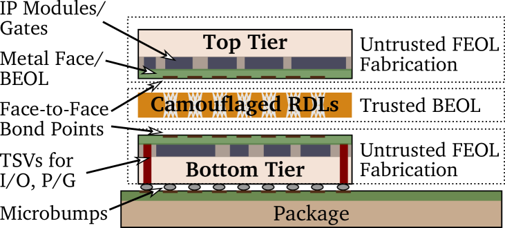
In this paper, we propose and evaluate a security-driven CAD flow for 3D ICs. We argue that 3D integration is an excellent candidate for IP protection, and we demonstrate that by combining layout camouflaging (LC) and split manufacturing (SM) naturally into one scheme (Fig. 1). This paper can be summarized as follows:
-
•
Initially, we review state-of-the-art approaches for LC and SM. We compare and contrast these schemes with regards to their security guarantees, shortcomings, and impact on PPA.
-
•
Next, we put forward a practical threat model which is in line with the present-day business models of design houses. This model necessitates both LC and SM in conjunction.
-
•
Most importantly, we demonstrate how 3D integration can help to achieve the “best of both worlds,” by combining the features of LC and SM. Thus, our scheme allows to inherently protect against IP piracy conducted by malicious entities during fabrication (untrusted foundries) and after fabrication (untrusted end-users). The key idea is to “3D split” the design into two tiers and to obfuscate the interconnects between those tiers. Towards this end, we propose a security-driven CAD and manufacturing flow for face-to-face (F2F) 3D ICs.
-
•
We implement our CAD flow using Cadence Innovus. We conduct a thorough analysis of DRC-clean layouts tailored for F2F 3D integration, and we contrast with the prior art of LC or SM (targeting on 2D/3D ICs) wherever applicable.
-
•
We present an extensive security analysis, underpinned by a novel proximity-centric attack on our security-driven 3D integration scheme. We provide both analytical and empirical data to showcase the resilience of our proposed schemes.
2. Background
2.1. Layout Camouflaging
Camouflaging (LC) is a layout-level technique to foil an adversary’s efforts for correctly inferring the design functionality while reverse engineering some chip. LC is accomplished during manufacturing by () dissolving optically distinguishable traits of standard cells, e.g., using look-alike gates (rajendran13_camouflage, ) or secretly configured MUXes (wang16_MUX, ), () using selective doping implantation for threshold-voltage-based obfuscation (collantes16, ; nirmala16, ; Akkaya2018, ), or () rendering the BEOL wires and/or vias resilient against reverse engineering (chen15, ; patnaik17_Camo_BEOL_ICCAD, ).
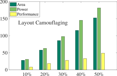
Existing schemes can incur significant PPA overheads once LC is applied for large parts of the design. For example for (rajendran13_camouflage, ), camouflaging 50% of the design results in 150% overheads for power and area, respectively (Fig. 2). Other emerging schemes such as threshold-voltage-based LC can suffer from massive PPA overheads as well; see Sec. 6 for more comparative results. Also note that most schemes require alterations to the FEOL manufacturing process, which can be costly. There, since camouflaging builds the secret for IP protection, the commissioned FEOL fab has to be trusted.
2.2. Split Manufacturing
Split manufacturing (SM) offers an interesting solution to safeguard the design IP during manufacturing time. Most commonly SM means that the device layer and few lower metal layers (front-end-of-line, FEOL) are fabricated using a high-end, potentially untrusted foundry, whereas the remaining interconnects (back-end-of-line, BEOL) are grown on top of the FEOL wafer by a trusted facility. The security promise lies in the fact that the untrusted foundry only holds a part of the overall design, making it difficult to infer the complete design functionality, and thereby hindering an adversary from IP piracy or targeted insertion of hardware Trojans.
Existing CAD tools, however, due to their focus on design closure (and their so-far agnostic view on security), tend to leave hints for an FEOL-based adversary. To honor PPA, for example, to-be-connected cells are typically placed close to each other. Hence, Rajendran et al. (rajendran13_split, ) proposed a so-called proximity attack which models this principle to infer the missing BEOL connections.
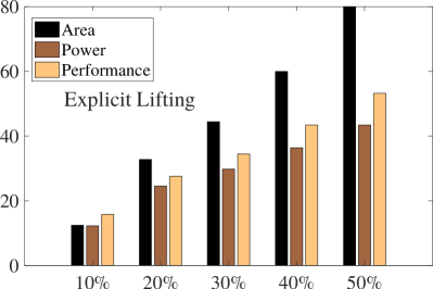
Various placement-centric (wang18_SM, ; sengupta17_SM_ICCAD, ; patnaik18_SM_DAC, ) and/or routing-centric (wang17, ; patnaik_ASPDAC18, ; patnaik18_SM_DAC, ) schemes have been proposed recently, which all aim to counter the efforts of various iterations of proximity attacks (wang18_SM, ; magana17, ). Among those defense schemes, lifting of wires above the split layer is an intuitive way to obfuscate the IP. That is, the revealing or critical wires (as selected by the designer) are lifted, e.g., with the help of routing pins in higher layers. In our exploratory experiments on randomized lifting of nets (Fig. 2), we observe steady increases in PPA cost. As with LC, more comparative results are given in Sec. 6.
2.3. 3D Integration and CAD Flows
3D integration can be classified into four flavors: (1) through-silicon via (TSV)-based 3D ICs, where chips are fabricated separately and then stacked, with inter-chip connections being realized by TSVs connected to metal layers; (2) face-to-face (F2F) stacking, where two tiers are fabricated separately and then bonded together at their metal faces; (3) monolithic 3D ICs, where multiple tiers are manufactured sequentially, with inter-tier connects based on regular metal vias; (4) 2.5D integration, where chips are fabricated separately and then bonded to a system-level interconnect carrier, the interposer. Each option has its scope, benefits and drawbacks, and requirements for CAD and manufacturing processes (knechtel16_Challenges_ISPD, ; knechtel17_TSLDM, ).
F2F stacking has arguably emerged as most promising (along with monolithic 3D ICs); various studies are actively streamlining efforts for commercial adoption (chang16, ; ku18, ; peng17, ; peng15_F2F, ). The principal goal of these studies is to optimize for PPA and the microarchitecture, not hardware security. More specifically, prior CAD flows carefully trade off intra-tier wiring with vertical interconnects across tiers. While the latter is the key feature of 3D integration, an overly large number of crossings/cuts has a significant impact on PPA as well. As we will explain in Sec. 6.3 in more detail, however, a large number of cuts is mandatory for a strong resilience against IP piracy.
3. A Practical Threat Model
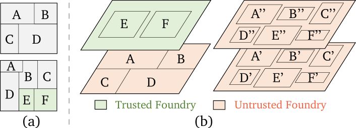
Here we put forward a novel, practical threat model for IP piracy, which is in line with the business models of present-day design houses. Consider the following scenario. A design house commissions an untrustworthy foundry to manufacture their newest version of some chip. This new version is typically extended from previous versions of the chip (Fig. 3)—the reuse of IP modules and the re-purposing of proven architectures are well-known principles. Hence, the previous versions of the chip can be obtained from the market. For example, think of the flagship iPhone® by Apple®. The iPhone 7, based on the A10 chip, was launched in September 2016, and the iPhone X, based on the successor chip A11, was launched in September 2017—both chips are available in the market. In this scenario, it is intuitive that recovering the new IP can become significantly less challenging for the potentially untrustworthy fab. In case the same fab was already commissioned for the previous version, it readily holds that prior layout; otherwise it can reverse engineer the layout from chips bought in the market. In any case, the adversaries can compare that prior layout with the new layout, to locate and focus on those parts which are different and unique.
Now, the conclusion for this thought experiment is that both SM and LC are required for manufacturing of all different chip versions. LC is required to prevent reverse engineering of the current layout by any other fab commissioned for later chip versions; SM is necessary to prevent the fab which is manufacturing the current version (and which is also tasked to implement LC) from readily inferring the complete layout of the current version. Prior art can only account for this practical threat model by applying both SM and LC, which can exacerbate the overheads and shortcomings as discussed in Sec. 2. Next, we outline our scheme to combine SM and LC naturally while leveraging 3D integration.
4. 3D Integration: Our Concept for IP Protection in the Next Dimension
The primary advancement we propose for SM is to “3D split” the design into multiple tiers. That is, unlike regular SM in 2D where the whole layout is split into FEOL and BEOL, here we split the layout itself into two parts. These two parts are manufactured as separate chips and then stacked and interconnected, in this paper based on the F2F flow. Our work is the first which demonstrates such a natural extension of SM.111We acknowledge that the idea for 3D SM was envisioned in 2008 by Tezzaron (tezzaron08, ). Also, there are studies hinting at the benefits of 3D integration for SM (dofe17, ; gu16, ; imeson13, ; xie17, ; valamehr13, ), but all have shortcomings or cover different scenarios: Dofe et al. (dofe17, ) and Gu et al. (gu16, ) remain on the conceptional level; Xie et al. (xie17, ) and Imeson et al. (imeson13, ) consider 2.5D integration where only wires are hidden from the untrusted foundry; Valamehr et al. (valamehr13, ) propose to stack customized monitoring circuitry on top of untrustworthy chips, i.e., they leverage 3D integration for runtime monitoring, not for IP protection. We suggest that 3D SM can be done either by different foundries or by one foundry (Fig. 3):
-
(1)
Different trusted and untrusted foundries: Here we delegate the manufacturing to one low-end but trusted and one high-end but untrusted foundry, both with FEOL/BEOL capabilities. A chip company may have significantly more options to commission a trustworthy foundry (or even manufacture in-house) in case the sought-after technology node is old yet still widely available, e.g., 180nm. While keeping one design part exclusively with a trusted foundry is promising security-wise, the practicality of this option seems limited.
-
(2)
Untrusted foundries/foundry: Here we commission only high-end but untrusted foundries for both parts/chips. This way, we may benefit from the latest technology node but, naturally, have to split the design in such a way that the foundries cannot readily infer the whole layout, even when they are colluding. Once such strong protection is in place, it is economically more reasonable to commission only one foundry.
4.1. Different Trusted and Untrusted Foundries
The commissioning of several foundries with different technologies and trust levels has some critical implications as follows.
First, regarding the practical threat model, it is straightforward to assign the new IP exclusively to the chip manufactured by the trusted foundry. As for the resilience of this inherently secure 3D SM scheme, there is no generic attack model in the literature yet which can account for this scenario, that is, when given only one part of the layout how to infer the missing connections and gates. We believe that a corresponding “black-box” attack would be very challenging, but we suggest that the community may consider it.
Second, due to the different pitches for different technologies, only a fraction of the design can be delegated to the low-end chip. That is at least as long as (a) the high-end chip shall have reasonable utilization for cost efficiency and (b) the outlines of both chips shall remain the same, which is a common requirement for 3D stacking.
Third, the overall power and performance is dominated by the low-end chip, where other factors such as parasitics may further exacerbate the overheads in practice (peng17, ).
In our exploratory experiments, we gauge the capabilities for such 3D SM, assuming a trusted 180nm foundry and an untrusted 45nm foundry. More specifically, we leverage the OSU libraries (OSU_PDK, ). Their libraries hold the same number, type, and strengths of cells; this guarantees a fair comparison since CAD tools cannot leverage different versions of cells. Synopsys DC was used for synthesis and place and route was performed using Cadence Innovus 17.1. PPA results for an aggressive timing closure of the 2D baseline setup are given in Table 1.222 The node 45nm is four generations away from 180nm, and delays improve by 30% per generation (borkar1999design, ); surprisingly, delay degradations for the OSU 180nm library are notably below such expectations. We believe that this is due the academic nature of the library. At the point of writing, we had no access to different commercial libraries. In any case, the key findings for our experiments remain valid. That is because once the delay numbers in the library would be revised, and still assuming the same types of cells are used, the overall delay would merely scale up linearly. For the heterogeneous F2F 3D setup (Fig. 4), we observe some performance degradation as we lift more gates to the low-end tier. Also, note from Table 1 that area (and power) cost is 12X (and 9X) when contrasting 180nm to 45nm. To maintain a balanced utilization for both tiers, these correlations imply that one should not lift more than 8% of the gates to the low-end tier. While such small-scale lifting provides a reasonable performance gain, especially from the perspective of commissioning only the 180nm foundry, it may not be enough to cover all the sensitive IP.
In short, we find that leveraging different foundries has practical limitations. Delegating more than 8% of the gates to the low-end foundry is ineffective, especially when considering that this foundry has to implement LC as well, which incurs further cost.
| Benchmark | 45nm | 180nm | ||||||
|---|---|---|---|---|---|---|---|---|
| # Instances | Area | Power | Delay | # Instances | Area | Power | Delay | |
| b17_1 | 14,850 | 32,770.28 | 8.85 | 2.29 | 14,711 | 417,416 | 71.54 | 3.59 |
| b20 | 6,959 | 15,549.31 | 8.12 | 2.87 | 7,521 | 216,168 | 97.94 | 3.6 |
| b21 | 7,327 | 16,096.05 | 8.79 | 2.88 | 7,060 | 203,216 | 85.66 | 3.89 |
4.2. Untrusted Foundries
Engaging with several untrusted foundries offering the same technology (or one untrusted foundry) also holds some key implications.
First, power and performance of such “conventional 3D ICs” can be expected to excel those of the different-technology scenario above. In fact, folding (or splitting) of 2D IP modules within 3D ICs has been successfully demonstrated for some time (lin16, ; jung14, ; jung17, ; peng15_F2F, ), albeit without IP piracy in mind. Hence, savings from the folding of IP modules may provide some margin for a defense scheme, but we show in the remainder of this work that this margin naturally depends on the design and the measures applied for protection.
Second, although IP modules can be folded/split across tiers, which may mislead a reverse-engineering attacker, both tiers are still manufactured by untrusted foundries. This fact implies that LC schemes targeting on the device level cannot help to protect the IP from adversaries in those foundries. Interestingly, there is another LC flavor emerging, that is the obfuscation of interconnects (cocchi14, ; chen15, ; vijayakumar16, ; patnaik17_Camo_BEOL_ICCAD, ). Chen et al. (chen15, ) consider real and dummy vias using magnesium, Mg and magnesium-oxide, MgO, respectively. They demonstrate that real Mg vias oxidize quickly into MgO and, hence, can become indistinguishable from the other MgO dummy vias during reverse engineering. Hwang et al. (hwang12_transient_electronics, ) have shown that Mg and MgO dissolve quickly when surrounded by fluids, which is inevitable in etching procedures applied for reverse engineering. Thus, without loss of generality, we assume our interconnect obfuscation to be based on the use of Mg/MgO vias.
We argue that the obfuscation of interconnects is a natural match for F2F 3D ICs—in between the tiers, further redistribution layers (RDLs) can be purposefully manufactured for obfuscation. Doing so only requires a trustworthy BEOL facility, which is a practical assumption given that BEOL fabrication is much less demanding than FEOL fabrication, especially for higher metal layers (RDLs reside between the F2F bonds which themselves are at higher layers).
5. Methodology
Here we elaborate on the CAD and manufacturing flow for our notion of security-driven F2F stacking. The CAD flow is in parts inspired by Chang et al. (chang16, ), but we devise our flow with a particular focus on IP protection (Fig. 5). Our flow allows a concerned designer to explore the trade-offs between PPA and cuts, i.e., the number of F2F inter-tier connections. Cuts are a crucial metric for the security analysis, which is discussed in more detail in Sec 6.3. It is also important to note that we follow the call for layout anonymization (imeson13, )—we purposefully do not engage cross-tier optimization steps, to mitigate layout-level hints on the obfuscated BEOL/RDLs.
As for the F2F process, we propose the following security-driven modification. The wafers for the two tiers are fabricated by one (two) untrusted foundry (foundries) and then shipped to a trusted BEOL and stacking facility. This trusted facility grows the obfuscated RDLs on top of one wafer, and continues with the regular F2F flow (i.e., flipping and bonding the second wafer on top).
5.1. Design Partitioning
After obtaining the post-routed 2D design, we partition the netlist into top and bottom groups, representing the tiers of the F2F IC. I/O ports are created for all interconnects between the two groups, representing the F2F vias. Besides these F2F ports, we place primary I/Os at the chip boundary, as in conventional 2D designs. (This is also practical for F2F integration where TSVs are to be manufactured at the chip boundary for primary I/Os and the P/G grid.)
Random partitioning: A naive way for security-driven partitioning is to assign gates to the top/bottom groups randomly. When doing so, the number of cuts will be dictated by the number, type, and local interconnectivity of gates being assigned to one group.
Maximizing the cut-size: As already indicated (and further explored in Sec 6.3), the larger the cut size, the more difficult becomes IP piracy. Hence, here we seek to increase the cut size as much as reasonably possible. First, timing reports for the 2D baseline are obtained. Next, gates are randomly alternated along their timing paths towards the top/bottom groups. In the security-wise best case (which is also the worst-case regarding power and performance), every other gate is assigned to the top and bottom group, respectively; for a path with gates, cuts are arising.
Timing-aware partitioning: Here we seek to reduce layout cost while maintaining strong protection. First, the available timing slack is determined for each gate. Then, based on a user-defined threshold, the critical gates remain in the bottom tier, whereas all other gates are moved to the top tier. This procedure is repeated with revised timing thresholds until an even utilization for both tiers is achieved. Note that it is not easy for an attacker to understand whether any path in the bottom/top group is critical or not (or complete, for that matter). In other words, the attacker has to tackle both groups at once and, more importantly, resolve the randomized F2F vias and the obfuscated interconnects (see below).
5.2. Planning of F2F Interconnects
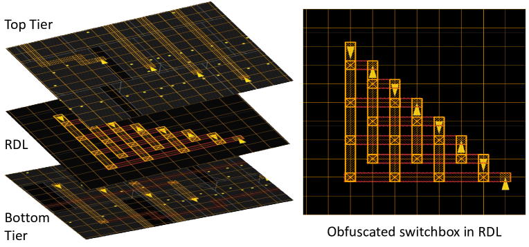
After placing the bottom tier, the initial locations for F2F ports are determined in the vicinity of the drivers/sinks. Then, a security-driven, i.e., randomized placement of F2F ports is conducted, along with customized on-track legalization. Next, obfuscated switchboxes are placed, and the F2F ports are mapped to the top tier.
Randomization: It is easy to see that regular planning of F2F interconnects cannot be secure, as this aligns the ports for the bottom and top tier directly. Hence, we randomize the arrangement of F2F ports as follows. (Fig. 6). We place additional F2F ports randomly (yet with the help of the on-track legalization) in the top RDL. These randomized ports are then routed through the RDLs towards the original F2F ports connecting with the bottom tier, which are also embedded into custom switchboxes (see next).
Obfuscated switchboxes: To protect against reverse engineering, we obfuscate the connectivity in the RDLs using a custom switchbox (Fig. 7). This switchbox allows stealthy one-to-one mapping of four drivers to four sinks. The essence of the switchbox are Mg/MgO vias (chen15, ), to cloak which driver connects to which sink. The pins of the switchbox represent the F2F ports. To enable proper utilization of routing resources, the pins are aligned with the routing tracks. For randomization, the additional ports connecting with the top tier are used for rerouting during design closure.
On-track legalization: Each F2F port is moved inside the core boundary, towards the center point defined by all instances connected with this port. Next, we obtain the closest and still-unoccupied on-track locations for actual placement. If need be, we stepwise increase the search radius considering a user-defined threshold.
5.3. Design Closure
After the F2F via planning stage, both tiers are placed and routed separately. Here we do not engage in any cross-tier optimization, to anonymize the individual tiers from each other, but we apply intra-tier optimization. While routing the bottom tier, we also route the randomized and obfuscated RDL with their switchboxes. Next, we encapsulate the top and bottom partitions in a wrapper netlist, and we assemble and implement the design followed by generating a SPEF file that captures the RC parasitics of the F2F vias. Finally, we perform DRC checks, evaluate the PPA, and stream out separate DEF files for the top/bottom tiers and the RDL.
6. Results
6.1. Experimental Setup
Implementation and layout evaluation: Our CAD flow is based on Cadence Innovus 17.1, using custom Tcl and Python scripts, which impose negligible runtime overheads. We use the Nangate 45nm library (nangate11, ) for our experiments, with six metal layers for the baseline 2D setup and six layers for the top and bottom tier each in the F2F setup. The RDL comprises four duplicated layers of M6, and F2F vias are modeled as M6 vias. (While this is an optimistic assumption, for now, F2F scaling can be expected to reach such dimensions.) The PPA analysis is conducted for the slow process corner at 0.95V V. For power analysis, we assume a switching activity of 0.2 for all primary inputs. We ensure that the layouts are free of any congestion, by choosing appropriate utilization rates. All experiments are carried out on an Intel Xeon E5-4660 @ 2.2 GHz with CentOS 6.9. For Cadence Innovus, up to 16 cores are allocated.
Setup for security evaluation: Since we promote 3D SM, regular proximity attacks such as (wang18_SM, ; magana17, ) cannot be applied. Thus, we propose (and publicly release (webinterface, )) a novel attack against 3D SM, also accounting for the RDL obfuscation underlying in our scheme; see also Sec. 6.3. The strength of our attack is evaluated by commonly used metrics, i.e., the correct connection rate (CCR) and Hamming distance (HD). HD is calculated using Synopsys VCS with 1,000,000 test patterns. As for SAT-based reverse engineering attacks, we leverage (subramanyan15, ). The related time-out is set to 72 hours.
Designs: Benchmarks from the ISCAS-85 and ITC-99 suites are used for layout and security analysis.
6.2. Security-Driven Layout Evaluation
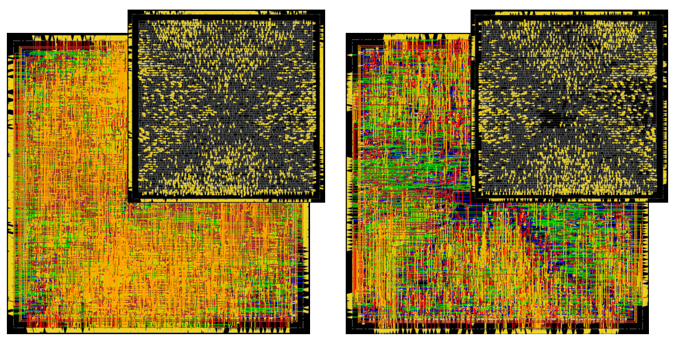
Our flow allows to trade off PPA and cuts; the latter dictates the resilience against IP piracy both during and after manufacturing. Figure 8 showcases the layout images for benchmark b22.
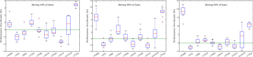
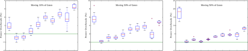
Maximizing the cut-size: Here we move gates from the bottom to the top group in steps of 10%, up to 50%. As the strategy is randomized, we perform ten runs for each benchmark for any given percentage of gates to move. The resulting power and performance distributions are illustrated in Fig. 9. Interestingly, even for the security-wise best case of randomly moving 50% of the gates, some runs still provide better power and/or performance than the 2D baseline. This finding demonstrates the potential for our scheme. Note that we refrain both from randomizing the F2F ports and from using the obfuscated switchboxes for these initial experiments.
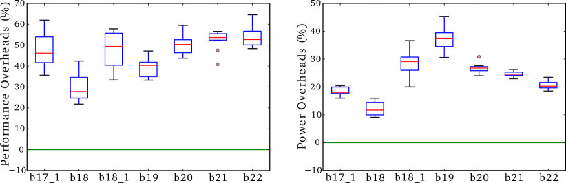
Once F2F ports are randomized and switchboxes are used, larger benchmarks such as b18_1 may incur overheads of up to 60% (Fig. 10). Hence, although this strategy offers strong resilience, a more aggressive PPA-security trade-off may be desired.
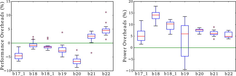
Timing-aware partitioning with F2F randomization and obfuscated switchboxes: This setup tackles the need outlined above. In fact, we observe that even for larger benchmarks (Fig. 11), there can be some layout benefits when comparing these 3D designs to their 2D baseline. To demonstrate the security implication of this setup, we plot the normalized distances between to-be-connected F2F vias in Fig. 6. This figure shows a wide variation across the inter-tier nets, whereas for regular/unprotected F2F stacking the distances would be all zero. For a more detailed security analysis, see Sec 6.3. Next, we compare our work to prior art.
Comparison with LC schemes: Threshold-based LC is recently gaining traction. Although promising in terms of resilience (for some schemes even during manufacturing), the PPA overheads are considerable. For example, Akkaya et al. (Akkaya2018, ) report overheads of 9.2, 6.6, and 3.3 for PPA, respectively, when compared to conventional 2-input NAND gate. Nirmala et al. (nirmala16, ) report 11.2 and 10.5 cost for power and area, respectively. Collantes et al. (collantes16, ) report power and performance cost of 72% and 31%, respectively, for 40% camouflaging. In (DBLP:journals/corr/JangG17, ), threshold voltages are leveraged to obfuscate the interconnects, leading to PPA overheads of 29%, 44%, and 33%, namely when 15% of the nets are obfuscated. In (patnaik17_Camo_BEOL_ICCAD, ), PPA overheads of 4.9%, 31.2%, and 25% are reported for b17 at 60% LC (by obfuscation of the interconnects). Even when compared to the latter more promising schemes, we can provide significantly better PPA (except for (patnaik17_Camo_BEOL_ICCAD, ) concerning power).
Dofe, Yan, et al. (dofe16_mono3D, ; yan17_camo, ) recently proposed LC for monolithic 3D ICs. At the time of writing, their libraries were not available to us for a detailed comparison. More importantly, however, manufacturing of such camouflaged 3D ICs requires trust into an advanced fab. The notion of 3D SM as in our scheme cannot be applied for monolithic 3D ICs (due to the sequential manufacturing process) and, thus, their scheme (dofe16_mono3D, ; yan17_camo, ) cannot protect the IP at manufacturing time.
Comparison with SM schemes: In Table 2, we compare with some studies on 2D SM. Overall, the placement-centric techniques by Wang et al. (wang18_SM, ) are competitive concerning power and performance. However, as is always the case for regular SM, Wang et al. can only avert fab-based adversaries, but not malicious end-users.
| Benchmark | BEOL+Physical (wang18_SM, ) | Logic+Physical (wang18_SM, ) | Logic+Logic (wang18_SM, ) | Concerted Lifting (patnaik_ASPDAC18, ) | Proposed with Random Partitioning | ||||||||||
| Area | Power | Delay | Area | Power | Delay | Area | Power | Delay | Area | Power | Delay | Area∗ | Power | Delay | |
| c432 | N/A | 0.17 | 0.49 | N/A | 0.44 | 0.24 | N/A | 0.17 | 0.21 | 7.7 | 13.1 | 11.6 | -50 | -2.66 | 0.31 |
| c880 | N/A | 0.25 | 0.05 | N/A | 0.35 | 0.03 | N/A | -0.05 | -0.09 | 0 | 12.1 | 19.9 | -50 | 0.97 | 1.6 |
| c1355 | N/A | 0.52 | 0.57 | N/A | 0.75 | 0.42 | N/A | 0.03 | 0.01 | 0 | 12.2 | 21.3 | -50 | 1.83 | 0.38 |
| c1908 | N/A | 1.1 | 1.3 | N/A | 1.1 | 0.23 | N/A | 0.45 | 0.39 | 7.7 | 14.6 | 18.9 | -50 | 0.11 | 1.69 |
| c2670 | N/A | 0.29 | 0.27 | N/A | 0.29 | 0.27 | N/A | 0.05 | 0.03 | 7.7 | 10 | 12 | -50 | -2.18 | 3.32 |
| c3540 | N/A | 0.53 | 0.28 | N/A | 0.36 | 0.02 | N/A | 0.14 | -0.02 | 7.7 | 5 | 2.8 | -50 | 0.59 | 4.32 |
| c5315 | N/A | 0.19 | -0.01 | N/A | 0.67 | 0.08 | N/A | 0.29 | -0.01 | 7.7 | 7.9 | 16.9 | -50 | -1.66 | 4.73 |
| c6288 | N/A | 0.29 | 0.19 | N/A | 0 | 0 | N/A | 0.1 | 0.67 | 27.3 | 12.3 | 15.7 | -50 | 10.43 | 10.21 |
| c7552 | N/A | 0.28 | -0.36 | N/A | 0.35 | -0.05 | N/A | 0.56 | 1.77 | 16.7 | 9.3 | 15.7 | -50 | 10.57 | 8.21 |
| Average | N/A | 0.4 | 0.31 | N/A | 0.48 | 0.14 | N/A | 0.19 | 0.33 | 9.2 | 10.7 | 15 | -50 | 2 | 3.86 |
∗Following the standard practice for 3D studies, we report on area by considering individual die outlines. In (patnaik_ASPDAC18, ), area is reported in terms of die outlines as well.
In Table 3, we compare with the security-driven 2.5D integration scheme by Xie et al. (xie17, ). Their work is relevant as they propose a similar notion of security based on cut sizes. For the benchmarks the authors considered, we obtain on average 53% more cuts in our scheme. (For our cut sizes for larger benchmarks, refer to Table 4). Regarding PPA, we observe significantly lower costs than (xie17, ).333 Concerning area, note that we report on die outlines, which is standard practice for 3D studies. Accordingly, for our numbers of -50%, the F2F 3D IC and the 2D baseline require the same total silicon area, i.e., we incur 0% absolute area cost. While Xie et al. report similar cost, they omit that their scheme requires an interposer which—being at least as large as the chips stacked onto it—incurs 100% cost. Still, mainly comprising metal layers, we acknowledge that an interposer is less expensive than regular chips. Besides, as with regular SM, their 2.5D scheme is not inherently resilient against malicious end-users, but our 3D scheme is.
6.3. Security Analysis and Attacks
Proximity attack for 3D SM: To the best of our knowledge, there is no attack yet in the literature which can account for 3D SM. Hence, we propose and implement such an attack, with a focus on one untrusted foundry (or two colluding foundries) and our RDL obfuscation. We provide this attack as a public release in (webinterface, ).
We assume that the attacker holds the layout files for the top and bottom tier, but initially she has no access to the trusted RDL (we discuss the implications for obtaining the RDL further below). Although she understands how many drivers are connecting from the bottom to the top tier and vice versa, she does not know which driver connects to which sink, given the randomized F2F vias. Recall that we do not engage in cross-tier optimization, to mitigate any layout-level hints.444Also recall the different-foundries scenario in Sec. 4.1, which is significantly more challenging. There, the attacker has not only to tackle the driver-sink mappings but furthermore guess the set of gates withhold by the trusted foundry. Let us assume there are drivers in the bottom and drivers in the top tier. Since we do not allow for fan-outs within the RDL (as this would occupy more F2F vias than necessary), there are only one-to-one mappings—this results in possible netlists. Once switchboxes are used, however, the attacker can tackle groups of four drivers/sinks at once. Still, she has to resolve (a) which four top-tier drivers are connected to which four bottom-tier sinks and vice versa, and (b) the connectivity within the obfuscated switchboxes. For those cases, there are possible netlists remaining. Next, we outline the corresponding heuristics at the heart of our attack.
-
(1)
Unique mappings: Any driver in the bottom/top tier will feed only one sink in the top/bottom tier. Hence, an attacker will reconnect drivers and sinks individually. Moreover, she can identify all primary I/Os as they are implemented using wirebonds or TSVs, not randomized F2F vias.
-
(2)
Layout hints: Although the F2F vias are randomized, the attacker may try to correlate the proximity and orientation of F2F vias with their corresponding but withheld RDL connectivity. Towards this end, she can also leverage the routing towards the switchbox ports. Moreover, recalling the practical threat model, the attacker may be able to identify some known IP and accordingly confine the related sets of candidate F2F interconnects. Our attack is generic and can account for those scenarios, by keeping track of the candidate F2F pairings considered by the attacker.
-
(3)
Combinatorial loops: Since both tiers and thus all active components are available to the attacker, she can readily exclude those F2F connections inducing combinatorial loops.
We provide empirical attack results in Table 4. Here we assume that the attacker was able to correctly infer all the driver-sink pairings through the switchboxes, only the obfuscation within switchboxes themselves remains to be attacked. This is a strong assumption and rendering our evaluation conservative. In fact, this scenario can be considered as an optimal proximity attack, as for all F2F connections the correct one is always among the considered candidates. The results in Table 4 indicate the computational efficiency of our attack for smaller designs, but also the challenges once larger designs with large solution spaces are to be tackled. With regards to CCR and HD for the successfully recovered netlists, our protection scheme can be considered as reasonably secure.
| Benchmark | Xie et al. (xie17, ) (SC+SP) | Proposed with Random Partitioning | ||||||
| Cut Size | Area | Power | Delay | Cut Size | Area | Power | Delay | |
| c432 | 130 | 1 | 17.6 | 5.9 | 134 | -50 (0) | -2.66 | 0.31 |
| c880 | 141 | 0 | 29.4 | 10 | 138 | -50 (0) | 0.97 | 1.6 |
| c1355 | 130 | 0 | 17.6 | 17.6 | 91 | -50 (0) | 1.83 | 0.38 |
| c1908 | 132 | 1 | 11.8 | 29.4 | 149 | -50 (0) | 0.11 | 1.69 |
| c2670 | 152 | 0 | 11.8 | 5.9 | 154 | -50 (0) | -2.18 | 3.32 |
| c3540 | 133 | 0 | 5.9 | 5.9 | 349 | -50 (0) | 0.59 | 4.32 |
| c7552 | 157 | 1 | 1 | 5.9 | 477 | -50 (0) | 10.57 | 8.21 |
| Average | 139 | 0.4 | 13.6 | 11.5 | 213 | -50 (0) | 1.32 | 2.83 |
| Benchmark | Cut Sizes | SAT Attack (subramanyan15, ) | Proposed 3D-SM Proximity Attack | |||
| Random | Timing-Aware | Runtime (Min.) | CCR (%) | HD (%) | Runtime (Sec.) | |
| c432 | 134 | 56 | 624 | 30.4 | 45.2 | 10 |
| c880 | 138 | 53 | 642 | 27.8 | 39.4 | 23 |
| c1355 | 91 | 37 | 492 | 31.1 | 43.8 | 53 |
| c3540 | 349 | 97 | 948 | 22.6 | 41.3 | 3,729 (62 Minutes) |
| b17_1 | 6,650 | 2,482 | t-o | N/A | N/A | t-o |
| b18 | 15,974 | 6,906 | t-o | N/A | N/A | t-o |
| b18_1 | 16,706 | 6,616 | t-o | N/A | N/A | t-o |
| b19 | 33,417 | 13,142 | t-o | N/A | N/A | t-o |
SAT-based attack: After manufacturing, the attacker can readily understand which four drivers/sinks are connected through the switchboxes, but she still has to resolve the obfuscation within the switchboxes themselves. The attacker may now leverage a working copy as an oracle and launch a SAT attack. Towards that end, we employ the attack proposed in (subramanyan15, ), and we model the problem using multiplexers as outlined in (massad15, ; yu17, ). Empirical results are given in Table 4. As expected, the SAT attack succeeds for smaller designs but runs into time-out for larger designs. This finding is also consistent with those reported by Xie et al. (xie17, ) for their security-driven 2.5D scheme, which has a security notion similar to our work.
7. Conclusion and Outlook
Initially, we review prior art and their limitations. We also put forward a novel, practical threat model of IP piracy which is in line with the business models of present-day chip companies. Next, we elaborate in detail how 3D integration is a naturally strong match to combine SM and LC. (This also allows us to extend the defense scope of SM to practical commercial applications.) Towards this end, we propose a security-driven CAD and manufacturing flow for face-to-face (F2F) ICs, an up-and-coming option for 3D integration. We conduct comprehensive experiments on DRC-clean layouts, and strengthened by an extensive security analysis, we argue that entering the third dimension is promising for IP protection.
As for future work, we aim for a more formal method for partitioning gates across tiers, also to protect against other threats such as hardware Trojans. In the broader sense, we plan to explore if and how 3D integration can provide resilience against physical attacks such as invasive probing or exploitation of side-channel leakage.
Acknowledgments
This work was supported in part by the Center for Cyber Security (CCS) at NYU New York/Abu Dhabi (NYU/NYUAD). We also thank Dr. Anja Henning-Knechtel for preparing selected illustrations.
References
- (1) P. Kocher et al., “Spectre attacks: Exploiting speculative execution,” in Proc. S&P, 2019.
- (2) L. Lerman et al., “Start simple and then refine: Bias-variance decomposition as a diagnosis tool for leakage profiling,” Trans. Comp., vol. 67, no. 2, pp. 268–283, 2018.
- (3) S. Bhunia, S. Ray, and S. Sur-Kolay, Eds., Fundamentals of IP and SoC Security. Springer, 2017.
- (4) M. Yasin et al., “Provably-secure logic locking: From theory to practice,” in Proc. CCS, 2017, pp. 1601–1618.
- (5) K. Shamsi et al., “On the approximation resiliency of logic locking and IC camouflaging schemes,” Trans. IFS, 2018.
- (6) J. Rajendran et al., “Security analysis of integrated circuit camouflaging,” in Proc. CCS, 2013, pp. 709–720.
- (7) X. Wang et al., “Secure and low-overhead circuit obfuscation technique with multiplexers,” in Proc. GLSVLSI, 2016, pp. 133–136.
- (8) M. I. M. Collantes, M. E. Massad, and S. Garg, “Threshold-dependent camouflaged cells to secure circuits against reverse engineering attacks,” in Proc. ISVLSI, 2016, pp. 443–448.
- (9) I. R. Nirmala et al., “A novel threshold voltage defined switch for circuit camouflaging,” in Proc. ETS, 2016, pp. 1–2.
- (10) N. E. C. Akkaya, B. Erbagci, and K. Mai, “A secure camouflaged logic family using post-manufacturing programming with a 3.6GHz adder prototype in 65nm CMOS at 1V nominal VDD,” in Proc. ISSCC, 2018, pp. 128–130.
- (11) S. Chen et al., “Chip-level anti-reverse engineering using transformable interconnects,” in Proc. DFT, 2015, pp. 109–114.
- (12) S. Patnaik et al., “Obfuscating the interconnects: Low-cost and resilient full-chip layout camouflaging,” in Proc. ICCAD, 2017, pp. 41–48.
- (13) S. Patnaik et al., “Advancing hardware security using polymorphic and stochastic spin-hall effect devices,” in Proc. DATE, 2018, pp. 97–102.
- (14) J. Rajendran, O. Sinanoglu, and R. Karri, “Is split manufacturing secure?” in Proc. DATE, 2013, pp. 1259–1264.
- (15) Y. Wang et al., “Routing perturbation for enhanced security in split manufacturing,” in Proc. ASPDAC, 2017, pp. 605–610.
- (16) S. Patnaik et al., “Concerted wire lifting: Enabling secure and cost-effective split manufacturing,” in Proc. ASPDAC, 2018, pp. 251–258.
- (17) S. Patnaik et al., “Raise your game for split manufacturing: Restoring the true functionality through BEOL,” in Proc. DAC, 2018, pp. 140:1–140:6.
- (18) Y. Wang et al., “The cat and mouse in split manufacturing,” Trans. VLSI, vol. 26, no. 5, pp. 805–817, 2018.
- (19) J. Magaña et al., “Are proximity attacks a threat to the security of split manufacturing of integrated circuits?” Trans. VLSI, vol. 25, no. 12, 2017.
- (20) A. Sengupta et al., “Rethinking split manufacturing: An information-theoretic approach with secure layout techniques,” in Proc. ICCAD, 2017, pp. 329–336.
- (21) J. Knechtel and J. Lienig, “Physical design automation for 3D chip stacks – challenges and solutions,” in Proc. ISPD, 2016, pp. 3–10.
- (22) I. A. M. Elfadel and G. Fettweis, Eds., 3D Stacked Chips – From Emerging Processes to Heterogeneous Systems. Springer, 2016.
- (23) Y. Peng et al., “Parasitic extraction for heterogeneous face-to-face bonded 3-D ICs,” Trans. CPMT, vol. 7, no. 6, pp. 912–924, 2017.
- (24) M. Jung et al., “On enhancing power benefits in 3D ICs: Block folding and bonding styles perspective,” in Proc. DAC, 2014, pp. 1–6.
- (25) D. H. Kim et al., “3D-MAPS: 3D massively parallel processor with stacked memory,” in Proc. ISSCC, 2012, pp. 188–190.
- (26) R. Radojcic, More-than-Moore 2.5D and 3D SiP Integration. Springer, 2017.
- (27) J. Knechtel et al., “Large-scale 3D chips: Challenges and solutions for design automation, testing, and trustworthy integration,” Trans. SLDM, vol. 10, pp. 45–62, 2017.
- (28) K. Chang et al., “Cascade2D: A design-aware partitioning approach to monolithic 3D IC with 2D commercial tools,” in Proc. ICCAD, 2016, pp. 130:1–130:8.
- (29) B. W. Ku, K. Chang, and S. K. Lim, “Compact-2D: A physical design methodology to build commercial-quality face-to-face-bonded 3D ICs,” in Proc. ISPD, 2018, pp. 90–97.
- (30) Y. Peng et al., “Thermal impact study of block folding and face-to-face bonding in 3D IC,” in Proc. IITC, 2015, pp. 331–334.
- (31) Tezzaron Semiconductor, “3D-ICs and integrated circuit security,” Tezzaron Semiconductor, Tech. Rep., 2008. [Online]. Available: http://tezzaron.com/media/3D-ICs_and_Integrated_Circuit_Security.pdf
- (32) J. Dofe et al., “Security threats and countermeasures in three-dimensional integrated circuits,” in Proc. GLSVLSI, 2017, pp. 321–326.
- (33) P. Gu et al., “Leveraging 3D technologies for hardware security: Opportunities and challenges,” in Proc. GLSVLSI, 2016, pp. 347–352.
- (34) F. Imeson et al., “Securing computer hardware using 3D integrated circuit (IC) technology and split manufacturing for obfuscation,” in Proc. USENIX, 2013, pp. 495–510.
- (35) Y. Xie, C. Bao, and A. Srivastava, “Security-aware 2.5D integrated circuit design flow against hardware IP piracy,” Computer, vol. 50, no. 5, pp. 62–71, 2017.
- (36) J. Valamehr et al., “A 3-D split manufacturing approach to trustworthy system development,” Trans. CAD, vol. 32, no. 4, pp. 611–615, 2013.
- (37) (2017) FreePDK: Unleashing VLSI to the Masses. Oklahoma State University. [Online]. Available: https://vlsiarch.ecen.okstate.edu/flows/
- (38) S. Borkar, “Design challenges of technology scaling,” Micro, vol. 19, no. 4, pp. 23–29, 1999.
- (39) J.-M. Lin, P.-Y. Chiu, and Y.-F. Chang, “SAINT: Handling module folding and alignment in fixed-outline floorplans for 3D ICs,” in Proc. ICCAD, 2016.
- (40) M. Jung et al., “Design methodologies for low-power 3-D ICs with advanced tier partitioning,” Trans. VLSI, vol. 25, no. 7, 2017.
- (41) R. P. Cocchi et al., “Circuit camouflage integration for hardware IP protection,” in Proc. DAC, 2014, pp. 1–5.
- (42) A. Vijayakumar et al., “Physical design obfuscation of hardware: A comprehensive investigation of device- and logic-level techniques,” Trans. IFS, vol. 12, pp. 64–77, 2017.
- (43) S.-W. Hwang et al., “A physically transient form of silicon electronics,” Science, vol. 337, no. 6102, pp. 1640–1644, 2012.
- (44) (2011) NanGate FreePDK45 Open Cell Library. Nangate Inc. [Online]. Available: http://www.nangate.com/?page_id=2325
- (45) (2018) DfX Lab, NYUAD. [Online]. Available: http://sites.nyuad.nyu.edu/dfx/research-topics/design-for-trust-split-manufacturing/
- (46) P. Subramanyan, S. Ray, and S. Malik, “Evaluating the security of logic encryption algorithms,” in Proc. HOST, 2015, pp. 137–143.
- (47) J. Jang and S. Ghosh, “A novel interconnect camouflaging technique using transistor threshold voltage,” arXiv, vol. abs/1705.02707, 2017.
- (48) J. Dofe et al., “Transistor-level camouflaged logic locking method for monolithic 3D IC security,” in Proc. AHOST, 2016, pp. 1–6.
- (49) C. Yan et al., “Hardware-efficient logic camouflaging for monolithic 3D ICs,” Trans. CS, vol. 65, no. 6, pp. 799–803, 2018.
- (50) M. E. Massad, S. Garg, and M. V. Tripunitara, “Integrated circuit (IC) decamouflaging: Reverse engineering camouflaged ICs within minutes,” in Proc. NDSS, 2015, pp. 1–14.
- (51) C. Yu et al., “Incremental SAT-based reverse engineering of camouflaged logic circuits,” Trans. CAD, vol. 36, no. 10, pp. 1647–1659, 2017.