Customisable X-ray fluorescence photodetector with submicron sensitivity
using a ring array of silicon p-i-n diodes
Abstract
The research and development of silicon-based -ray fluorescence detectors achieved its submicron sensitivity. Its initial use is intended for in-situ beam monitoring at advanced light-source facilities. The effectively functioning prototype fully leveraged technologies and techniques from a wide array of scientific disciplines: -ray fluorescence technique, photon scattering and spectroscopy, astronomical photometry, semiconductor physics, materials science, microelectronics, analytical and numerical modelling, and high-performance computing. In the design stage, the systematic two-track approach was taken with the aim of attaining its submicron sensitivity: Firstly, the novel parametric method, devised for system-wide full optimisation, led to a considerable increase in detector’s total solid angle (0.9 steradian), or integrated field-of-view ( 3000 deg2), thus in turn yielding a substantial enhancement of its photon-detection efficiency. Secondly, the minimisation of all types of limiting noise sources identified resulted in a boost to detector’s signal-to-noise ratio, thereby achieving its targeted range of sensitivity. The subsequent synchrotron-radiation experiment with this -ray detector demonstrated its capability to respond to 8-keV photon beams with 600-nanometre sensitivity. This Article reports on the innovative and effective design methods formulated for systematising the process of custom-building ultrasensitive photodetectors, as well as future directions.
1 Introduction
Contemporary synchrotron-based light-source facilities worldwide have been placing greater and greater user demand for in-situ instruments having ultrahigh spatial sensitivity. The purpose of utilising such an ultrahigh-precision instrument is to fully realise the benefits of higher brightness and minuscule dimensions of -ray beams radiating from a light source. To this end, numerous groupsalkire:quad_bpm ; decker:pac2007 ; decker:biw2010 ; owen:pindiodes ; southworth:quad_pin_diode_xbpm ; kenney:xbpm ; plankett:pixelsensors ; carg:indus2 have developed -ray detectors of this type to fulfil their own needs over the past decades. In the meantime, the advent of new synchrotron-radiation (SR) facilities of this decadensls2:jsr ; nsls2:cdr is sparking a strong need to further increase photodetector’s sensitivity to a scale of a fraction of one micron. Driven by such growing needs for ultrahigh-precision beam-monitoring devices, intensive RD efforts were dedicated to developing hard/tender -ray detectors capable of monitoring nanometre-size photon beams in situ. Apart from the pinpoint spatial sensitivity, the -ray fluorescence (XRF)serpell:xrf ; kinebuchi:xfa technique was utilised, by design, for the semiconductor-based detector. Its initial applications are intended for downstream photon-intensive experiments. Using this photodetector of submicron sensitivity, -ray beams focused onto beam-defining optical slits can be kept on the upstream side of minute biological samples under study (Fig. 1).
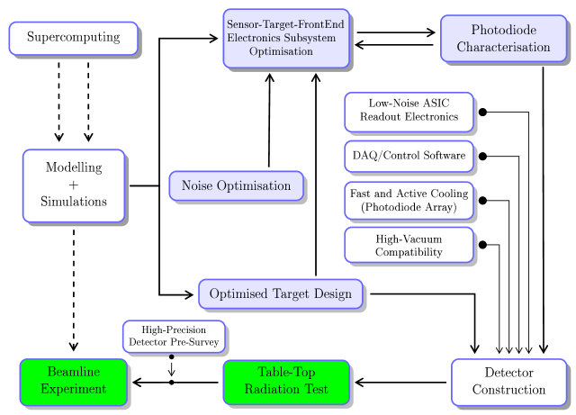
At the inception of this R&D project, a handful of design considerations were taken into account and thus led to building effectively functioning prototypes. The principal design goals pursued are listed in order of priority as follows: (1) submicron-scale sensitivity, (2) preservation of -ray beam properties, such as photon flux and relative energy spread (), on the downstream side of the detector, (3) ultralow-noise operation, (4) high-vacuum compatibility, and (5) compact and cost-effective design. As identified, these five considerations are foundational for the design of position-sensitive detectors that are highly efficient for detecting photonsgruner:xray_det . The model-based full optimisations, based on which the detector prototype was constructed, gave the design a boost to its photon-detection efficiency and enabled a resulting enhancement of signals. In support of the low-noise design, active and fast detector-cooling modules and a dedicated control system for photon-counting application were integrated en masse into the photon-detection system. Consequently, it was made possible to create a novel avenue towards a boost to detector’s signal-to-noise (SNR) ratio and a pathway of achieving its ultrahigh spatial sensitivity. Additionally, utilising the parametric optimisation method can empower detector designers to react nimbly to satisfy varying needs for individual beamline programs at light-source facilities. Illustrated as a whole in Fig. 1 is the codified process of prototyping a custom detector attaining the targeted sensitivity.
2 Results
Principle of operation
As illustrated in Fig. 2(a), the detector system design consists of four key functional components: (1) a ring array of Si(PIN) diodes serving as a multisegmented photosensor, (2) a thin metallized film as a source of fluorescence radiation, (3) its dedicated ASIC-based readout electronics, and (4) single-stage micro-thermoelectric (Peltier) coolers and a water-cooling module, all of which are interfaced with a copper heat sink, or heat exchanger. In essence, the sensor-target subsystems, surrounded by the readout electronics and cooling modules, are situated at the very heart of the detector system. Importantly, the thin fluorescing film–henceforth referred to as fluo-film, or fluo-target, or target for short–is introduced to the design in order to act as a source of secondary -ray radiation emitted upon impingement of primary -ray radiation. As an addition, a lead (Pb) scatter shield, or visor, is inserted immediately upstream from the sensor array, so as to safeguard the ultrasensitive photosensors against potential stray signals that may arise during operation. And both upstream and downstream beryllium windows on a multi-port vacuum chamber are designed to be thin enough in consideration for downstream photon-starving experiments.
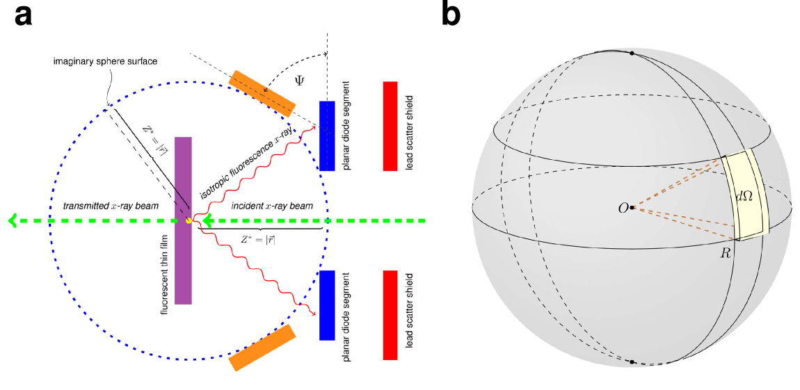
As depicted in Fig. 2(b), the effective beam-through apertures are set to accept, at least, a 5- footprint of an incident beam. The dimension of this central aperture accordingly limits the linear working range to a few millimetres for a highly focused nanometre-size beam, based on the 0.5-rad tolerance for the beam-pointing stability required by the National Synchrotron Light Source II (NSLS-II) facilitynsls2:cdr . Focused -ray beams are then guided to propagate unimpeded in a high vacuum, passing through the circular apertures on both the sensor ring and the scatter shield. Moreover, the fluorescing target is arranged in a configuration orthogonal to the propagating direction of incident -ray radiation. When primary radiation impinges upon the fluo-film, a paucity of -ray radiationserpell:xrf emanates in the backward direction in the form of characteristic -ray emission. As a result, the emission of nascent fluorescence radiation illuminates the backside of the sensor array. At the same time, the vast majority of incident photons are transmitted. In this process, the orthogonal beam-target topology becomes a critical factor for monitoring a monochromatised beam with ultrahigh precision. On this account, the orthogonal target configuration is required for the following three reasons: First, the normal incidence forces an incident beam to experience from beam’s vantage point an uniform effective thickness of each fluo-target, regardless of its point of incidence. Thus, the normal incidence of primary radiation on the target makes it possible to preserve the incident beam properties during the process of transmission and propagation towards a sample at the opposite end of the beamline from the light source. Second, the on-target normal incidence, in turn, ensures isotropic illumination and uniform photon detection over the entire active area of the planar sensor array. And third, during transmission of -ray beams through the thin film, scientists can derive its beam centroid from its entire beam profile, benefiting from uniform illumination over the diode array. On top of the orthogonal configuration, suppression of background-event signals is another critical issue. Taken all together, the backward-scattering mode of operation was favoured over the forward-scattering mode in the light of minimising potential systematic uncertainties arising during operation. The choice of the operation mode was borne out by the fact that the former mode can suppress elastically scattered photons (i.e., Rayleigh scatterings) coming from the target. Consequently, the sensor array captures backward-scattered fluorescent radiation with higher detection efficiency and spectral purity. Furthermore, three decisive advantages of using secondary -fluorescent radiation are the followingperujo:k_alpha : (1) distinctively high intensity and variable photon flux, (2) high spectral purity, and (3) the availability of a wide selection of fluo-film materials with reference to the energy of incident radiation.
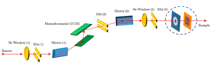
To visualise its full range of beamline operation, Fig. 3 shows a schematic setup for monochromatic beamline components and the -ray detector. One of the design features of note is that its compact lateral form factor ( 1 ft.) makes it possible for each beamline to accommodate multiple colocated detectors. This way a set of -ray detectors operational along a beamlne enables extracting more beam parameters, such as divergence angles, beam emittances, and so forth.
2.1 Photosensor design
As an optical receiver, the photodiode ring array is coupled with a fluo-target and its dedicated front-end readout circuitry, all of which take the form of the trio core subsystems. It is thus of foremost importance in designing a sensor ring array, that is most optimal for both the target and the readout electronics, and a photodetector with low-noise signal processing.
Achieving the targeted sensitivity level presents two main challenges to the design: (1) how to give rise to a substantial increase in photon-detection efficiency and (2) how to realise ultralow-noise photon-detection and operation under a high photon flux ( photons/s) environment. The two-track approach was correspondingly taken to rise to the said challenges: The first approach was to develop an effectual method of enhancing a higher degree of photon-detection efficiency, resulting in acquiring far more signals from the sensor array. Unlike the prior developments elsewherealkire:quad_bpm ; decker:pac2007 ; decker:biw2010 ; owen:pindiodes ; southworth:quad_pin_diode_xbpm , the sensor designs have the form of a multisegmented annular ring, covering the full range of 2-azimuthal angle, thus enabling highly efficient capture of isotropic fluorescent radiation (Fig. 4(a)–(d)). As the first step towards the photometric optimisation, calculations of solid angle bradt:astronomy , subtended by the diode ring array at a source of fluorescence radiation, were worked out by virtue of finding real-valued analytical functions (Eqs. (S1) and (S2)). Referring to Fig. 2(b), the four-parameter solid angles, subtended at a point source, are expressed by Eqs. (1a) and (1b). Here, and denote respectively a solid angle for the planar sensor and a solid angle projected onto the spherical surface for the curvilinear sensor.
| (1a) | |||
| (1b) | |||
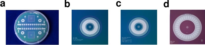
where the projection factor is defined as (Fig. 2(a)). The variables and represent respectively the working distance of the target from the sensor plane and the total number of diode segments in the array. And , , and signify polar angle, radial coordinate components of the sidelines of each diode segment, respectively (Supplementary Fig. 1). In the case of a planar sensor (Fig. 2(a)), the projection factor is put into play for calculating solid angles with precision. First and foremost, the application of this parametric method allows for quantitatively determining a practical range of working distance optimal for the target in use. As observed in Fig. 5(a), the optimised sensor array attains its total peak solid angle of 0.90 steradian, or integrated field of view of 3000 , under irradiation with photon beams having a 90-m diameter at an optimal working distance of 4.5 mm–the number of photon counts peaks out when target’s working distance is at this calculated optimum position. Given these parameters, the photon-detection efficiency of the optimised core subsystems is estimated to be . Ultimately, this parametric method provides a quantitative basis for determining the optimal layout and dimensions of the sensor array with the inclusion of multiple guard rings and the central aperture. The foregoing analytical model made it possible to perform a series of rigorous analyses for fine-tuning the optimisation of the core subsystem. According to the calculation results, two optimised versions were fabricated—dubbed Prototype-II-32 and Prototype-II-64— in reference to the unoptimised Prototype-I. As Fig. 4(b)–(d) shows, the total surface areas of Prototype-II were halved, whereas its peak solid angle and photon-detection efficiency doubled as a direct result of the photometric optimisation. In addition, the full optimisation, by including spatial constraints imposed by indirect-bandgap semiconductors, produced a compact design, thus creating enough room for multiple concentric-circular guard rings. Accordingly, a system of two inner and three outer guard rings was incorporated in order to smoothly step down the electric potential to the ground (Fig. 4(b) and (c)). As a side benefit, the resulting miniaturisation made its way for lower-cost and higher-volume manufacturability on a single wafer. And the second approach was the minimisations of the system-wide noise levels achieved in various ways. As part of the optimisation process, the idea of multisegmentation was introduced to the design of ring-shaped diodes. It was based on the fact that the multisegmented design offers a few benefits to recognise: In the first place, the multisegmentation allows for the reduction in junction capacitance, thereby suppressing series noise and enabling sensor’s faster response. In the second place, this multisegmentation provides the benefit of creating fine-tuning knobs for enabling capacitive matching between each diode segment and the front-end readout circuit. Upon sensor fabrication, full electrical characterisation was performed on individual diode segments. Follow-up extraction of the characteristic parameters in detail rendered quantification of detector’s performance, which was fed into the optimisation loop, as illustrated in Fig. 1.
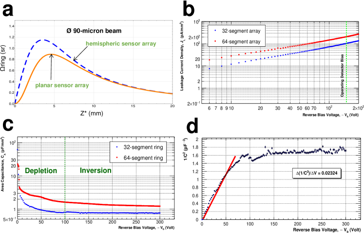
When irradiated with photon beams of 90- diameter, the total solid angle of the planar sensor array peaks at 4.5 mm, whereas an optimised hemispheric sensor array is expected to bring about a further increase of 30 in its solid angle (Fig. 5(a)). It was observed from Fig. 5(b) that surface leakage current density increases linearly with the reverse-biased voltage applied across the p-i-n junction with ohmic contacts. In particular, the – measurements took into account leakage currents as a dissipation factor (Fig. 5(c)). Furthermore, dopant concentration was obtained from the slope of the – curve in the depletion region (Fig. 5(d)). And it was ascertained from Fig. 5(b) that the level of leakage current density is held below 100 under reverse-biased DC sweep down to at room temperature, while satisfying a set of the design criteria. On the other hand, under the applied electric field, sensor capacitance decreases until full depletion is reached at around (Fig. 5(c)). In the inversion region, the areal capacitance as low as 0.5 pF was measured at the maximum depletion depth on 100 , based upon which the capacitive matching was conducted (Fig. 5(c))radeka:psd ; poc:cmos . Listed as a summary in Table 1 are salient detector parameters extracted from the – and – measurements. A silicon p-i-n (Si(PIN)) diode of high-speed response produces sufficiently low leakage currents even at room temperature without requiring a cryogenic cooling system. Moreover, a wide dynamic range and excellent linearity are inherent to the silicon material. Cognisant of these properties, silicon was opted over other semiconducting materials –e.g., Ge and Si(Li)–for the detection of hard/tender -ray radiation (2 25 keV). Notably, the sensor array operates as a double-side junction–the frontside (device side) and the backside (window side)-illuminated structurerehak:sdd ; carini:sdd .
| Parameters | Values |
|---|---|
| total sensor thickness, | 480 m |
| silicon oxide thickness, | 560 nm |
| depletion voltage, | 150 |
| depletion depth, | 200 m |
| leakage current density, | 0.12 [260 K] / 104 [300 K] |
| effective dopant concentration, | 5.0 |
| resistivity, | 1.0 - |
| extrinsic Debye length, | 1.85 m |
| junction capacitance, | 0.5 |
| shunt resistance, | 180 |
| carrier transit time, | 10.2 []/34.1 [] |
| rise time response, | 1.9 |
| RC time constant, | 0.9 |
| time resolution, | 2.8 |
| bandwidth, | 180 |
| noise equivalent power ( = 229 nm) | 1.6 |
| specific detectivity, | 6.4 |
2.2 Thin fluorescing film.
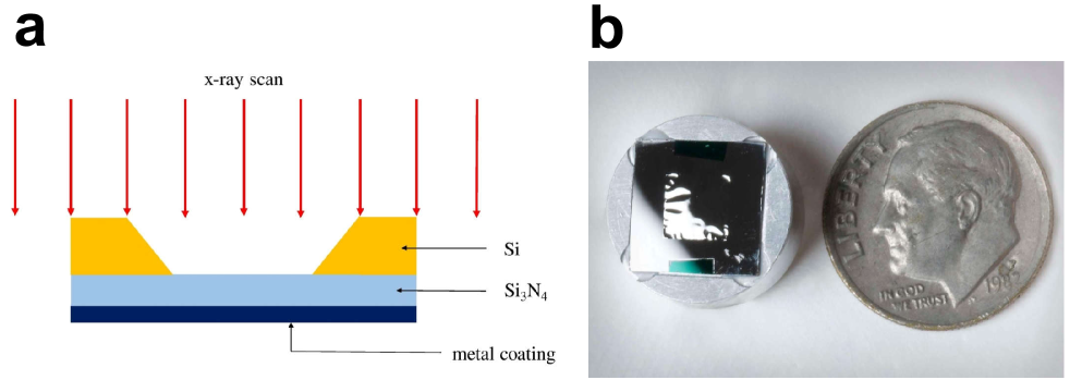
A high-transmission fluo-film optimal for the incident beam energy was constructed with the identification of the following elements to consider: (1) the range of the energy of the -ray beam in operation, (2) the optimal range of beam energy to which the detector responds, (3) K-shell absorption edge of the fluorescing target material, and (4) the intensity expected in the -ray beam. A priori information described above sets standards for selecting appropriate film materials. Hence, the selection of materials becomes a necessity, based on their K-shell values having sufficient separation below the energy of incident -ray beams. The following is a list of the selection along with respective values of and wavelength : \BPChem_22Ti ( = 4.511 keV; = 2.749 ), \BPChem_24Cr ( = 5.415 keV; = 2.290 ), \BPChem_25Mn ( = 5.899 keV; = 2.102 ), \BPChem_26Fe ( = 6.404 keV; = 1.936 ), \BPChem_27Co ( = 6.930 keV; = 1.789 ). The -ray transmission efficiency and fluorescence signals contend with each other. The optimal thickness of each of the film materials was determined from the existing experimental data of mass-absorption coefficients from the literature hubbell:survey ; hubbell:photon_mass_atten_coeff ; alkire:mass_absorp_coeff and numerical simulations that follow (Supplementary Fig. 2). In such a way, transmission rates of incident photon energy of 8-keV are above 90 with a selection of differing metallic media for use as a thin film. The transmission efficiency of an incident -ray beam is important particularly for photon-starving experiments being conducted at synchrotron light sources. The thickness of thin metal film is often too feeble to enable a self-supporting fluo-target of adequate quality. As a solution, a robust -ray transmission window was introduced to the fluo-film design. The substrate material of choice is the commercial silicon nitride () window (Norcada, Inc., Edmonton, AB, Canada: NX10500E, Supplementary Fig. 3), which is known to be a low-stress ( 250 MPa) radiation-hard substrate for -ray applicationsgw:si3n4 ; toermae . For providing sufficient mechanical strength, a 500-nm thick single-layered film was vacuum-sputtered through a mask onto the silicon-nitride window (5 mm 5 mm 500 nm) at the NSLS-II in-house facilityconley:multilayer . Displayed in Fig. 6 (a) and (b) are the structure of the -ray window and a thin film supported by the window substrate mounted onto an aluminium placeholder.
2.3 Photon-transport Monte-Carlo simulations
During detector operation, background signals from coherent elastic and incoherent inelastic scattering may be emitted anisotropically in addition to fluorescent signals, owing to the polarisation of synchrotron radiation in the plane of synchrotronlandau:synchrad ; schwinger:synchrad . For the quantitative assessment of signals and backgrounds, Monte-Carlo (MC) simulation techniques were employed to study -ray absorption, scattering, and fluorescent radiation. Relying on the use of EGS4-based RÖntgen SImulator (RÖSI version 0.19) packagerosi ; namito:egs4 , the MC simulations were conducted with the inclusion of the geometry of the entire detector assembly and the vacuum chamber. Detector simulations, using realistic statistics of photon flux ( photons/s), were carried out on high-performance supercomputing platformsnersc . The primary purposes of such high-fidelity MC simulations are the following: (1) quantification analysis of detector performance and (2) estimation of potential background events coming from ambient scatterings, both of which are important for attaining its submicron-scale sensitivity. This MC model collectively included signals from -ray fluorescence and Rayleigh and Compton scatterings. In particular, the angular distribution of Rayleigh photons of a few keV, which are scattered from medium- or high-Z materials, is confined mostly in a wide-angle cone open in the forward directionklein_nishina ; nelms_oppenheim . For the photon energy ranging from 10 to 50 keV, the photoelectric interaction is the dominant signal process, having sole responsibility for the fluorescence phenomenon. On the other hand, Rayleigh scattering is the dominant background process over Compton scattering in the energy range of 5 25 keV. With the selection of materials (i.e., \BPChem_24Cr, \BPChem_25Mn, \BPChem_26Fe, and \BPChem_27Co), MC studies show that estimated contributions from the two competing interactions –Rayleigh and Compton scatters–are as insubstantial as below the level of 1.0 and 0.1 , respectively. As defined in equation (2), the photon purity of the K-shell fluorescent radiation is the ratio of K-shell fluorescent radiation to a sum of scattered radiation and :
| (2) |
Further, the MC simulations indicated that the purity for each individual element in the selection amounts to nearly 100 in a vacuum.
2.4 Readout electronics and peripheries
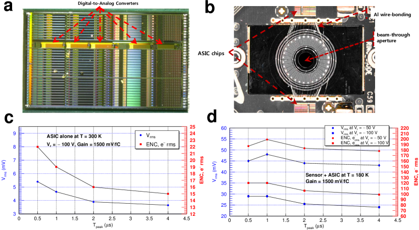
Compact in-vacuum readout electronics were designed, utilising dedicated application-specific integrated circuits (ASICs) for the high-rate photon-counting application. The HERMES4 ASIC, based upon 350-nm CMOS technology, offers 32 channels of low-noise charge amplification, high-order shaping with baseline stabilisation, and peak detection for various low-noise analogue/digital processing (Fig. 7(a))degeronimo ; cook:czt . For reducing stray capacitance and for suppressing signals stemming from electrical interconnections, each sensor segment in the array is wire-bonded directly to the input of the front-end readout channel (Fig. 7(b)). As such, Al-wire wedge bonding and the ultrasonic technique were utilised between the input of an ASIC channel and a bonding pad implemented on each diode segment. According to the measurements, ASIC noise optimisation enables an electronic resolution of 15 rms (equivalent noise charge, or ENC) with a choice of 4-s peaking time at room temperature. With multisegmented photosensor’s high finesse, the event rate per each ASIC channel is diminished to 40 kHz in a high-flux SR condition. As a result, the front-end readout with low-power consumption (8 mW/channel) was realised. For high-flux applications, one major challenge is how to design associated readout electronics capable of processing sufficiently high photon statistics without reaching charge saturation. It was observed during a beamline experiment that the processing rate of this ASIC readout chip can cope with 100 kHz per channel. Additionally, the integrated cooling subsystem functions to lower the operating temperature of the Si(PIN)-diode array nestled on the readout printed circuit board. Hence, the active and fast detector cooling is an added functional feature that helps minimise persistent system-wide parallel noise. In this respect, the detector system is outfitted with efficient cooling modules in three ways: (1) A ring array of thermoelectrically-cooled diodes is included in the power budget for minimising bulk leakage currents. (2) Both the readout electronics and the thin film make exceptionally good thermal contact with a water-cooled heat sink copper block. And, (3) applying adhesive with high thermal conductivity (5.77 W/m K) for interconnecting individual components yields a remarkable enhancement of the heat-transfer process. As a consequence, its operating temperature can plummet to in as fast as a few seconds after power-up. As an integral component of the detector system, the mechanical support made of an Invar 36 (Alloy 36)patent:invar was designed together. This instrument support system of high thermal stability (100 nm//hr) ensures the steady maintenance of detector’s high-precision alignment and spatial sensitivity in a temperature-controlled environment throughout each year.
2.5 Radiation experimentation
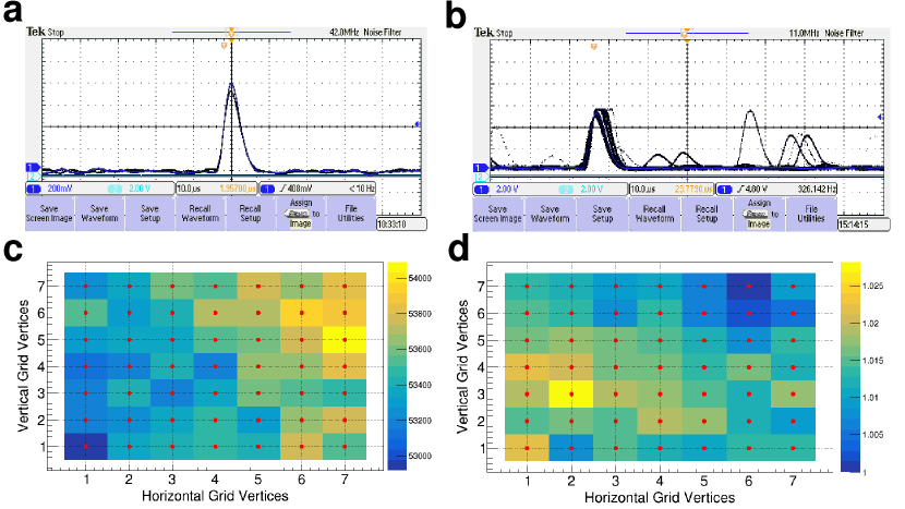
As a proof of concept, a table-top experiment was carried out first at room temperature with an Fe-55 sealed radioactive source, confirming the acquisition of noise-free detector response (Fig. 8 (a)). Next, the prototype detector, loaded with the fully optimised 32-segment sensor (Prototype-II-32) and target, was experimented with polychromatic beams at the X7A beamline of the National Synchrotron Light Source. Prior to the SR experiment, high-precision alignment ( 60 ) of the detector assembly was ensured at the beamline in an effort to minimise systematic uncertainties. The amount of detector noise, intrinsic to the radiation sensor and the front-end readout system, was minimised consistently during both the table-top and the SR beamline experiment. As evidenced by the experimental observations, the noise floor was brought down to the bottom level at in high-vacuum conditions (Fig. 8(a) and (b)). Then, a subsequent SR experiment was dedicated to one full round of beam-based transverse aperture scan with -ray beams of 90 in diameter in regular steps of 600 nanometres (nm) over 7 7 mesh grid. As cogent evidences, the variations of photon counts from each channel are mapped to the colour scales on the right-hand column and projected over the mesh grid (Fig. 8(c) and (d)). This way the mesh plots visualise the variations of photon counts at each of the 49 vertices with the submicron interval. Hence, these colour maps clearly delineate that the detector design has its capability to respond with 600-nm sensitivity and better under intense irradiation of -ray photon beams at the given energy.
3 Discussion
Leveraging the systematic design method, developed for fully optimising the detector system and for eliminating noise sources, maximised its SNR and thus boosted its spatial sensitivity. Consequently, the long-standing barrier of detector’s submicron sensitivity has been broken down. This breakthrough was achieved by amalgamating technologies from manifold areas of research fields. Eventually, the custom-design method, offering great flexibility to add more new ideas and features, became a product of the transdisciplinary approach, thereby ushering in the realm of nanometre-range sensitivity. In a conventional prototyping process, a significant amount of lead time and cost is needed for completing an entire detector prototyping process. By contrast, taking the two-prong approach reported in this Article makes it possible to design an archetype of the photodetector reaching a desired level of sensitivity at a fraction of the previously required time and cost. Above all, the detector design, ensuring normal incidence of primary radiation, is apposite particularly to highly focused monochromatised -ray beams, expecting its surpassing photometric performance. Further enhancements of its detection efficiency and sensitivity will involve optimising the sensor-target subsystem based on a beam dimension and developing hemispheric, or semi-hermetic 2-photodetectors open in the forward direction. The calculations in Fig. 5(a) also corroborate the concave photodetector systems designed elsewhereko:eye_camera ; someya:eyeball . Hence, one practicable solution to suggest is building such an optimised concave photodetector in a honeycombed structure. The benefits from utilising such ultrahigh-precision instruments are expected to ripple out across the scientific community. Further, the position-sensitive detector of fluorescence type, realised by the tailored design process, has a likely impact on applications of wide and far-reaching appeal to the scientific and industrial research alike.
References
- [1] R. W. Alkire, G. Rosenbaum, and G. Evans. Design of a vacuum-compatible high-precision monochromatic beam-position monitor for use with synchrotron radiation from 5 to 25 keV. J. Synchrotron Rad., 7:61–68, 2000.
- [2] G. P. Decker, Den Hartog, O. Singh, and G. Rosenbaum. Progress toward a hard X-ray insertion device beam position monitor at the advanced photon source. Proc. of Particle Accelerator Conference (PAC) 2007, Albuquerque, New Mexico, USA., 2007.
- [3] G. Decker, B. X. Yang, R. Lill, and H. Bui. APS Beam Stability Studies at the 100-Nanoradian Level. Proc. of Beam Instrumentation Workshop (BIW) 2010, Santa Fe, New Mexico, USA., 2010.
- [4] R. L. Owen, J. M. Holton, C. Schulze-Briese, and E. F. Garman. Determination of X-ray flux using silicon pin diodes. J. Synchrotron Rad., 16:143–151, 2009.
- [5] S. H. Southworth and P. L. Cowan. X-ray beam position monitor using a quadrant PIN diode. Nucl. Instrum. Methods Phys. Res., Sect. A, 319:51–55, 1992.
- [6] C. J. Kenney et al. Use of active-edge silicon detectors as X-ray beam monitors. Nucl. Instrum. Methods Phys. Res., Sect. A, 582:171–181, 2007.
- [7] R. Plankett et al. X-ray metrology of an array of active edge pixel sensors for use at synchrotron light sources. Nucl. Instrum. Methods Phys. Res., Sect. A, 879:106–111, 2018.
- [8] A. D. Carg et al. Design of -ray diagnostic beam line for a synchrotron radiation source and measurement results. Nucl. Instrum. Methods Phys. Res., Sect. A, 754:15–23, 2014.
- [9] Brookhaven’s Next Big Machine, NSLS-II, makes progress. J. Synchrotron Rad., 16:693–694, 2009.
- [10] NSLS II Conceptual Design Report. BNL-77977-2006-V1-V2, 2006.
- [11] C. J. Serpell et al. Carbon nanotubes allow capture of krypton, barium and lead for multichannel biological -ray fluorescence imaging. Nat. Commun., 7:13118, 2016.
- [12] M. Kinebuchi et al. Diagnostic copper imaging of Menkes disease by synchrotron radiation-generated X-ray fluorescence analysis. Sci. Rep., 6:33247, 2016.
- [13] S. M. Gruner, E. F. Eikenberry, and M. W. Tate. X-ray Detectors. International Tables for Crystallography, Crystallography of biological macromolecules, Springer Netherlands, F:143–147, 2006.
- [14] A. Perujo et al. Deviation of the / intensity ratio from theory observed in proton-induced -ray spectra in the 22 Z 32 region. J. Phys. B: At. Mol. Phys. 20 4973, 20:4973, 1987.
- [15] H. Bradt. Astronomy Methods: A Physical Approach to Astronomical Observations, 1 edn., chapter 3, pages 45–47. Cambridge University Press, Cambridge, UK, 2004.
- [16] V. Radeka. Semiconductor Position-Sensitive Detectors. Nucl. Instrum. Methods Phys. Res., 226:209–218, 1984.
- [17] P. O’Connor and G. De Geronimo. Prospects for charge sensitive amplifiers in scaled CMOS. Nucl. Instrum. Methods Phys. Res., Sect. A., 480:713–725, 2002.
- [18] P. Rehak et al. Arrays of silicon drift detectors for an extraterrestrial X-ray spectrometer. Nucl. Instrum. Methods Phys. Res., Sect. A., 624:260–264, 2010.
- [19] A. G. Carini et al. Performance of a Thin-Window Silicon Drift Detector X-ray Fluorescence Spectrometer. IEEE Trans. Nucl. Sci., 56:2843–2849, 2009.
- [20] J. H. Hubbell. Survey of Photon-Attenuation-Coefficient Measurements 10 eV to 100 GeV. Atomic Data, 3:241–297, 1971.
- [21] J. H. Hubbell. Photon Mass Attenuation and Energy-absorption Coefficients from 1 keV to 200 MeV. Int. J. Appl. Radiat. Isot., 33:1269–1290, 1982.
- [22] R. W. Alkire. Approximating the near-edge mass absorption coefficients for Ni using an ultra-thin bimetal foil. J. Appl. Cryst., 50:1–13, 2017.
- [23] J. Steinlechner et al. Optical absorption of silicon nitride membranes at 1064 nm and at 1550 nm. Phys. Rev. D, 96:022007, 2017.
- [24] P. T. Törmä et al. Ultra-Thin Silicon Nitride X-ray Windows. IEEE Trans. Nucl. Sci., 60:1311–1314, 2013.
- [25] R. Conley et al. The NSLS-II Multilayer Laue Lens Depositon System. Proc. of SPIE, 7448:74480U–1, 2009.
- [26] L. Landau and E. Lifschitz. The Classical Theory of Fields, 3 edn., chapter 74, pages 197–202. Pergamon Press Ltd., Oxford, UK, 1971.
- [27] J. Schwinger. On the Classical Radiation of Accelerated Electrons. Phys. Rev., 75:1249, 1949.
- [28] J. Giersch, A. Weidemann, and G. Anton. ROSI–an object-oriented and parallel-computing Monte Carlo simulation for -ray imaging. Nucl. Instrum. Methods Phys. Res., Sect. A., 509:151–156, 2003.
- [29] Y. Namito, H. Hirayama, and S. Ban. Improvements of low-energy photon transport in EGS4. Radiation Physics and Chemistry, 53:283–294, 1998.
- [30] W. E. Johnstone. Computational and data grids in large-scale science and engineering. Future Generation Computer Systems, 18:1085–1100, 2002.
- [31] O. Klein and Y. Nishina. Über die Streuung von Strahlung duruch freie Elektronen nach der neuen relativistischen Quantendynamik von Dirac. Zeitschrift für Physik, 52:853–868, 1929.
- [32] A. T. Nelms and I. Oppenheim. Data on the Atomic Factor: Computation and Survey. J. Res. Nat. Bur. Stds., 55:53–63, 1955.
- [33] G. De Geronimo et al. ASIC With Multiple Energy Discrimination for High-Rate Photon Counting Applications. IEEE Trans. Nucl. Sci.,, 54(2):303–312, 2007.
- [34] W. R. Cook, J. A. Burnham, and F. A. Harrison. Low-noise custom VLSI for CdZnTe pixel detectors. Proc. of SPIE: SPIE Conference on EUV, X-Ray, and Gamma-Ray Instrumentation for Astronomy IX,, 3445:347–354, 1998.
- [35] W. M. Sokolowski, M. S. Lane, C. H. Hsieh, and T. P. O’Donnell. Ultrahigh-purity dimensionally stable INVAR 36, 12 1995.
- [36] H. C. Ko et al. A hemispherical electronic eye camera based on compressible silicon optoelectronics. Nature, 454:748–753, 2008.
- [37] T. Someya. Optics: Electronic Eyeballs. Nature, 454:703–704, 2008.
4 Acknowledgements
This R&D work was conducted under the aegis of the U.S. Department of Energy, Office of Basic Energy Sciences, by Brookhaven National Laboratory (BNL) under contract number DE-AC02-98CH10886. The author acknowledges the provisions and arrangements made by the detector development group and the beamline support group of National Synchrotron Light Source-II, and the Instrumentation Division of BNL throughout.