High thermoelectric efficiency in monolayer PbI2 from 300 K to 900 K
Abstract
By using a first-principles approach, monolayer PbI2 is found to have great potential in thermoelectric applications. The linear Boltzmann transport equation is applied to obtain the perturbation to the electron distribution by different scattering mechanisms. The mobility is mainly limited by the deformation-potential interaction with long-wavelength acoustic vibrations at low carrier concentrations. At high concentrations, ionized impurity scattering becomes stronger. The electrical conductivity and Seebeck coefficient are calculated accurately over various ranges of temperature and carrier concentration. The lattice thermal conductivity of PbI2, 0.065 W/mK at 300 K, is the lowest among other 2D thermoelectric materials. Such ultralow thermal conductivity is attributed to large atomic mass, weak interatomic bonding, strong anharmonicity, and localized vibrations in which the vast majority of heat is trapped. These electrical and phonon transport properties enable high thermoelectric figure of merit over 1 for both p-type and n-type doping from 300 K to 900 K. A maximum of 4.9 is achieved at 900 K with an electron concentration of 1.91012 cm-2. Our work shows exceptionally good thermoelectric energy conversion efficiency in monolayer PbI2, which can be integrated to the existing photovoltaic devices.
Organic-inorganic CH3NH3PbI3 perovskite solar cells have emerged as a leading next-generation photovoltaic technology Kojima et al. (2009); Lee et al. (2012); Park (2013); Snaith (2013); Kim et al. (2014); Habisreutinger et al. (2014); Green et al. (2014); Service (2014); Hodes and Cahen (2014); Lin et al. (2015). As the precursor material used to fabricate perovskite thin films Burschka et al. (2013); Jeng et al. (2013); Ng et al. (2015); Fu et al. (2015); Hill et al. (2015); Bae et al. (2016); Yi et al. (2016); Zhu et al. (2016); Raga et al. (2016); Noel et al. (2017), lead iodide (PbI2) leads to remarkable advances in efficiency due to the 6 electronic configuration of Pb Ganose et al. (2016). Encapsulated perovskite devices with excess PbI2 exhibit good stability Liu et al. (2016). An excess of PbI2 is beneficial to a better crystallization of the perovskite layer and improves the performance of perovskite solar cells Duong et al. (2016); Bi et al. (2016); Wang et al. (2016a); Kim et al. (2016). After long exposures, CH3NH3PbI3 eventually forms PbI2 due to its instability in moist air Christians et al. (2015); Chen et al. (2014a); Leguy et al. (2015); Yang et al. (2016a, 2015). According to this degradation process, waste PbI2 at the end of its useful life can be recycled using an appropriate solvent Chen et al. (2014b); Babayigit et al. (2016). Therefore, although CH3NH3PbI3 perovskite has a drawback in the toxicity of lead Smith et al. (2014); Savory et al. (2016); Gupta et al. (2016), the perovskite technology can be deployed in a completely safe way by recycling PbI2.
After absorbing solar energy, the photo-induced carriers are generated in the CH3NH3PbI3 region, while the PbI2 passivation layers can prevent back recombination and facilitate charge separation Shih et al. (2017). Besides the sunlight collected by the perovskite solar cells, a large fraction of solar energy is converted into heat in the form of phonons as well He and Galli (2014). Such heat can be converted into electricity by thermoelectric materials when the temperature gradient is generated. Here we show for the first time that PbI2 itself is a promising candidate for high-efficiency thermoelectric applications.
The fabrication of PbI2 nanostructures is being pursued with increasing interest in chemistry, physics, and material science Sandroff et al. (1986); Tan and Wright (1987); Kasi et al. (2007); Baltog et al. (2009); Cabana et al. (2014); Zhong et al. (2016); Wang et al. (2016b); Zheng et al. (2016); Frisenda et al. (2017); Zhong et al. (2017); Wang et al. (2017). In this work, we focus on monolayer PbI2 only, because of the following reasons: (1) Evidence for the reversible formation of monolayer PbI2 has been found in 1987, which discovered that a monolayer precedes the production of bulk PbI2 Tan and Wright (1987). By using cyclic voltammetry to study the electrocrystallisation of PbI2, the monolayer is found to appear at an underpotential of -65 mV with respect to the reversible potential of crystalline PbI2, and this can be explained by the reduction of surface tension which occurs when the solid electrode is covered by a monolayer. Under such laboratory conditions, monolayer PbI2 is more stable than bulk PbI2 by -13 kJ/ Tan and Wright (1987). (2) Bulk PbI2 usually has a rough surface as well as lots of defects, which strongly reduce the carriers mobility Zhang et al. (2015), while in 2D PbI2, low-density defects and ultrasmooth surface have been observed Zheng et al. (2016). (3) Low dimensionality provides a effective conductive channel for carriers and reduces phonon thermal transport at the same time Arab and Li (2015). (4) Most interestingly, it is possible to fabricate PbI2 with other 2D materials by layer-engineering in photovoltaic and thermoelectric systems Zhou et al. (2015). Thus monolayer PbI2 is preferred for its transparency.
| Carrier type | () | (eV) | (J/m2) | (cm2/Vs) | (cm2/Vs) | ( cm2/Vs) |
|---|---|---|---|---|---|---|
| hole | 17.33 | -1.79 | 14.36 | 1.94 | 1.95 | 3.66 |
| electron | 0.73 | -4.41 | 14.39 | 69.52 | 81.66 | 21.73 |
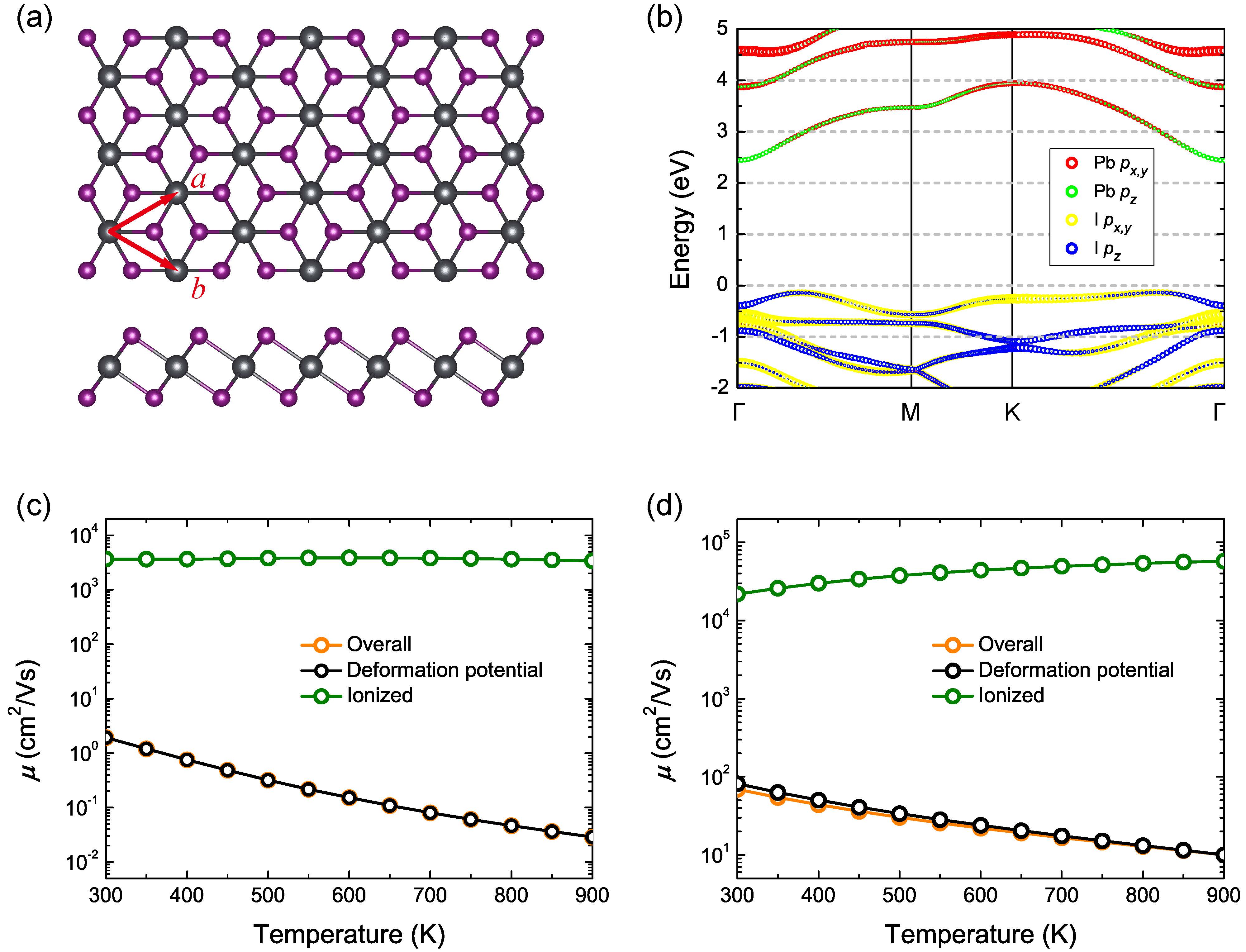
Monolayer PbI2 crystallizes in the space group . The optimized lattice constant of 4.66 Å and height of 3.73 Å are in good agreement with previous results Zhou et al. (2015); Lu et al. (2016). Each Pb atom is octahedrally surrounded by six I atoms, and I atoms themselves are hexagonally close packed, as shown in Figure 1(a).
We now turn to study the electronic structures and carrier mobility of monolayer PbI2. The band structure is calculated using the HSE functional with spin-orbit coupling, as shown in Figure 1(b). The calculated band gap is 2.57 eV, reproducing well the previous theoretical and experimental results Zhou et al. (2015); Zheng et al. (2016). The conduction band minimum (CBM) is located at point, while the valence band maximum (VBM) shifts a little away from point. The VBM (CBM) bands mainly result from I- (Pb-) states.
Both elastic (ionized impurity, piezoelectric, and deformation potential interaction) and inelastic (polar optical phonons) scattering mechanisms are taken into account in calculating the mobility Faghaninia et al. (2015). The dielectric measurements show that for PbI2, =6.25 Dugan and Henisch (1967). Thus the electron-polar optical phonon scattering rates, , are much lower than elastic scattering rates. It should be noticed that the and are measured on bulk PbI2. For monolayer PbI2, the low dimension reduces electronic screening, typically leading to smaller dielectric function. However, accurate estimation of dielectric function of monolayer PbI2 requires many-body perturbation theory Peng et al. (2018a). Here for simplicity we use the bulk value, and under such approximation, the electron-polar optical phonon scattering is negligible.
The total elastic scattering rate can be calculated according to Matthiessen’s rule Faghaninia et al. (2015)
| (1) |
where , , , and stand for elastic, deformation potential, ionized impurity, and piezoelectric scattering rates, respectively. Table 1 lists the related ab initio parameters for calculating the elastic scattering rates using the single-band approximation, as well as the overall mobility and the mobility limited by deformation potential and ionized impurity scattering with a carrier concentration of 1.9 cm-2 at 300 K.
The calculated mobilities from different scattering mechanisms are shown in Figure 1(c) and (d) for both p-type and n-type doping. Although it might be very difficult for n-type doping as monolayer PbI2 has a large band gap, it can be realized by electrostatic gating Li et al. (2016). By changing the gate voltage, the injected charge can be tuned Sun et al. (2018). With a zero piezoelectric coefficient , monolayer PbI2 does not exhibit pronounced piezoelectricity. This is because monolayer PbI2 has inversion center, as been observed in the 1T structure of SnS2 Blonsky et al. (2015). For comparison, monolayer MoS2, which has 2H structure and hence breaks inversion symmetry, shows a piezoelectric coefficient of 362 pC/m Blonsky et al. (2015). Thus the mobility cannot be limited by piezoelectric scattering.
For both p-type and n-type PbI2 with a carrier concentration of 1.9 cm-2, the mobility at 300 K is mainly limited by deformation potential interaction with acoustic phonons. At low carrier concentrations, the wavelength of thermally activated carriers is much larger than the lattice constant. Therefore the carrier mobility is determined by acoustic vibrational modes Bardeen and Shockley (1950); Xue et al. (2016). In deformation potential interaction, due to much smaller effective mass at the CBM, the electron mobility is much larger than hole mobility.
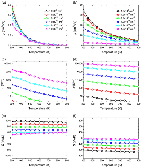
To determine the transport properties, we use the rigid band approximation, in which the electronic structure is unchanged with doping and only the Fermi level is shifted appropriately. For impurity doping, ionized impurities become scatterer centers and their concentration can be calculated at a given carrier concentration by iteratively solving the charge balance equation Faghaninia et al. (2015). Figure 2(a) and (b) show the calculated . With increasing carrier concentration, the ionized impurity scattering becomes stronger, which further reduces the carrier mobility.
Once is calculated, the electrical conductivity can be obtained at a given carrier concentration (assuming that the carrier concentration remains constant at different temperatures). As shown in Figure 2(c) and (d), the increases with increasing carrier concentration and decreases with increasing temperature.
The Seebeck coefficient measures the electrical potential difference created from a temperature gradient. As shown in Figure 2(e) and (f), the absolute values of are larger than 400 V/K at low carrier concentrations over a large range of temperature, which is larger than those of antimonene Peng et al. (2018b). At a hole concentration of 1.9 cm-2, the reaches nearly 1200 V/K. The absolute values of decrease with increasing carrier concentration. It should be noticed that, although the constant relaxation time approximation correctly predicts the trend in Seebeck coefficient with varying carrier concentration Madsen and Singh (2006), the predicted values are far from the experimental results because the treatment of relaxation time as a single constant affects both and when integrated over energy.
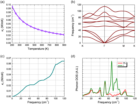
The key and remarkable feature of monolayer PbI2 is ultralow lattice thermal conductivity , which ranges from 0.096 W/mK at 200 K to 0.022 W/mK at 900 K. This extraordinarily low is much lower than other 2D thermoelectric material Wang et al. (2015, 2013); Sevincli and Sevik (2014); Tan et al. (2015); Lv et al. (2016); Peng et al. (2018b). To quantitatively understand the origin of ultralow in monolayer PbI2, we compare the results using the Boltzmann transport equation for phonons in Figure 3(a) with the Slack model Slack (1973).
According to the Slack model, the is given by Yang et al. (2016b)
| (2) |
where is the average mass, is the Debye temperature, and is the area per atom, is the Grüneisen parameters, is a related parameter Julian (1965), and is the number of atoms in the unit cell.
The calculated of 0.070 W/mK is close to that using the Boltzmann transport equation for phonons (0.065 W/mK). The Slack model attempts to normalize the effect of crystal structure, atomic mass, interatomic bonding, and anharmonicity. Monolayer PbI2 has a large atomic mass of 461 amu, while a low Young’s modulus of 13.61 N/m indicates weak interatomic bonding. Large atomic mass and weak interatomic bonding lead to a low Debye temperature of 123 K. In addition, as shown in Figure S1 in the Supporting Information, the mode Grüneisen parameters of PbI2 are comparable to those of state-of-the-art thermoelectric materials such as PbTe and SnTe Lee et al. (2014). Strong anharmonicity indicates strong three-phonon scattering strength Peng et al. (2016a), which is the dominant scattering mechanism in phonon transport of monolayer PbI2. Therefore, although monolayer PbI2 and monolayer ZrS2 have same crystal structure, due to large atomic mass, weak interatomic bonding and strong anharmonicity, the of PbI2 is much lower than that of ZrS2 (3.29 W/mK at 300 K Lv et al. (2016)).
To further understand the origin of ultralow thermal conductivity in PbI2, we examine the phonon vibrational properties. The calculated phonon dispersion is shown in Figure 3(b). The highest phonon frequency of monolayer PbI2 is 114.6 cm-1, which is lower than that of state-of-the-art thermoelectric material PbTe Tian et al. (2012) and Bi2Te3 Qiu and Ruan (2009), resulting in low phonon group velocity. Phonons with small group velocities are not effective carriers of heat Feldman et al. (1993).
In addition, as shown in Figure 3(d), the flattened dispersions, corresponding to the peaks of phonon density of states from 40 cm-1 to 80 cm-1, imply localized phonon vibrations. It is well known that the flat modes tend to increase the number of three-phonon scattering channels Li and Mingo (2015); Peng et al. (2016a). Besides increased scattering channels, localized phonon states also result in reductions in the group velocities. As a result, the vast majority of heat is trapped in flat, low velocity modes, as shown in Figure 3(c). Therefore phonons with frequencies from 40 cm-1 to 80 cm-1 contributes far less than those below 40 cm-1 or beyond 80 cm-1.
Generally, high thermoelectric performance is found in materials with high Seebeck coefficient , high electrical conductivity , and low thermal conductivity , and the efficiency is determined by the dimensionless figure of merit Zeier et al. (2016); Yang et al. (2016b)
| (3) |
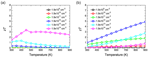
where is thermal conductivity consisting of electronic and lattice contributions. The electronic thermal conductivity relates to the electrical conductivity via the Wiedemann-Franz law , where is the Lorenz number Peng et al. (2016b). Combining electrical and phonon transport properties, the thermoelectric figure of merit in monolayer PbI2 is evaluated in Figure 4.
The highest reaches 4.9 at 900 K with an electron concentration of 1.91012 cm-2. Due to ultralarge Seebeck coefficient and ultralow thermal conductivity, high values over 1 are achieved in a wide temperature range from 300 K to 900 K, while most thermoelectric materials appear promising only at mid or high temperatures Zhao et al. (2014); Lin et al. (2016); Ying et al. (2016). Even for BiCu0.7Ag0.3SeO, the maximum at 300 K is only 0.07, while PbI2 reaches a of 1, distinguishing itself for low temperature thermoelectric applications. Moreover, PbI2 has been fabricated with perovskite thin film. It is tempting to build an additional PbI2-based thermoelectric device to harvest the heat produced by perovskite-based photovoltaic devices.
To conclude, we show that PbI2 is a promising thermoelectric material in a wide temperature range. By considering both the elastic and inelastic scattering mechanisms, highly accurate electrical transport properties are calculated using the linear Boltzmann transport equation. The acoustic-phonon limited mobilities at 300 K are 1.94 and 69.52 cm2/Vs for p-type and n-type doping at a carrier concentration of 1.9 cm-2, respectively. Large Seebeck coefficients are observed over large ranges of temperature and carrier concentration. Monolayer PbI2 exibits an ultralow lattice thermal conductivity of 0.065 W/mK at 300 K. The origin of the intrinsically low lattice thermal conductivity is due to large atomic mass, weak interatomic bonding and strong anharmonicity. Lattice dynamics calculations show that weak bonding interactions lead to localized vibrations, and consequently the vast majority of heat is trapped in these modes due to increased scattering channels and reduced group velocities. By integrating all these features, both p-type and n-type monolayer PbI2 exhibits a over 1 from 300 K to 900 K at certain carrier concentrations, enabling flexible applications in thermoelectrics. In particular, we achieve a maximum of 4.9 at 900 K with an electron concentration of 1.91012 cm-2. Considering lead iodide perovskites are widely employed in solar cells recently, it is possible to fabricate PbI2 with perovskite thin film in a hybrid thermoelectric and photovoltaic system, which may open up a path to a sustainable energy future. Experimental investigations are called for to verify our predictions and realize such devices in an industrially feasible way.
Methods
First principles calculations are performed using the Vienna ab-initio simulation package (VASP) based on density functional theory (DFT) Kresse and Furthmüller (1996). The generalized gradient approximation (GGA) in the Perdew-Burke-Ernzerhof (PBE) parametrization for the exchange-correlation functional is used. A plane-wave basis set is employed with kinetic energy cutoff of 600 eV. We use the projector-augmented-wave (PAW) potential with 5d electrons of Pb described as valence. A 15151 k-mesh is used during structural relaxation for the unit cell until the energy differences are converged within 10-8 eV, with a Hellman-Feynman force convergence threshold of 10-6 eV/Å. We maintain the interlayer vacuum spacing larger than 15 Å to eliminate interactions between adjacent layers.
Hybrid functional methods based on the Heyd-Scuseria-Ernzerhof method are also adopted Heyd et al. (2003, 2006); Peralta et al. (2006) with a 11111 k-mesh. The Wannier functions are generated for generic band interpolation with a 31311 k-mesh Mostofi et al. (2014). The electrical transport properties are in-plane isotropic and can be calculated using the Boltzmann transport equation Faghaninia et al. (2015). The band structure, density of state, electron group velocity, valence and conduction band wave function admixture, deformation-potential constant, 2D modulus, and polar optical phonon frequency are used in calculating the mobility. Based on the deformation potential theory in 2D materials Bruzzone and Fiori (2011); Xi et al. (2012); Cai et al. (2014); Qiao et al. (2014); Dai and Zeng (2015), we calculate the 2D elastic modulus and the deformation potential constant from the total energy and the positions of CBM and VBM with respect to the lattice dilation up to 1.5%. In calculating the piezoelectric constant Rode (1975), the elastic tensor including ionic relaxations is calculated using the finite differences method Le Page and Saxe (2002); Wu et al. (2005); Peng et al. (2017a), and the piezoelectric tensor is calculated using density functional perturbation theory (DFPT) Wu et al. (2005). Because the electrons are confined in 2D, the in-plane mobility is 3/2 the average mobility for isotropic bulk materials. After explicitly considering the elastic and inelastic scattering, the electrical conductivity and Seebeck coefficient are calculated over large ranges of temperature and carrier concentration. The 2D carrier concentration is renormalized by the vacuum space between the 2D layers. The constant relaxation time approximation implemented in the BoltzTraP code is also used for comparison Madsen and Singh (2006); Yang et al. (2008), which gives similar trend in and .
The phonon transport properties of PbI2 are calculated using the Boltzmann transport equation for phonons Omini and Sparavigna (1996); Li et al. (2012a, b, 2013, 2014). The in-plane is isotropic and can be calculated iteratively using the ShengBTE code as a sum of contribution of all the phonon modes Omini and Sparavigna (1996); Li et al. (2012a, b, 2013, 2014). The harmonic interatomic force constants (IFCs) are obtained by DFPT using a 551 supercell with 551 q-mesh Baroni et al. (2001). The Debye temperature is calculated from the average sound velocity Peng et al. (2016c, 2017b). The anharmonic IFCs are calculated using a supercell-based, finite-difference method Li et al. (2012b), and a 331 supercell with 551 q-mesh is used. We include the interactions with the eighth nearest-neighbor atoms (8.9 Å). We use the nominal layer thicknesses =6.98 Å for PbI2, corresponding to the interlayer distance of bulk PbI2 Kasi et al. (2007). The convergence of thermal conductivity with respect to q points is tested in our calculation. A discretizationa of the Brillouin zone (BZ) into a -centered regular grid of 91911 q points is introduced with scale parameter for broadening chosen as 1. It should be noticed that the monolayer and thin film thermal conductivities show different behaviours. The accurate estimation of thin film phonon transport requires calculating the effective in-plane thermal conductivity Chen2019, which is not the topic of this manuscript.
Experimental section
See in the supplementary material.
Acknowledgement
This work is supported by the National Natural Science Foundation of China under Grants No. 11374063 and 11404348, and the National Basic Research Program of China (973 Program) under Grant No. 2013CBA01505. Work at Ames Laboratory was partially supported by the U.S.Department of Energy, Office of Basic Energy Science, Division of Materials Science and Engineering (Ames Laboratory is operated for the U.S. Department of Energy by Iowa State University under Contract No. DE-AC02-07CH11358). The European Research Council under ERC Advanced Grant No. 320081 (PHOTOMETA) supported work at FORTH.
References
References
- Kojima et al. (2009) A. Kojima, K. Teshima, Y. Shirai, and T. Miyasaka, J. Am. Chem. Soc. 131, 6050 (2009).
- Lee et al. (2012) M. M. Lee, J. Teuscher, T. Miyasaka, T. N. Murakami, and H. J. Snaith, Science 338, 643 (2012).
- Park (2013) N.-G. Park, J. Phys. Chem. Lett. 4, 2423 (2013).
- Snaith (2013) H. J. Snaith, J. Phys. Chem. Lett. 4, 3623 (2013).
- Kim et al. (2014) H.-S. Kim, S. H. Im, and N.-G. Park, J. Phys. Chem. C 118, 5615 (2014).
- Habisreutinger et al. (2014) S. N. Habisreutinger, T. Leijtens, G. E. Eperon, S. D. Stranks, R. J. Nicholas, and H. J. Snaith, Nano Lett. 14, 5561 (2014).
- Green et al. (2014) M. A. Green, A. Ho-Baillie, and H. J. Snaith, Nat Photon 8, 506 (2014).
- Service (2014) R. F. Service, Science 344, 458 (2014).
- Hodes and Cahen (2014) G. Hodes and D. Cahen, Nat Photon 8, 87 (2014).
- Lin et al. (2015) Q. Lin, A. Armin, R. C. R. Nagiri, P. L. Burn, and P. Meredith, Nat Photon 9, 106 (2015).
- Burschka et al. (2013) J. Burschka, N. Pellet, S.-J. Moon, R. Humphry-Baker, P. Gao, M. K. Nazeeruddin, and M. Gratzel, Nature 499, 316 (2013).
- Jeng et al. (2013) J.-Y. Jeng, Y.-F. Chiang, M.-H. Lee, S.-R. Peng, T.-F. Guo, P. Chen, and T.-C. Wen, Adv. Mater. 25, 3727 (2013).
- Ng et al. (2015) A. Ng, Z. Ren, Q. Shen, S. H. Cheung, H. C. Gokkaya, G. Bai, J. Wang, L. Yang, S. K. So, A. B. Djurisic, W. W.-f. Leung, J. Hao, W. K. Chan, and C. Surya, J. Mater. Chem. A 3, 9223 (2015).
- Fu et al. (2015) F. Fu, L. Kranz, S. Yoon, J. Löckinger, T. Jäger, J. Perrenoud, T. Feurer, C. Gretener, S. Buecheler, and A. N. Tiwari, Phys. Status Solidi A 212, 2708 (2015).
- Hill et al. (2015) J. C. Hill, J. A. Koza, and J. A. Switzer, ACS Appl. Mater. Interfaces 7, 26012 (2015).
- Bae et al. (2016) D. Bae, A. Palmstrom, K. Roelofs, B. Mei, I. Chorkendorff, S. F. Bent, and P. C. Vesborg, ACS Appl. Mater. Interfaces 8, 14301 (2016).
- Yi et al. (2016) C. Yi, X. Li, J. Luo, and S. M Zakeeruddin, Adv. Mater. 28, 2964 (2016).
- Zhu et al. (2016) H. L. Zhu, J. Cheng, D. Zhang, C. Liang, C. J. Reckmeier, H. Huang, A. L. Rogach, and W. C. Choy, ACS Nano 10, 6808 (2016).
- Raga et al. (2016) S. R. Raga, L. K. Ono, and Y. Qi, J. Mater. Chem. A 4, 2494 (2016).
- Noel et al. (2017) N. K. Noel, S. N. Habisreutinger, B. Wenger, M. T. Klug, M. T. Horantner, M. B. Johnston, R. J. Nicholas, D. T. Moore, and H. J. Snaith, Energy Environ. Sci. , Advance Article (2017).
- Ganose et al. (2016) A. M. Ganose, C. N. Savory, and D. O. Scanlon, Chem. Commun. , Advance Article (2016).
- Liu et al. (2016) F. Liu, Q. Dong, M. K. Wong, A. B. Djurisic, A. Ng, Z. Ren, Q. Shen, C. Surya, W. K. Chan, J. Wang, A. M. C. Ng, C. Liao, H. Li, K. Shih, C. Wei, H. Su, and J. Dai, Adv. Energy Mater. 6, 1502206 (2016).
- Duong et al. (2016) T. Duong, H. K. Mulmudi, H. Shen, Y. Wu, C. Barugkin, Y. O. Mayon, H. T. Nguyen, D. Macdonald, J. Peng, M. Lockrey, W. Li, Y.-B. Cheng, T. P. White, K. Weber, and K. Catchpole, Nano Energy 30, 330 (2016).
- Bi et al. (2016) D. Bi, W. Tress, M. I. Dar, P. Gao, J. Luo, C. Renevier, K. Schenk, A. Abate, F. Giordano, J.-P. Correa Baena, J.-D. Decoppet, S. M. Zakeeruddin, M. K. Nazeeruddin, M. Grâtzel, and A. Hagfeldt, Sci Adv 2, e1501170 (2016).
- Wang et al. (2016a) S. Wang, W. Dong, X. Fang, Q. Zhang, S. Zhou, Z. Deng, R. Tao, J. Shao, R. Xia, C. Song, L. Hu, and J. Zhu, Nanoscale 8, 6600 (2016a).
- Kim et al. (2016) Y. C. Kim, N. J. Jeon, J. H. Noh, W. S. Yang, J. Seo, J. S. Yun, A. Ho-Baillie, S. Huang, M. A. Green, J. Seidel, T. K. Ahn, and S. I. Seok, Adv. Energy Mater. 6, 1502104 (2016).
- Christians et al. (2015) J. A. Christians, P. A. Miranda Herrera, and P. V. Kamat, J. Am. Chem. Soc. 137, 1530 (2015).
- Chen et al. (2014a) Q. Chen, H. Zhou, T.-B. Song, S. Luo, Z. Hong, H.-S. Duan, L. Dou, Y. Liu, and Y. Yang, Nano Lett. 14, 4158 (2014a).
- Leguy et al. (2015) A. M. A. Leguy, Y. Hu, M. Campoy-Quiles, M. I. Alonso, O. J. Weber, P. Azarhoosh, M. van Schilfgaarde, M. T. Weller, T. Bein, J. Nelson, P. Docampo, and P. R. F. Barnes, Chem. Mater. 27, 3397 (2015).
- Yang et al. (2016a) J. Yang, K. M. Fransishyn, and T. L. Kelly, Chem. Mater. 28, 7344 (2016a).
- Yang et al. (2015) J. Yang, B. D. Siempelkamp, D. Liu, and T. L. Kelly, ACS Nano 9, 1955 (2015).
- Chen et al. (2014b) P.-Y. Chen, J. Qi, M. T. Klug, X. Dang, P. T. Hammond, and A. M. Belcher, Energy Environ. Sci. 7, 3659 (2014b).
- Babayigit et al. (2016) A. Babayigit, A. Ethirajan, M. Muller, and B. Conings, Nat Mater 15, 247 (2016).
- Smith et al. (2014) I. C. Smith, E. T. Hoke, D. Solis-Ibarra, M. D. McGehee, and H. I. Karunadasa, Angew. Chem. 126, 11414 (2014).
- Savory et al. (2016) C. N. Savory, A. Walsh, and D. O. Scanlon, ACS Energy Lett. 1, 949 (2016).
- Gupta et al. (2016) S. Gupta, T. Bendikov, G. Hodes, and D. Cahen, ACS Energy Lett. 1, 1028 (2016).
- Shih et al. (2017) M.-C. Shih, S.-S. Li, C.-H. Hsieh, Y.-C. Wang, H.-D. Yang, Y.-P. Chiu, C.-S. Chang, and C.-W. Chen, Nano Letters, Nano Lett. 17, 1154 (2017).
- He and Galli (2014) Y. He and G. Galli, Chem. Mater. 26, 5394 (2014).
- Sandroff et al. (1986) C. J. Sandroff, D. M. Hwang, and W. M. Chung, Phys. Rev. B 33, 5953 (1986).
- Tan and Wright (1987) A. C. Tan and G. A. Wright, Berichte der Bunsengesellschaft für physikalische Chemie 91, 341 (1987).
- Kasi et al. (2007) G. K. Kasi, N. R. Dollahon, and T. S. Ahmadi, Journal of Physics D: Applied Physics 40, 1778 (2007).
- Baltog et al. (2009) I. Baltog, M. Baibarac, and S. Lefrant, Journal of Physics: Condensed Matter 21, 025507 (2009).
- Cabana et al. (2014) L. Cabana, B. Ballesteros, E. Batista, C. Magén, R. Arenal, J. Oré-Soló, R. Rurali, and G. Tobias, Adv. Mater. 26, 2016 (2014).
- Zhong et al. (2016) M. Zhong, L. Huang, H.-X. Deng, X. Wang, B. Li, Z. Wei, and J. Li, J. Mater. Chem. C 4, 6492 (2016).
- Wang et al. (2016b) Y. Wang, Y.-Y. Sun, S. Zhang, T.-M. Lu, and J. Shi, Applied Physics Letters 108, 013105 (2016b).
- Zheng et al. (2016) W. Zheng, Z. Zhang, R. Lin, K. Xu, J. He, and F. Huang, Advanced Electronic Materials 2, 1600291 (2016).
- Frisenda et al. (2017) R. Frisenda, J. O. Island, J. L. Lado, E. Giovanelli, P. Gant, P. Nagler, S. Bange, J. M. Lupton, C. Schüller, A. J. Molina-Mendoza, L. Aballe, M. Foerster, T. Korn, M. A. Niño, D. P. de Lara, E. M. Pérez, J. Fernandéz-Rossier, and A. Castellanos-Gomez, Nanotechnology 28, 455703 (2017).
- Zhong et al. (2017) M. Zhong, S. Zhang, L. Huang, J. You, Z. Wei, X. Liu, and J. Li, Nanoscale 9, 3736 (2017).
- Wang et al. (2017) Y. Wang, L. Gan, J. Chen, R. Yang, and T. Zhai, Science Bulletin 62, 1654 (2017).
- Zhang et al. (2015) J. Zhang, T. Song, Z. Zhang, K. Ding, F. Huang, and B. Sun, J. Mater. Chem. C 3, 4402 (2015).
- Arab and Li (2015) A. Arab and Q. Li, Scientific Reports 5, 13706 (2015).
- Zhou et al. (2015) M. Zhou, W. Duan, Y. Chen, and A. Du, Nanoscale 7, 15168 (2015).
- Lu et al. (2016) F. Lu, W. Wang, X. Luo, X. Xie, Y. Cheng, H. Dong, H. Liu, and W.-H. Wang, Applied Physics Letters 108, 132104 (2016).
- Faghaninia et al. (2015) A. Faghaninia, J. W. Ager, and C. S. Lo, Phys. Rev. B 91, 235123 (2015).
- Dugan and Henisch (1967) A. Dugan and H. Henisch, Journal of Physics and Chemistry of Solids 28, 1885 (1967).
- Peng et al. (2018a) B. Peng, H. Zhang, H. Shao, K. Xu, G. Ni, L. Wu, J. Li, H. Lu, Q. Jin, and H. Zhu, ACS Photonics, ACS Photonics 5, 4081 (2018a).
- Li et al. (2016) Y. Li, K.-A. N. Duerloo, K. Wauson, and E. J. Reed, Nature Communications 7, 10671 (2016).
- Sun et al. (2018) Y. Sun, Z. Shuai, and D. Wang, Nanoscale 10, 21629 (2018).
- Blonsky et al. (2015) M. N. Blonsky, H. L. Zhuang, A. K. Singh, and R. G. Hennig, ACS Nano 9, 9885 (2015).
- Bardeen and Shockley (1950) J. Bardeen and W. Shockley, Phys. Rev. 80, 72 (1950).
- Xue et al. (2016) Q. Y. Xue, H. J. Liu, D. D. Fan, L. Cheng, B. Y. Zhao, and J. Shi, Phys. Chem. Chem. Phys. 18, 17912 (2016).
- Peng et al. (2018b) B. Peng, H. Zhang, H. Shao, K. Xu, G. Ni, J. Li, H. Zhu, and C. M. Soukoulis, J. Mater. Chem. A 6, 2018 (2018b).
- Madsen and Singh (2006) G. K. Madsen and D. J. Singh, Computer Physics Communications 175, 67 (2006).
- Wang et al. (2015) F. Q. Wang, S. Zhang, J. Yu, and Q. Wang, Nanoscale 7, 15962 (2015).
- Wang et al. (2013) X.-M. Wang, D.-C. Mo, and S.-S. Lu, The Journal of Chemical Physics, The Journal of Chemical Physics 138, 204704 (2013).
- Sevincli and Sevik (2014) H. Sevincli and C. Sevik, Applied Physics Letters, Appl. Phys. Lett. 105, 223108 (2014).
- Tan et al. (2015) X. Tan, H. Shao, T. Hu, G. Liu, J. Jiang, and H. Jiang, Phys. Chem. Chem. Phys. 17, 22872 (2015).
- Lv et al. (2016) H. Y. Lv, W. J. Lu, D. F. Shao, H. Y. Lu, and Y. P. Sun, J. Mater. Chem. C 4, 4538 (2016).
- Slack (1973) G. A. Slack, Journal of Physics and Chemistry of Solids 34, 321 (1973).
- Yang et al. (2016b) J. Yang, L. Xi, W. Qiu, L. Wu, X. Shi, L. Chen, J. Yang, W. Zhang, C. Uher, and D. J. Singh, Npj Computational Materials 2, 15015 (2016b).
- Julian (1965) C. L. Julian, Phys. Rev. 137, A128 (1965).
- Lee et al. (2014) S. Lee, K. Esfarjani, T. Luo, J. Zhou, Z. Tian, and G. Chen, Nature Communications 5, 3525 (2014).
- Peng et al. (2016a) B. Peng, Z. Ning, H. Zhang, H. Shao, Y. Xu, G. Ni, and H. Zhu, J. Phys. Chem. C 120, 29324 (2016a).
- Tian et al. (2012) Z. Tian, J. Garg, K. Esfarjani, T. Shiga, J. Shiomi, and G. Chen, Phys. Rev. B 85, 184303 (2012).
- Qiu and Ruan (2009) B. Qiu and X. Ruan, Phys. Rev. B 80, 165203 (2009).
- Feldman et al. (1993) J. L. Feldman, M. D. Kluge, P. B. Allen, and F. Wooten, Phys. Rev. B 48, 12589 (1993).
- Li and Mingo (2015) W. Li and N. Mingo, Phys. Rev. B 91, 144304 (2015).
- Zeier et al. (2016) W. G. Zeier, A. Zevalkink, Z. M. Gibbs, G. Hautier, M. G. Kanatzidis, and G. J. Snyder, Angew. Chem. Int. Ed. 55, 6826 (2016).
- Peng et al. (2016b) B. Peng, H. Zhang, H. Shao, H. Lu, D. W. Zhang, and H. Zhu, Nano Energy 30, 225 (2016b).
- Zhao et al. (2014) L.-D. Zhao, S.-H. Lo, Y. Zhang, H. Sun, G. Tan, C. Uher, C. Wolverton, V. P. Dravid, and M. G. Kanatzidis, Nature 508, 373 (2014).
- Lin et al. (2016) H. Lin, G. Tan, J.-N. Shen, S. Hao, L.-M. Wu, N. Calta, C. Malliakas, S. Wang, C. Uher, C. Wolverton, and M. G. Kanatzidis, Angew. Chem. Int. Ed. 55, 11431 (2016).
- Ying et al. (2016) P. Ying, X. Li, Y. Wang, J. Yang, C. Fu, W. Zhang, X. Zhao, and T. Zhu, Adv. Funct. Mater. 27, 1604145. (2016).
- Kresse and Furthmüller (1996) G. Kresse and J. Furthmüller, Phys. Rev. B 54, 11169 (1996).
- Heyd et al. (2003) J. Heyd, G. E. Scuseria, and M. Ernzerhof, J. Chem. Phys. 118, 8207 (2003).
- Heyd et al. (2006) J. Heyd, G. E. Scuseria, and M. Ernzerhof, J. Chem. Phys. 124, 219906 (2006).
- Peralta et al. (2006) J. E. Peralta, J. Heyd, G. E. Scuseria, and R. L. Martin, Phys. Rev. B 74, 073101 (2006).
- Mostofi et al. (2014) A. A. Mostofi, J. R. Yates, G. Pizzi, Y.-S. Lee, I. Souza, D. Vanderbilt, and N. Marzari, Computer Physics Communications 185, 2309 (2014).
- Bruzzone and Fiori (2011) S. Bruzzone and G. Fiori, Applied Physics Letters 99, 222108 (2011).
- Xi et al. (2012) J. Xi, M. Long, L. Tang, D. Wang, and Z. Shuai, Nanoscale 4, 4348 (2012).
- Cai et al. (2014) Y. Cai, G. Zhang, and Y.-W. Zhang, J. Am. Chem. Soc. 136, 6269 (2014).
- Qiao et al. (2014) J. Qiao, X. Kong, Z.-X. Hu, F. Yang, and W. Ji, Nat Commun 5, 4475 (2014).
- Dai and Zeng (2015) J. Dai and X. C. Zeng, Angew. Chem. Int. Ed. 54, 7572 (2015).
- Rode (1975) D. Rode, in Semiconductors and Semimetals, Vol. 10, edited by R. Willardson and A. C. Beer (Elsevier, 1975) pp. 1–89.
- Le Page and Saxe (2002) Y. Le Page and P. Saxe, Phys. Rev. B 65, 104104 (2002).
- Wu et al. (2005) X. Wu, D. Vanderbilt, and D. R. Hamann, Phys. Rev. B 72, 035105 (2005).
- Peng et al. (2017a) B. Peng, H. Zhang, H. Shao, Z. Ning, Y. Xu, G. Ni, H. Lu, D. W. Zhang, and H. Zhu, Materials Research Letters, Materials Research Letters 5, 399 (2017a).
- Yang et al. (2008) J. Yang, H. Li, T. Wu, W. Zhang, L. Chen, and J. Yang, Advanced Functional Materials 18, 2880 (2008).
- Omini and Sparavigna (1996) M. Omini and A. Sparavigna, Phys. Rev. B 53, 9064 (1996).
- Li et al. (2012a) W. Li, N. Mingo, L. Lindsay, D. A. Broido, D. A. Stewart, and N. A. Katcho, Phys. Rev. B 85, 195436 (2012a).
- Li et al. (2012b) W. Li, L. Lindsay, D. A. Broido, D. A. Stewart, and N. Mingo, Phys. Rev. B 86, 174307 (2012b).
- Li et al. (2013) W. Li, J. Carrete, and N. Mingo, Applied Physics Letters 103, 253103 (2013).
- Li et al. (2014) W. Li, J. Carrete, N. A. Katcho, and N. Mingo, Computer Physics Communications 185, 1747 (2014).
- Baroni et al. (2001) S. Baroni, S. de Gironcoli, A. Dal Corso, and P. Giannozzi, Rev. Mod. Phys. 73, 515 (2001).
- Peng et al. (2016c) B. Peng, H. Zhang, H. Shao, Y. Xu, G. Ni, R. Zhang, and H. Zhu, Phys. Rev. B 94, 245420 (2016c).
- Peng et al. (2017b) B. Peng, D. Zhang, H. Zhang, H. Shao, G. Ni, Y. Zhu, and H. Zhu, Nanoscale 9, 7397 (2017b).