Direct measurement of the Seebeck coefficient in a Kondo-correlated single-quantum-dot transistor
Abstract
We report on the first measurement of the Seebeck coefficient in a tunnel-contacted and gate-tunable individual single-quantum dot junction in the Kondo regime, fabricated using the electromigration technique. This fundamental thermoelectric parameter is obtained by directly monitoring the magnitude of the voltage induced in response to a temperature difference across the junction, while keeping a zero net tunneling current through the device. In contrast to bulk materials and single molecules probed in a scanning tunneling microscopy (STM) configuration, investigating the thermopower in nanoscale electronic transistors benefits from the electric tunability to showcase prominent quantum effects. Here, striking sign changes of the Seebeck coefficient are induced by varying the temperature, depending on the spin configuration in the quantum dot. The comparison with Numerical Renormalization Group (NRG) calculations demonstrate that the tunneling density of states is generically asymmetric around the Fermi level in the leads, both in the cotunneling and Kondo regimes.
keywords:
Thermoelectricity, molecular electronics, quantum transport, Kondo effectExploring charge and heat transport at the level of single atoms or molecules in contact with voltage and temperature biased reservoirs constitutes the most fundamental probe of energy transfer at the nanoscale 1, 2. While purely electrical conductance measurements in various quantum dot junctions are by now well-established, both experimentally and theoretically 3, 4, 5, probing electrical and thermal current in fully-controlled nanostructures under temperature gradients still constitutes a great experimental challenge. The two central thermoelectric quantities are the thermal conductance and the thermopower (also known as the Seebeck coefficient). These relate respectively to the heat current and the voltage resulting from a thermal imbalance in reservoirs tunnel-coupled through a nano-object, under the condition of zero net electrical current. Both quantities have been investigated at the nanoscale in metallic tunnel contacts 6, 7, 8, 9 and in single molecules probed by an STM tip 10, 11, 12, 13. Gate-tunable thermoelectric experiments, allowing to assess and control the electronic structure of individual quantum dots, have been conducted so far essentially using semiconducting structures 14, 15, 16, 17. Conversely, only very few studies in a molecular or nanoparticle transistor geometry have been performed 18, and only with limited gate coupling.
The rise in nanofabrication techniques has allowed connecting single quantum dots, small enough to display experimentally reachable level quantization, such as provided by electrostatically defined regions in 2D electron gases, carbon nanotubes, single molecules and nanoparticles. This progress has led in recent years to quantitative understanding of electronic correlations at the nanoscale 19, 20, 21, 22, 23, 24, 25, 26, 27. Due to the universal and robust nature of Coulomb blockade and Kondo effects in single quantum dot electronic junctions, the full characterization of thermoelectric properties of quantum dots still constitutes a milestone in the field of nanoscale charge and heat transfer, which delineates the central investigation in this Letter. In particular, the Kondo effect is a paradigmatic many-body effect of electrons in bulk metals with magnetic dopants 28, also taking place in nanostructures in the regime of Coulomb blockade of the charge with an unpaired magnetic moment. Driven by the magnetic exchange interaction between the localized electronic orbital and the conduction electrons near the Fermi level , a hybrid tunneling resonance of width develops at low temperature in the spectral function near , due to the entanglement of conduction electrons to the quantum dot electronic degrees of freedom, below a characteristic Kondo temperature .
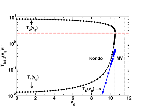
Local electrical gating can shift in energy the localized orbital and thus break particle-hole symmetry. This drives strong thermoelectric effects in the tunneling current, associated to spectral asymmetries in the tunneling spectrum. However, in the standard picture of the Kondo resonance, it is schematically assumed that the Kondo peak is pinned exactly at the Fermi level, independently on the depth of the localized state. While this picture is approximately true and amply sufficient to understand roughly the temperature dependence of the linear conductance in the Kondo regime, it is in fact totally inadequate for describing the thermopower of quantum dots 29. For gate voltages close to the middle of odd charge Coulomb diamonds, the Kondo resonance peak energy differs very little from (by much less than ), due to nearly complete realization of particle-hole symmetry. In this regime, thermal transport also nearly vanishes due to compensating contributions from electron and hole states. However, this energy shift of the Kondo resonance increases to reach as much as about for gate voltages approaching the mixed valence regime in which the charge on the dot can freely fluctuate, and where one can also anticipate enhanced thermoelectric effects (Fig. 1d) 30.
This asymmetry of the Kondo resonance about the Fermi level, along with its strong temperature dependence, are crucial for understanding the low temperature thermopower of Kondo-correlated quantum dots29, 31. Although well established by theory 32, these properties have not been directly observed by experiments to date. This is mainly because parasitic voltage offsets are unavoidable in low temperature transport experiments, due to the signal amplification chain or thermoelectricity in the wiring, rendering the precise determination of the Fermi level , and thus the relative position of the Kondo peak with respect to , difficult. The situation is different when, in addition to a voltage bias, a temperature bias can be applied across a junction hosting the Kondo resonance, leading to thermoelectric effects. Experimentally, the Seebeck coefficient (or thermopower) is defined as in the linear regime, with the thermo-voltage established at zero DC current flowing. While the low-temperature linear conductance probes the amplitude of the junction spectral function at , the low temperature thermopower is related to the spectral function derivative, . More generally, a non-zero Seebeck coefficient in the Kondo state implies that the Kondo resonance must be asymmetric about the Fermi level within a temperature window . Yet, thermoelectric measurements in the presence of Kondo correlations have remained rare to date33 and have either focused on the mixed valence regime15 or on measurements of the thermocurrent rather than Seebeck coefficient34.
Here, we report on a direct measurement of the Seebeck coefficient from the Coulomb blockade to the Kondo regimes, using combined transport and thermopower measurements in a single quantum dot junction. From the variations of the thermopower with level depth at different temperatures, we experimentally verify two hallmarks of Kondo correlations in thermal transport. First, we report on a Seebeck signal that is breaking the -periodicity with respect to the quantum dot charge state, which gives strong indication for single-spin induced effects on thermoelectric properties. Second, we find sign changes in the thermopower upon increasing temperature for fixed gate voltages in the Kondo-dominated odd-charge diamonds, while no such sign change is observed in the non-Kondo even-charge Coulomb diamonds (for fixed gate voltage). The former reflects the intricate spectral weight rearrangement of the asymmetric Kondo resonance from low to high energies as the Kondo peak is destroyed upon increasing temperature (see Fig. 1, as well as Fig. S6 in the Supporting Information). These observations are found in good agreement with predictions from NRG calculations on the Anderson model described in Ref. 29 and further developed in this work.
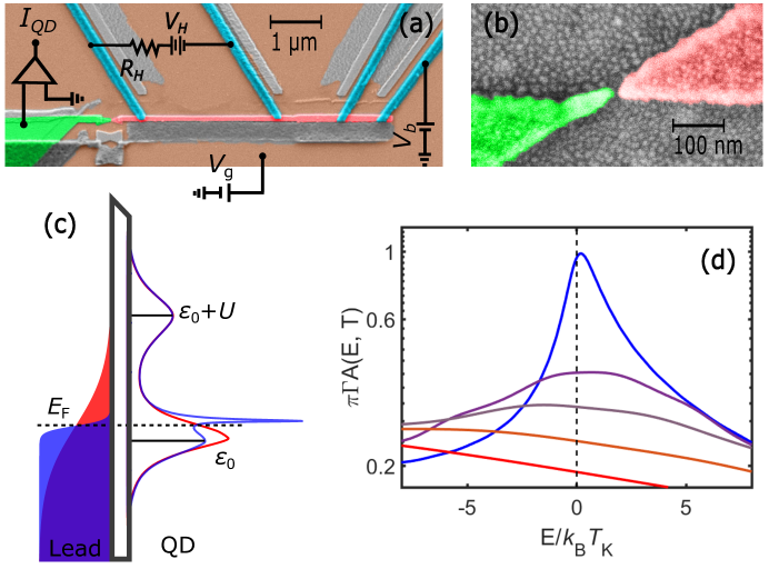
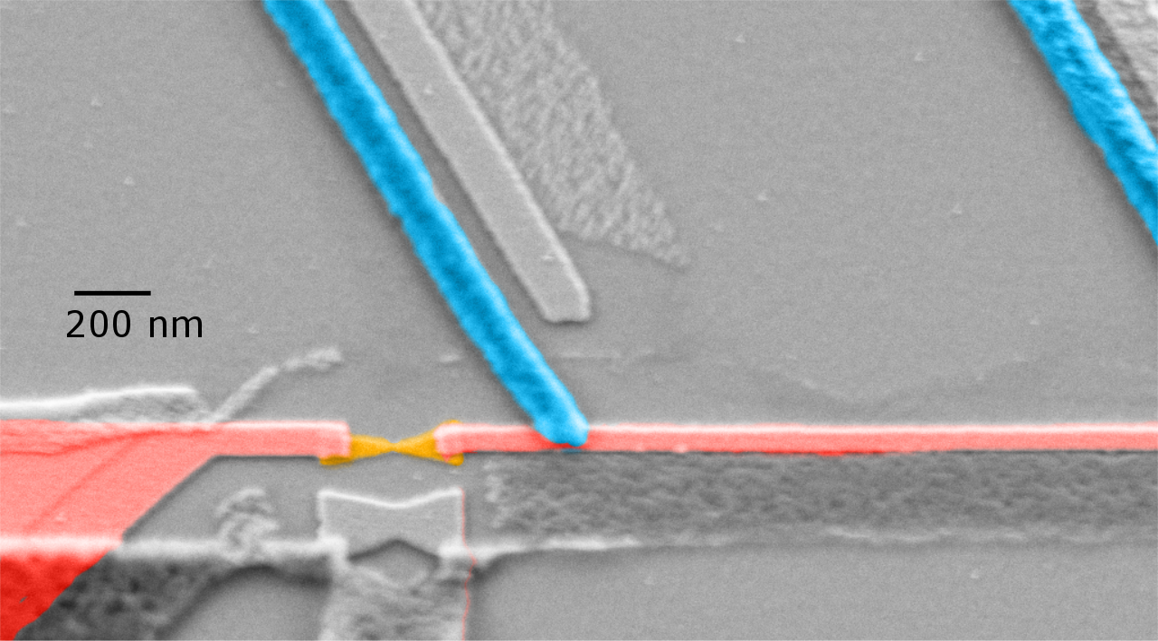
Our junctions are realized using the electromigration technique, which has been successfully applied for studying the Kondo effect in a variety of single quantum dot systems, such as single molecules and metallic nanoparticles25, 35, 36. Using electron-beam lithography and a three-angle shadow evaporation we fabricate devices such as pictured in Fig. 1a, on top of a local back gate. After lift-off, inspection and thus exposure to air, we again evaporate a 1 - 1.5 nm gold layer over the entire sample surface. Due to its extreme thinness, this layer segregates into a discontinuous film of Au nanoparticles37. After cooling to 4.2 K, we form a nm-scale gap in the platinum constriction visible in Fig. 1b by controlled electromigration. Devices displaying reproducible gate-dependent conductance features are then investigated at temperatures down to 60 mK in a thoroughly filtered dilution cryostat. The transport properties are determined by measuring the junction current as a function of the bias voltage and a gate voltage , applied from a local back gate. One lead of the quantum dot junction, defined as the drain in what follows, rapidly widens away from the electromigration constriction, allowing for efficient heat draining on that side. In order to allow the application of a controlled temperature gradient, a normal metallic wire of length 5 m provides the other contact to the quantum dot junction, called the source. The source side of the junction lead displays four high-transparency superconducting aluminum contacts. These allow for electrically connecting while thermally isolating the source at low enough temperatures. Further, we can heat the source electrons by applying a current between two such leads. In principle, the superconducting transport properties between two nearby leads across the source can also be used for local electron thermometry, but due to one missing contact, this was not available in this experiment.
Figure 2a,b shows the differential conductance map of the device, as a function of bias and gate voltage. Four Coulomb diamonds, separated by the degeneracy points of the quantum dot charge states, can be seen and point to a dot charging energy meV (in notation of the Anderson impurity model introduced below). In the device studied here, a second quantum dot appears as a faint conductance feature near V seen in the global transport map of Fig. 2a. It has very different transport characteristics and is discussed in more detail in Sec. III of the Supporting Information. Notably, the thermopower signal associated to the latter appeared only in a very small gate voltage window, well separated from that of the more strongly coupled quantum dot. The gate voltage region above V was subject to electrostatic switches, which did not allow accessing quantitatively the full amplitude of the device response in this region. In two non-adjacent Coulomb diamonds of the main device ( V and 3.5 V V), a transport resonance near zero bias is observed near the degeneracy points. This points to a Kondo resonance based on the degeneracy of the electronic spin doublet in oddly occupied charge states. From the temperature dependence of the resonance amplitude (Figure 2c) we can estimate the value of , which decreases with moving towards , that is, for approaching the center of the odd Coulomb diamond 20.
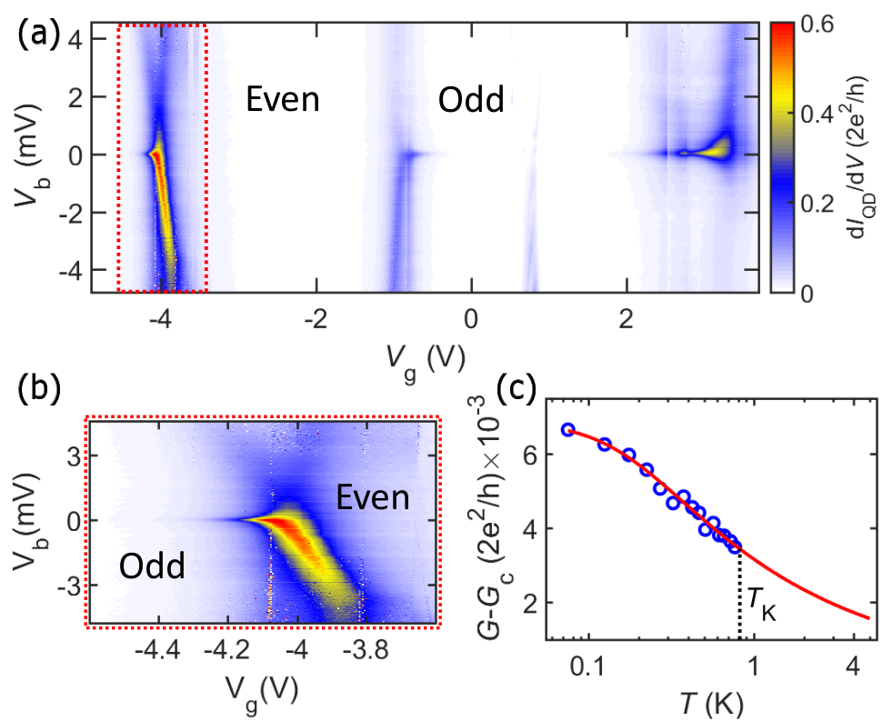
The peak conductance of the Kondo resonance saturates at values in the low temperature limit, from which we can infer that the quantum dot is rather asymmetrically tunnel coupled 38. This asymmetry simplifies the theoretical description, as Kondo correlations can be considered as occurring in equilibrium with the more strongly coupled lead, the other lead acting only as weak probe. In this study, this strongly coupled lead will thus also serve as the only reference for the Fermi level, near which the Kondo resonance develops. The tunnel coupling on the strongly coupled side, meV, can be determined from the widths of the Coulomb diamond edges (see 39 for details pertaining to effects related to the charge parity on the quantum dot, that we have taken into account). As opposed to most experiments based on semiconducting systems, neither the quantum dot nor the tunnel barriers are electrostatically defined here. Thus is essentially independent on the gate voltage here, which simplifies the theoretical comparison.
We now move to the thermoelectric response of the device. We have performed thermoelectric experiments by providing a constant heating power to the source island, leading to three device temperatures, labelled . The lowest temperature is in the range of a 300 mK, while is close to 5 K, and is around 1 K. Details of the estimation of these temperatures is given in Sec. III of the Supporting Information. Measuring the thermopower of a quantum dot junction requires in principle to address the open-circuit voltage of a high-impedance device. This is experimentally challenging, first because the voltmeter itself may shunt the divergent impedance of the device and, second, because the equilibration time to reach the true zero-current state (as required by the definition of the Seebeck coefficient ) at such high impedances can be extremely long. For this reason, several experiments have preferred focusing on the thermocurrent at zero applied bias rather than on the Seebeck coefficient, although only the latter has a direct physical interpretation as a fundamental transport coefficient. In our measurements, we have used the following, to the best of our knowledge, original protocol: at each gate voltage, we sweep the bias voltage and measure the full characteristic (Fig. 3).
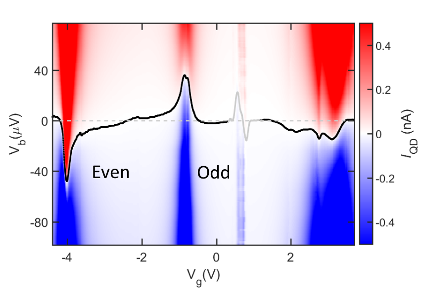
From thereon, we can define as the bias voltage at which the current goes through zero, realizing thus perfect open-circuit conditions. The result is shown as the black line on the same figure. Strikingly, the thermovoltage changes sign at consecutive integer charge states, resulting in a -periodicity of the thermopower response, that directly follows from the presence of Kondo anomalies in odd charge diamonds. In more detail, the -periodicity reflects the fact that the junction spectral function has its maximal weight alternating above and below the Fermi level depending on if the level depth of the doublet spin state is either approaching from below (in which case the dot transits from single to zero occupancy in the active orbital), or from above (in which case the highest occupied electronic orbital starts to become singly occupied and develops the next Kondo ridge).
While this -periodic response of thermopower with the quantum dot charge state is in good agreement with what is expected for the Kondo effect, it is not by itself a proof thereof. Indeed, in a quantum description of the level hybridization, the inclusion of the electron spin degree of freedom leads to a doubling of the spectral function width when the charge states changes parity 39, breaking thus the periodicity naively expected from a sequential or cotunneling description neglecting the spin 40, 41.
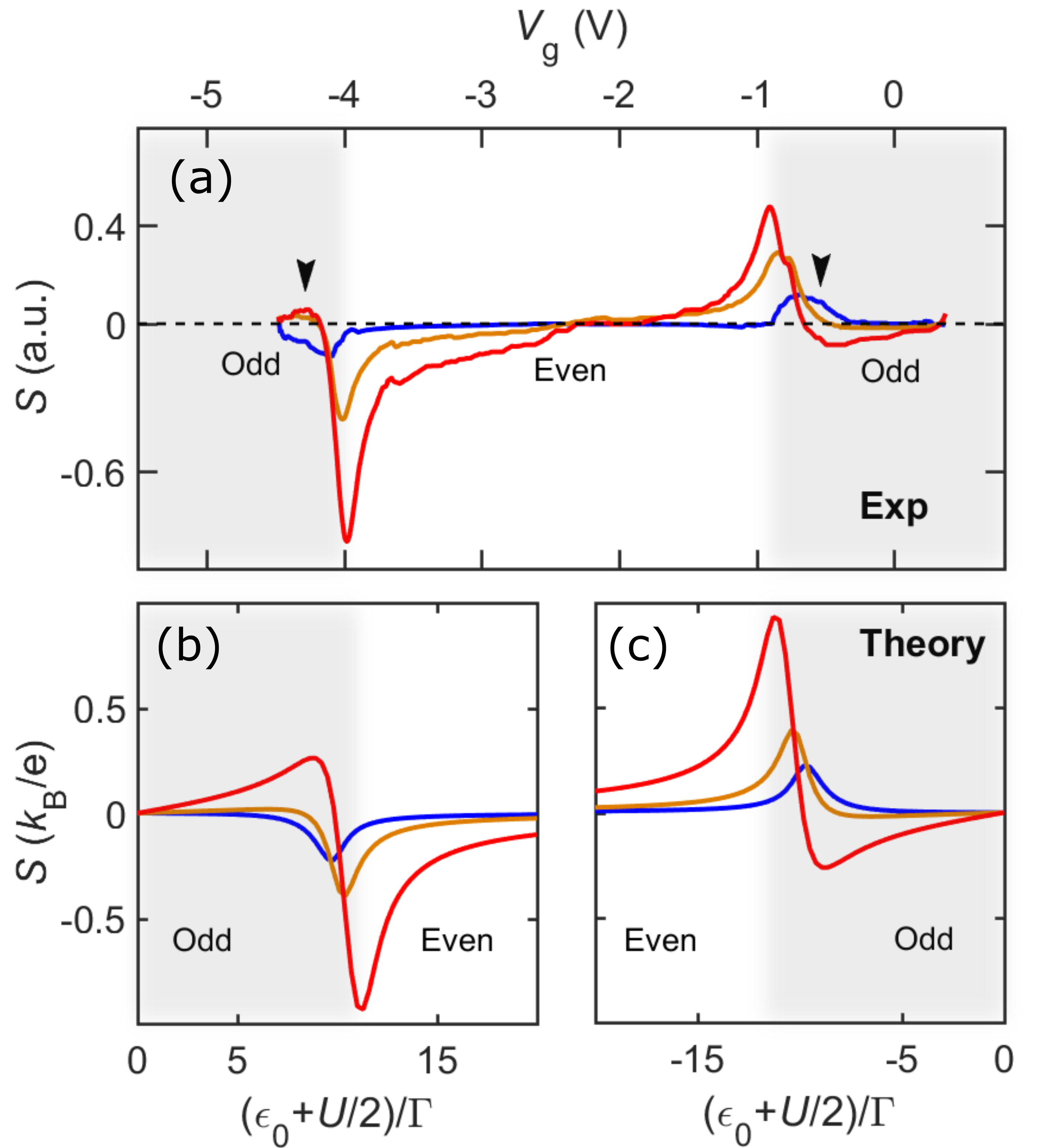
A much more characteristic signature of the singlet nature of the Kondo state resides in multiple sign changes of the thermopower as a function of gate voltage, occuring both in the center of Coulomb-blockaded even and odd charge states, but also at the onset of the Kondo regime within the odd charge diamond. This Kondo-related sign change takes place as temperature is increased from below to above a characteristic temperature , which is a weak function of gate voltage in the Kondo regime (see Fig. S5 of the Supporting Information and Ref. 29). The other Coulomb-related sign changes are temperature independent, and occur when the bare quantum dot energy level is such that (for a single orbital model). In Fig. 4a we show the gate traces of the Seebeck coefficient of the same device at different temperatures. At the lowest temperature (such that ), the thermopower inside the Kondo-correlated Coulomb diamonds (for V and V) has a markedly different behavior with respect to the higher temperature data, confirming this sign change.
Our data can be compared with NRG predictions29 of the Seebeck coefficient of a quantum dot with the parameter value taken from the experiment. The simulations are performed within a two-leads single orbital Anderson impurity model with Hamiltonian:
| (1) |
The first term describes the quantum dot level energy (measured relative to the Fermi level , which is set to zero in our calculations). The dot level is controlled in the experiment with the gate voltage . The second term with charging energy is the local Coulomb repulsion on the dot. The third term describes the Fermi sea in the reservoirs, where labels the two contacts, and is the kinetic energy of the lead electrons. The last term describes the tunneling of electrons from the leads onto and off the dot with tunneling amplitudes . By using even and odd combinations of lead electron states, the odd channel decouples, resulting in a single-channel Anderson model with an effective tunnel matrix element given by . The hybridization is then characterized by the lead-dot tunneling rate , with the lead electron density of states at the Fermi level.
The conductance and thermopower of the Anderson model (1) can be written in terms of the zeroth, and first, , moments of the NRG impurity spectral function within the Fermi temperature window:
| (2) | |||||
| (3) | |||||
| (4) |
where is the zero temperature conductance at midvalley and is the Fermi distribution of the leads at temperature . The above expression for implies that a sign change in the thermopower occurs due to a crossover between the negative (electron-like) and positive (hole-like) energy contributions of the first moment of the spectral function in the Fermi temperature window . At particle-hole symmetric points, such as for perfect integer fillings, e.g., exactly in the middle of even or odd Coulomb diamonds, the spectral function is symmetric about , so that vanishes identically.
The calculated thermopower is plotted in Figs. 4b and 4c as a function of the dimensionless gate voltage , so that the center of the odd charge Coulomb diamond at is clearly identified by a trivially vanishing Seebeck coefficient at that point for any temperature (due to exact particle-hole symmetry). Strikingly, the thermopower anomaly seen near the mixed valence regime presents two distinct regimes: at low temperature, a small thermoelectric signal occurs with a fixed sign, while at high temperature a larger signal displays a clear sign change as a function of gate voltage, defining a crossover temperature . These predictions compare favorably with the experimental data in Fig. 4a, where the gate-dependent signal shows the same sign inversion at temperatures , depending slightly on the gate voltage (see Fig. S5 of Supporting Information). Ultimately, this sign change of the Seebeck coefficient upon increasing temperature from to reflects the spectral weight rearrangement of the asymmetrically located Kondo resonance about (see Fig. 1d, and Sec. IV of the Supporting Information for details).
In conclusion, this work provides a direct measurement of the Seebeck coefficient for a Kondo-correlated single quantum dot tunnel coupled to purely thermal-biased reservoirs. In particular, our measurements bring compelling experimental evidence for a frequently overseen property of the Kondo effect occurring between a spin-degenerate local level and an electron reservoir. By measuring the temperature and gate dependence of the Seebeck coefficient in a single quantum dot junction, we find that it exhibits characteristic sign changes in the Kondo regime upon increasing temperature, which reflect the strong temperature dependence of the Kondo peak that is not exactly pinned at the reservoir Fermi level, as predicted by theory. This work finally demonstrates that electromigrated single quantum dot junctions can now be integrated into more complex circuits, including local electronic heaters and thermometers. This development paves the way for precisely accessing the thermoelectric figure of merit of individual molecules, which requires measuring simultaneously the charge and heat conductance as well as the thermopower, for a large spectrum of molecular devices.
This work has received funding from the European Union’s Horizon 2020 research and innovation programme under the Marie Skłodowska-Curie grant agreement No 766025. B.D. acknowledges support from the Nanosciences Foundation, under the auspices of the Université Grenoble Alpes Foundation. The samples were realized at the Nanofab platform at Institut Néel, with extensive help from T. Crozes. We are deeply indebted to F. Taddei for theoretical guidance about the cotunneling analysis of the thermovoltage. Supercomputer support by the John von Neumann Institute for Computing (Jülich) is gratefully acknowledged. We further acknowledge inspiring discussions with N. Roch and J. Pekola.
References
- Bergfield and Ratner 2013 Bergfield, J. P.; Ratner, M. A. Forty years of molecular electronics: Non-equilibrium heat and charge transport at the nanoscale. Phys. Status Solidi B 2013, 250, 2249–2266
- Thoss and Evers 2018 Thoss, M.; Evers, F. Perspective: Theory of quantum transport in molecular junctions. The Journal of Chemical Physics 2018, 148, 030901
- Pustilnik and Glazman 2004 Pustilnik, M.; Glazman, L. Kondo effect in quantum dots. J. Phys. Cond. Matter 2004, 16, R513
- Grobis et al. 2007 Grobis, M.; Rau, I. M.; Potok, R. M.; Goldhaber-Gordon, D. Kondo effect in mesoscopic quantum dots, in Handbook of Magnetism and Magnetic Materials; Wiley, 2007; Vol. 2
- Bulla et al. 2008 Bulla, R.; Costi, T. A.; Pruschke, T. Numerical renormalization group method for quantum impurity systems. Rev. Mod. Phys. 2008, 80, 395–450
- Schwab et al. 2000 Schwab, K.; Henriksen, E. A.; Worlock, J. M.; Roukes, M. L. Measurement of the quantum of thermal conductance. Nature 2000, 404, 974–977
- Meschke et al. 2006 Meschke, M.; Guichard, W.; Pekola, J. P. Single-mode heat conduction by photons. Nature 2006, 444, 187–190
- Jézouin et al. 2013 Jézouin, S.; Parmentier, F. D.; Anthore, A.; Gennser, U.; Cavanna, A.; Jin, Y.; Pierre, F. Quantum Limit of Heat Flow Across a Single Electronic Channel. Science 2013, 342, 601–604
- Dutta et al. 2017 Dutta, B.; Peltonen, J.; Antonenko, D.; Meschke, M.; Skvortsov, M.; Kubala, B.; König, J.; Winkelmann, C. B.; Courtois, H.; Pekola, J. Thermal conductance of a single-electron transistor. Phys. Rev. Lett. 2017, 119, 077701
- Reddy et al. 2007 Reddy, P.; Yang, S.; Segalman, R.; Majumdar, A. Thermoelectricity in molecular junctions. Science 2007, 315, 1568
- Widawsky et al. 2011 Widawsky, J. R.; Darancet, P.; Neaton, J. B.; Venkataraman, L. Simultaneous determination of conductance and thermopower of single molecule junctions. Nano Lett. 2011, 12, 354–358
- Evangeli et al. 2015 Evangeli, C.; Matt, M.; Rincon-Garcia, L.; Pauly, F.; Nielaba, P.; Rubio-Bollinger, G.; Cuevas, J. C.; Agrait, N. Quantum Thermopower of Metallic Atomic-Size Contacts at Room Temperature. Nano Lett. 2015, 15, 1006–1011
- Cui et al. 2018 Cui, L.; Miao, R.; Wang, K.; Thompson, D.; Zotti, L. A.; Cuevas, J. C.; Meyhofer, E.; Reddy, P. Peltier cooling in molecular junctions. Nature Nanotechnology 2018, 13, 122
- Staring et al. 1993 Staring, A.; Molenkamp, L.; Alphenaar, B.; Van Houten, H.; Buyk, O.; Mabesoone, M.; Beenakker, C.; Foxon, C. Coulomb-blockade oscillations in the thermopower of a quantum dot. EPL (Europhys. Lett.) 1993, 22, 57
- Scheibner et al. 2005 Scheibner, R.; Buhmann, H.; Reuter, D.; Kiselev, M.; Molenkamp, L. Thermopower of a Kondo spin-correlated quantum dot. Phys. Rev. Lett. 2005, 95, 176602
- Svensson et al. 2013 Svensson, S. F.; Hoffmann, E. A.; Nakpathomkun, N.; Wu, P. M.; Xu, H.; Nilsson, H. A.; Sánchez, D.; Kashcheyevs, V.; Linke, H. Nonlinear thermovoltage and thermocurrent in quantum dots. New Journal of Physics 2013, 15, 105011
- Josefsson et al. 2018 Josefsson, M.; Svilans, A.; Burke, A. M.; Hoffmann, E. A.; Fahlvik, S.; Thelander, C.; Leijnse, M.; Linke, H. A quantum-dot heat engine operating close to the thermodynamic efficiency limits. Nature Nanotechnology 2018, 13, 920
- Kim et al. 2014 Kim, Y.; Jeong, W.; Kim, K.; Lee, W.; Reddy, P. Electrostatic control of thermoelectricity in molecular junctions. Nature Nanotechnology 2014, 9, 881
- Glazman and Raikh 1988 Glazman, L.; Raikh, M. Resonant Kondo transparency of a barrier with quasilocal impurity states. JETP Lett. 1988, 47, 452–455
- Goldhaber-Gordon et al. 1998 Goldhaber-Gordon, D.; Shtrikman, H.; Mahalu, D.; Abusch-Magder, D.; Meirav, U.; Kastner, M. Kondo effect in a single-electron transistor. Nature 1998, 391, 156
- Cronenwett et al. 1998 Cronenwett, S. M.; Oosterkamp, T. H.; Kouwenhoven, L. P. A tunable Kondo effect in quantum dots. Science 1998, 281, 540–544
- Pustilnik and Glazman 2001 Pustilnik, M.; Glazman, L. Kondo effect in real quantum dots. Phys. Rev. Lett. 2001, 87, 216601
- Sasaki et al. 2000 Sasaki, S.; De Franceschi, S.; Elzerman, J.; Van der Wiel, W.; Eto, M.; Tarucha, S.; Kouwenhoven, L. Kondo effect in an integer-spin quantum dot. Nature 2000, 405, 764
- Yu and Natelson 2004 Yu, L. H.; Natelson, D. The Kondo effect in C60 single-molecule transistors. Nano Lett. 2004, 4, 79–83
- Roch et al. 2008 Roch, N.; Florens, S.; Bouchiat, V.; Wernsdorfer, W.; Balestro, F. Quantum phase transition in a single-molecule quantum dot. Nature 2008, 453, 633
- Iftikhar et al. 2018 Iftikhar, Z.; Anthore, A.; Mitchell, A.; Parmentier, F.; Gennser, U.; Ouerghi, A.; Cavanna, A.; Mora, C.; Simon, P.; Pierre, F. Tunable quantum criticality and super-ballistic transport in a “charge” Kondo circuit. Science 2018, eaan5592
- Frisenda et al. 2015 Frisenda, R.; Gaudenzi, R.; Franco, C.; Mas-Torrent, M.; Rovira, C.; Veciana, J.; Alcon, I.; Bromley, S. T.; Burzurí, E.; Van der Zant, H. S. Kondo effect in a neutral and stable all organic radical single molecule break junction. Nano Lett. 2015, 15, 3109–3114
- Kondo 1964 Kondo, J. Resistance minimum in dilute magnetic alloys. Progress of theoretical physics 1964, 32, 37–49
- Costi and Zlatić 2010 Costi, T.; Zlatić, V. Thermoelectric transport through strongly correlated quantum dots. Phys. Rev. B 2010, 81, 235127
- Dong and Lei 2002 Dong, B.; Lei, X. Effect of the Kondo correlation on the thermopower in a quantum dot. Journal of Physics: Condensed Matter 2002, 14, 11747
- Costi et al. 1994 Costi, T.; Hewson, A.; Zlatic, V. Transport coefficients of the Anderson model via the numerical renormalization group. Journal of Physics: Condensed Matter 1994, 6, 2519
- Hewson 1997 Hewson, A. C. The Kondo problem to heavy fermions; Cambridge university press, 1997; Vol. 2
- Thierschmann 2014 Thierschmann, H. Ph.D. thesis; University of Würzburg, 2014
- Svilans et al. 2018 Svilans, A.; Josefsson, M.; Burke, A. M.; Fahlvik, S.; Thelander, C.; Linke, H.; Leijnse, M. Thermoelectric characterization of the Kondo resonance in nanowire quantum dots. arXiv preprint arXiv:1807.07807 2018,
- Park et al. 2002 Park, J.; Pasupathy, A. N.; Goldsmith, J. I.; Chang, C.; Yaish, Y.; Petta, J. R.; Rinkoski, M.; Sethna, J. P.; Abruña, H. D.; McEuen, P. L. Coulomb blockade and the Kondo effect in single-atom transistors. Nature 2002, 417, 722
- Liang et al. 2002 Liang, W.; Shores, M. P.; Bockrath, M.; Long, J. R.; Park, H. Kondo resonance in a single-molecule transistor. Nature 2002, 417, 725
- Bolotin et al. 2004 Bolotin, K.; Kuemmeth, F.; Pasupathy, A.; Ralph, D. Metal-nanoparticle single-electron transistors fabricated using electromigration. Applied Phys. Lett. 2004, 84, 3154–3156
- Simmel et al. 1999 Simmel, F.; Blick, R.; Kotthaus, J.; Wegscheider, W.; Bichler, M. Anomalous Kondo effect in a quantum dot at nonzero bias. Phys. Rev. Lett. 1999, 83, 804
- Aligia et al. 2015 Aligia, A.; Roura-Bas, P.; Florens, S. Impact of capacitance and tunneling asymmetries on Coulomb blockade edges and Kondo peaks in nonequilibrium transport through molecular quantum dots. Phys. Rev. B 2015, 92, 035404
- Beenakker and Staring 1992 Beenakker, C.; Staring, A. Theory of the thermopower of a quantum dot. Phys. Rev. B 1992, 46, 9667
- Turek and Matveev 2002 Turek, M.; Matveev, K. Cotunneling thermopower of single electron transistors. Phys. Rev. B 2002, 65, 115332
Supporting information for “Direct measurement of the Seebeck coefficient in a Kondo-correlated single quantum dot transistor”
This supporting information discusses the sample fabrication process, the electrical characterization of the Kondo-correlated quantum dot, the determination of average temperatures of the device under heating conditions, and gives an outline of the theory of the thermoelectric properties of Kondo correlated quantum dots, relevant to the present paper. Numerical Renormalization Group (NRG) calculations provide also new insights and detailed analysis on the thermopower of these systems.
1 I - Sample fabrication
We fabricate the sample on a 2 inch Si 100 wafer with a 500 nm thermal oxide. The first step of the fabrication process is the gate layer. We use a metallic plane covered with an oxide layer as the gate of the quantum dot device. The reason for choosing this local back-gate is that, using this gate configuration, we can easily achieve a very small distance ( 10 nm) between the gate and the gold nano-particles and thereby achieve a strong gate coupling. We use laser lithography to pattern the gate structures on top of a cleaned Si wafer coated with a double layer of photo resists LOR3A/S1805. After development of the exposed area, we evaporate 3 nm titanium (Ti), 30 nm of gold (Au) and again 3 nm of Ti. Both Ti layers act as an adhesive for the following layers. After liftoff and cleaning, the wafer with metallic gate structures is coated with an approximately 8 nm of layer using the atomic layer deposition (ALD) technique.
We designed the main parts of the quantum dot device on top of this gate using electron-beam lithography. The source, constriction, drain and the four probes of the device are patterned on top of the processed wafer coated with a double layer of e-beam resists P(MMA-MAA) 9 and PMMA 4 . After development of the exposed area, we load the sample in an e-beam evaporator with rotatable sample stage to evaporate metals. First, we deposit 11 nm of platinum (Pt) at an angle of w.r.t. the source of the evaporator, this forms the bow-tie shaped constriction of the device, indicated by yellow color in Fig. S1. Then we rotate the sample stage and deposit 25 nm of Au at an angle of , which forms the source and drain of the device (red color in Fig. S1), on top of the Pt constriction. At the same angle, a 3 nm of is then deposited to protect the Au layer from intermixing with the following aluminum (Al) layer. After that we rotate the sample to and deposit 80 nm thick Al contacts, which form the four Al probes on top of the Au source with a clean interface (cyan color in Fig. S1), making four junctions. After liftoff with acetone, IPA and cleaning with plasma, the device is ready for the nano-particle deposition.
In order to form the gold nano-particles, we evaporate 1-1.5 nm of Au on top of the as-made sample. Due to extreme thinness and to surface tension forces, the evaporated Au forms a self-assembled layer nano-particles on top of the sample 1. An SEM image of such evaporated nano-particles is shown in Fig. 1(b) of the main paper. The average size of the gold nano-particles lies in the range of 5-10 nm, which serves as the quantum dot in our device. The advantage of this technique of nano-particle deposition is that, due to high density of the nano-particles the yield of successful single-quantum dot device is rather high (about 70 ).
To complete the fabrication process and place a quantum dot in between the and lead, we electromigrate the constriction, by passing a current through it in a controlled manner 2, 3, 4. As a result, a nano-gap is created between the and leads, bridged by one or sometimes several of the previously deposited gold nano-particles. In order to achieve a strong tunnel coupling between the leads and quantum dot, we perform the electromigration inside the cryostat at 4 K and under cryogenic vacuum.
2 II - Characterization of the quantum dot junction
2.1 Quantum dot parameters
The linear-conductance map of the quantum dot junction is shown in Fig. 2(a) of the paper. The parameters of the quantum dot can be extracted from this conductance map. The positive and negative slopes of the Coulomb diamond edges for the Kondo-coupled quantum dot gives the estimation of the gate coupling factor, also known as lever-arm, 0.02 and the capacitive asymmetry between the source and drain . The gate voltage difference between the two consecutive charge degeneracy points gives the estimate of the charging energy () of the Kondo-coupled quantum dot as 58 meV. The relative contrast of the two Coulomb edges indicates a strong asymmetry in the tunnel coupling of the quantum dot to the leads. The total tunnel rate can be extracted from the width of the Coulomb edges as meV K, taking into account charge parity effects on the renormalization of the linewidth 5.
The weakly-coupled dot, which is coupled in the gate voltage range 0.6 V 1 V, is characterized in the same way. The slopes of the Coulomb diamond edges give the estimate of the lever-arm 0.02. The charging energy U/2 of the weakly coupled quantum dot cannot be measured exactly since we have not observed any other diamond corresponding to this quantum dot . Therefore only a lower limit can be given as U/2 200 meV.
2.2 Study of Kondo Effect
The Kondo spin-singlet formed by the unpaired electron in the quantum dot and the conduction electrons with opposite spin in the lead forms below the characteristic Kondo temperature 6. We characterize the Kondo effect in the quantum dot junction in two different ways, firstly, by measuring the Kondo-resonance peak as a function of temperature and secondly, by measuring the splitting of the Kondo-resonance with the application of a magnetic field 7.
The Kondo-resonance is very sensitive to the temperature, and the DC value of the conductance at zero-bias reduces with temperature. One can extract by fitting the temperature dependence of the conductance at the Kondo-resonance with the empirical formula based on NRG simulations 8, 9:
| (S1) |
where is the saturation value of the conductance at the lowest bath temperature. In the case of a symmetric coupling of the leads to the quantum dot , , the quantum of conductance. But for an asymmetric tunnel coupling only a fraction of the quantum-conductance is achieved in the zero temperature limit, since the Kondo-resonance develops only with the strongly coupled lead while the other lead acts as a probe 10. is the background conductance due to the direct tunnelling or conduction through a highly resistive shunt across the quantum dot junction. Here, one can set phenomelogically for the spin-1/2 Kondo-effect.
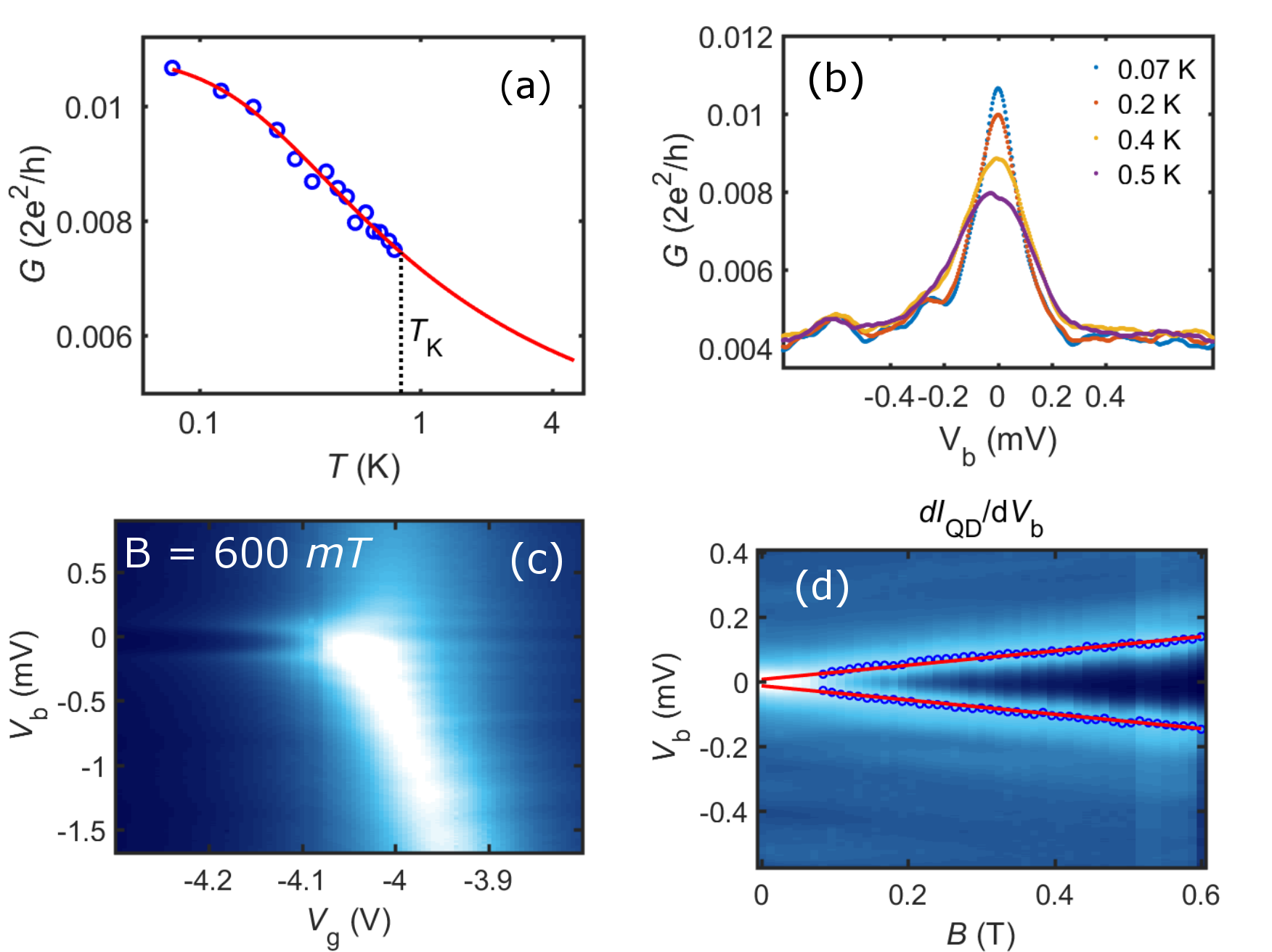
The Kondo-temperature is defined as the temperature at which the Kondo-conductance peak value is reduced to 50 of the conductance peak at the lowest temperature 9. Therefore, using the above formula, . Fig. S2 (a) shows the evolution of the Kondo-conductance peak with temperature at a fixed gate voltage V. The red solid-curve shows the fitting of the data with the above formula, using and as the fitting parameters. From the fit we extract the Kondo temperature of the quantum dot junction at the same gate position as K and a tunnel coupling asymmetry .
Another, but less precise way to determine the Kondo temperature is by perturbing the Kondo state with the application of a magnetic field. A large splitting of the Kondo peak at a fixed magnetic field of mT is shown in Fig. S2 (c). The splitting develops beyond at a critical magnetic field so that , where is the Bohr magneton and is the Landé g-factor (note that this scale differ by a numerical prefactor from the Kondo scale determined above using the temperature dependence of the zero-bias conductance). We measured the conductance of the quantum dot junction as a function of bias and magnetic field. The conductance of the quantum dot junction at a constant gate voltage, with varying magnetic field and bias is plotted in Fig. S2 (d). The splitting of the Kondo-resonance is resolved at a magnetic field 60 . In addition, since splitting of the level is proportional to the applied bias at large bias, it can be fitted with a linear equation, . The fitted red lines in Fig. S2 (d) give an estimate of the Landé-g factor , that is somewhat larger than what is usually found in gold nanoparticles 1. Using the measured critical field that is necessary to split the Kondo resonance, we deduce from this procedure an approximate estimate of the Kondo temperature mK, that is of the same magnitude but somewhat smaller than the Kondo scale extracted from the temperature dependence.
3 III - Thermoelectric measurement
3.1 Experimental temperatures under heating conditions
The experimental device temperature and the thermal gradients under which the three thermopower traces shown in Fig. 4 of the main paper have been obtained cannot be controlled independently in the experiment, as they depend on the thermalization process of the device under the applied heating. The thermal experimental conditions of the three measurements are summarized in TABLE S1.
| Exp | (K) | (nW) | (K) |
|---|---|---|---|
| 0.075 | 0.001 | 0.52 | |
| 0.075 | 2.7 | 2.5 | |
| 4.2 | 2.7 | 5 |
There is an evident hierarchy in the set of operation temperatures. We give here upper bounds on each of these, simply by making a heat-balance between the input constant Joule heating to the source island and the heat leak associated to electron-phonon coupling ,
where relates the steady state heat flow to the interaction volume of the source island, the electron-phonon interaction constant11 in gold W.m-3.K-5 and the two respective temperatures. Such an analysis has been successfully applied in several previous works (see 12 for example). Because heat can leak out of the source side of the device also by other channels, mainly by electronic conduction through the leads, the true device temperature must be substantially below that such estimate, in particular at temperatures higher than several hundred mK, at which the superconductivity in the leads is weakened.
At a cryostat temperature of 4.2 K, the electron-phonon coupling (and thermal conductances of the leads and of the substrate) are large. Thus the thermal imbalance created across the junction using a heating power of 2.7 nW is barely sufficient to heat the source electrode to 5 K. At a cryostat temperature of 75 mK, a heating power of 1 pW will lead to mK if one neglects all other heat leak channels. At the same cryostat temperature, a heating power of 2.7 nW cannot heat the device above 2.5 K following the above arguments, but the true device temperature is presumably closer to 1 K. Because , the estimations of the are evidently an upper bound to the device average temperature in each case.
In conclusion, is of the order of 300 mK, is slightly above 4 K and has an intermediate value, on the order of 1 K. These estimates have been taken for the temperatures used in the Numerical Renormalization Group (NRG) calculations, with an hybridization 30 K. The obtained theoretical predictions for the thermopower, shown in Fig. 4b)c) of the main manuscript, are in good agreement with the experimental measurement of Fig. 4a).
3.2 Thermovoltage signal: Kondo dot vs weak dot
The measurement of the thermovoltage of the quantum dot junction shows clearly distinct features for the Kondo-coupled dot and the weakly coupled dot respectively. The thermovoltage is determined in the same manner as described in the main paper: we increase the bias across the quantum dot junction and measure the current and therefrom define the thermovoltage as the voltage bias where the measured current becomes zero. The current map of the quantum dot junction with the black line-trace for the thermovoltage is shown in Fig. S3.
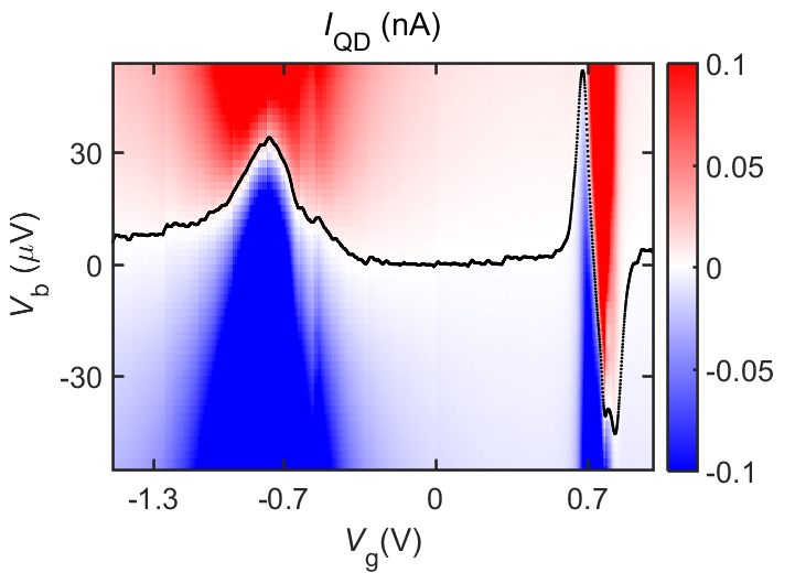
As it can be seen in the figure, the thermovoltage signal for the Kondo-coupled dot in the gate voltage range has a positive sign, while for the dot that is coupled in the gate voltage range , the thermovoltage signal has both positive and negative sign and passing through zero at the degeneracy point at V, which is the expected thermovoltage-signature of a weakly coupled dot 13, 14.
4 IV - Numerical Renormalization Group approach to thermoelectricity
In the following, we describe the parameter regimes of the model used to describe the thermopower of Kondo correlated quantum dots, outline the transport calculations via the numerical renormalization group, summarize the temperature and gate voltage dependence of the thermopower 15 and provide a more detailed analysis of the temperature induced sign changes of the thermopower in the Kondo regime. In particular, we explain the origin of the sign change at in terms of a temperature dependent spectral weight shift of the asymmetrically located Kondo resonance. Finally, estimates for the gate voltage dependence of for the parameters of the experiment are given.
4.1 Model and parameter regimes
In order to describe the thermoelectric transport through a strongly correlated quantum dot we use a two-lead single-level Anderson impurity model. The Hamiltonian is given by . The first term, , describes the dot Hamiltonian, where is the level energy, measured relative to the Fermi level , is the occupation number for spin electrons in the dot level, and is the local Coulomb repulsion on the dot. The second term describes the Hamiltonian of the leads and is given by , where labels the two leads, and is the kinetic energy of the lead electrons. The last term, , describes the tunneling of electrons from the leads onto and off the dot with tunneling amplitudes . By using even and odd combinations of lead electron states, the odd channel decouples, resulting in a single-channel Anderson model with an effective tunnel matrix element given by . The model is then characterized by the lead-dot tunneling rate , with the lead electron density of states at the Fermi level, the level position , and the local Coulomb repulsion . In the real system, the level position is controlled by a gate voltage via , with an arbitrary offset voltage. Equivalently, varying the gate voltage controls the Fermi level and thus . Without loss of generality, we shall set as our zero energy reference throughout.
In describing the theoretical results, it is convenient to define a dimensionless gate voltage which vanishes at the particle-hole symmetric point of the Anderson model, , where the thermopower also (trivially) vanishes. Three different physical regimes are relevant for characterizing and understanding the linear thermoelectric transport properties of the model in the strongly correlated case : (i) the charge fluctuation, or, mixed valence regime, which corresponds to level positions lying within of the Fermi level, i.e., . In this regime, the charge on the dot, , fluctuates between approximately and electrons so the average occupation is approximately (with deviations from this value depending on the precise value of in the above range). Another mixed valence regime occurs when . In this case, the charge on the dot fluctuates approximately between and electrons, and the average occupation of the dot is approximately (with the precise value depending on the location of in the above range). For or , the dot occupancy tends to zero, or two electrons, respectively, i.e., to an even number of electrons on the dot. In this empty (or full) orbital regime, many-body interactions become irrelevant, so that a description in terms of an effective noninteracting model becomes possible. Finally, for , i.e., between the above two mixed valence regimes, the dot occupation approaches , charge fluctuations are suppressed by the Coulomb energy , and low energy spin fluctuations give rise to the Kondo effect. For , the Kondo regime occurs for dimensionless gate voltages , the mixed valence regimes occur for and and the empty (full) orbital regimes occur for and .
4.2 Linear thermoelectric transport calculations
The linear thermoelectric transport properties of the above model are calculated in terms of the energy and temperature dependent spectral function of the dot, , where is the excitation energy measured relative to the Fermi level and is the temperature16, 15.
The conductance and thermopower can be written in terms of the zeroth, and first, , moments of the spectral function within the Fermi temperature window as follows:
| (S2) | ||||
| (S3) |
where is the zero temperature conductance at midvalley, and the moments are given by
| (S4) |
where is the Fermi distribution of the leads at temperature
The above expression for makes it clear that a sign change in the thermopower occurs due to a competition between the negative (electron-like) and positive (hole-like) enegy contributions of the moment of the spectral function in the Fermi temperature window . At particle-hole symmetric points, such as for integer fillings, e.g., exactly in the middle of even or odd Coulomb diamonds, the spectral function is symmetric about and vanishes identically.
We use the numerical renormalization group (NRG) method6, 17 to calculate . The NRG uses a discrete approximation to the continuum Anderson model and therefore results in a discrete representation for the spectral function as a set of delta function peaks at the excitation energies of the system, i.e., in the discrete Lehmann representation:
| (S5) |
where and are the eigenvalues and eigenstates of the system and is the partition function. For visualizing , a broadening of the delta functions with Gaussians of widths proportional to the energies of the excitations is necessary. Since the NRG calculates the excitations on a logarithmic scale around , this broadening procedure inevitably leads to an overbroadening of the high-energy spectral features, such as the Hubbard peaks at and , as compared to the low-energy features, such as the Kondo peak at , whose width is correctly resolved by this procedure. This overbroadening of the high energy features can be avoided, to a large extent, by evaluating the spectral function indirectly via the many-body self-energy18. However, the actual calculations of and , from the moments and , do not require a broadened spectral function: the integrations for and can be evaluated analytically using the discrete form of the spectral function to give
| (S6) |
In addition to avoiding any additional errors arising from a broadening procedure, this way of calculating and can be carried out with high precision19, 20, since the above expressions for these moments takes the same form as the calculation of thermodynamic observables within the NRG. Such calculations are known to be essentially exact by comparisons with Bethe-Ansatz calculations21. Hence, the calculations for and , using the moments and obtained with the discrete form of the spectral function, are also essentially exact at all temperatures and for all parameter values. In particular, as compared to a previous study 15 which used the broadened spectral function to calculate and , we are here able to provide some additional insights concerning the detailed behavior of the thermopower (see next subsection).
4.3 Characterization of the results for versus at different
The behaviour of the thermopower as function of temperature exhibits different characteristic behaviour in the three different regimes of the model 15. It suffices to consider just , since the thermoelectric properties for can be obtained via a particle-hole transformation: and . To illustrate the trends, we have used , however, for comparisons with the measurements, calculations were also performed at the experimentally determined value of .
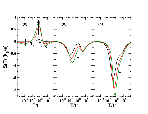
For gate voltages in the mixed valence and empty (full) orbital regimes, the thermopower exhibits no sign changes as function of , see Fig. S4(b)-S4(c). The mixed valence regime does, however, exhibit two peaks in , which merge into a single peak (and a remnant shoulder) in the empty (full) orbital regimes [see Fig. S4(c)].
The most interesting behaviour in the temperature dependence of the thermopower is in the Kondo regime of gate voltages. For fixed , exhibits two sign changes upon increasing from to [see Fig. S4(a)]: one at and a second one at , where is the gate voltage dependent Kondo temperature defined by
| (S7) |
and we have introduced the dimensionless Coulomb energy . The gate voltage dependence of and have been described previously 15. We summarize and expand on this here. and increase (decrease) monotonically from their minimum (maximum) values at midvalley () with increasing and merge to a common value at a critical gate voltage , where is the gate voltage for entry into the mixed valence regime [the mixed valence regime at has ]. The midvalley values and are denoted by and , respectively, and are shown in Table S2 for a range of together with the corresponding midvalley Kondo scales . We note that and exist as limit values and are finite, despite the fact that the thermopower vanishes identically at midvalley: . and are approximate crossing points (isosbectic points) and are a common feature of strongly correlated systems 22. In general, as we verify in more detail below, neither nor are low energy scales, but the former can approach several for smaller or for values of approaching the mixed valence regime when both and the Kondo scale become larger and can be of comparable magnitude.
From Table S2 we see that , i.e., a high energy scale of the Anderson model. A detailed analysis of the data in Table S2 shows that for ,
| (S8) |
At we also find a minimum in the dot occupation . This minimum is absent in the other regimes. For fixed , we find that versus correlates with the dot level position .
Turning now to , an analysis of the data in Table S2 for gives
| (S9) |
with and . Clearly, unlike , is not exponentially decreasing with increasing and cannot, therefore, be considered a low energy scale111This result was anticipated but not demonstrated in Ref. 15. A low energy scale characterizing the Kondo induced peak in the low temperature thermopower is the position of this peak, which has been shown to scale with 15. One sees from Table S2 that typical values of at midvalley are of , even for large values of . While these midvalley values might appear to be irrelevant for experiments, as vanishes identically there, they are nevertheless relevant since they can be taken as lower bounds for at finite gate voltages, where the thermopower is finite. Moreover, the gate voltage dependence of is rather weak in the Kondo regime and only increases rapidly on approaching the mixed valence regime, where approaches a value of , eventually merging with at as shown in Fig. S5 for the case relevant to the experiment. This allows the Kondo induced sign changes in the thermopower at low, but not exponentially low temperature scales, to be accessed in the temperature range . One sees, for example, that for the whole range (i.e., ) in the Kondo regime that ranges in value between and . Thereby, the experiment is able to access the temperature range (i) for where as well as the temperature range (ii) for where can be positive or negative depending on . From Fig. S5, one can read off, for any fixed gate voltage in the Kondo regime, the temperature at which the thermopower changes sign upon increasing temperature through , or, for any fixed temperature , the gate voltage at which versus changes sign (see next section).
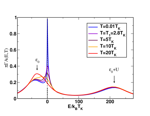
A microscopic understanding of the sign changes in the thermopower at and requires a closer look at the temperature dependence of the spectral function for fixed gate voltage (local level position) in the Kondo regime. This is shown in Fig. S6 for and () at several temperatures. At temperatures we have a fully developed Kondo resonance pinned close to, but slightly above the Fermi level, thereby yielding a negative thermopower due to more hole-like excitations () as compared to electron-like () excitations in the Fermi temperature window . Alternatively, one also sees this from a low temperature Sommerfeld expansion (which, however, is only valid for ):
| (S10) |
Upon increasing temperature, the Kondo resonance is gradually destroyed on a temperature scale of order . In the process, spectral weight from the Kondo resonance is redistributed to higher energies . Initially, most of this weight (for this particular gate voltage ) is shifted to below, rather than above, the Fermi level. Consequently the contribution of electron-like excitations in increase relative to that of the hole-like excitations and this eventually results in a sign change of and hence of at . The above picture, holds generally, and explains the sign change of the thermopower at in terms of the temperature dependent spectral weight shift of the asymmetrically located Kondo resonance. A further increase in temperature expands the Fermi window sufficiently such that the contributions of the incoherent (Hubbard) satellite peaks at and become determining factors in the sign of . The weight of these excitations is approximately and , respectively. The second sign change at corresponds to an increasing population of the hole-like excitations at and a decreasing population of the electron-like excitations at , i.e., at the minimum of vs . Such a minimum, responsible for the sign change of , at , and hence of , is indeed only observed in the Kondo regime15.
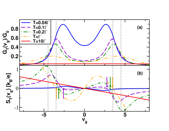
4.4 Characterization of versus at different
The above characteristic temperature dependence of the thermopower in the different regimes of gate voltage can be straightforwardly translated into different characteristic gate voltage dependencies of the thermopower, , in different temperature ranges: (i) , (ii), , and, (iii), . This gate voltage dependence, for temperatures in each of the above ranges, is shown in Fig. S7(b) together with that of the conductance [Fig. S7(a)]. In the first and last temperature ranges (see also Fig. S4), the thermopower exhibits no sign change as a function of (except the trivial one at ), as depicted in Fig. S7(b) for the and curves. In the temperature range (ii) has the opposite sign to that in (i) and (iii) in a range of gate voltages about [delimited by the vertical arrows in Fig. S7(b)]. Outside this range, the thermopower, for fixed , is of the same sign at all temperatures [see the and curves in Fig. S7(b)]. The change in sign of versus at the boundary between these ranges [see the vertical arrows in Fig. S7(b)] and for temperatures in the range (ii) is characteristic of the thermopower of a Kondo correlated quantum dot. It is absent for weakly correlated quantum dots () where there is no sign change in either the - or -dependence of the thermopower (except the trivial one at ) 15.
References
- Bolotin et al. 2004 K. I. Bolotin, F. Kuemmeth, A. N. Pasupathy, and D. C. Ralph, Applied Physics Letters 84, 3154 (2004), https://doi.org/10.1063/1.1695203, URL https://doi.org/10.1063/1.1695203.
- Park et al. 1999 H. Park, A. K. L. Lim, A. P. Alivisatos, J. Park, and P. L. McEuen, Applied Physics Letters 75, 301 (1999), https://doi.org/10.1063/1.124354, URL https://doi.org/10.1063/1.124354.
- Strachan et al. 2005 D. R. Strachan, D. E. Smith, D. E. Johnston, T.-H. Park, M. J. Therien, D. A. Bonnell, and A. T. Johnson, Applied Physics Letters 86, 043109 (2005), https://doi.org/10.1063/1.1857095, URL https://doi.org/10.1063/1.1857095.
- Wu et al. 2007 Z. M. Wu, M. Steinacher, R. Huber, M. Calame, S. J. van der Molen, and C. Schönenberger, Applied Physics Letters 91, 053118 (2007), https://doi.org/10.1063/1.2760150, URL https://doi.org/10.1063/1.2760150.
- Aligia et al. 2015 A. Aligia, P. Roura-Bas, and S. Florens, Phys. Rev. B 92, 035404 (2015).
- Wilson 1975 K. G. Wilson, Rev. Mod. Phys. 47, 773 (1975), URL http://link.aps.org/doi/10.1103/RevModPhys.47.773.
- Grobis et al. 2007 M. Grobis, I. G. Rau, R. M. Potok, and D. Goldhaber-Gordon, Handbook of Magnetism and Advanced Magnetic Materials (2007).
- Costi et al. 1994 T. A. Costi, A. C. Hewson, and V. Zlatic, Journal of Physics: Condensed Matter 6, 2519 (1994), URL http://stacks.iop.org/0953-8984/6/i=13/a=013.
- Goldhaber-Gordon et al. 1998 D. Goldhaber-Gordon, J. Göres, M. A. Kastner, H. Shtrikman, D. Mahalu, and U. Meirav, Phys. Rev. Lett. 81, 5225 (1998), URL https://link.aps.org/doi/10.1103/PhysRevLett.81.5225.
- Simmel et al. 1999 F. Simmel, R. H. Blick, J. P. Kotthaus, W. Wegscheider, and M. Bichler, Phys. Rev. Lett. 83, 804 (1999), URL https://link.aps.org/doi/10.1103/PhysRevLett.83.804.
- Echternach et al. 1992 P. M. Echternach, M. R. Thoman, C. M. Gould, and H. M. Bozler, Phys. Rev. B 46, 10339 (1992), URL https://link.aps.org/doi/10.1103/PhysRevB.46.10339.
- Dutta et al. 2017 B. Dutta, J. T. Peltonen, D. S. Antonenko, M. Meschke, M. A. Skvortsov, B. Kubala, J. König, C. B. Winkelmann, H. Courtois, and J. P. Pekola, Phys. Rev. Lett. 119, 077701 (2017), URL https://link.aps.org/doi/10.1103/PhysRevLett.119.077701.
- Beenakker and Staring 1992 C. W. J. Beenakker and A. A. M. Staring, Phys. Rev. B 46, 9667 (1992), URL https://link.aps.org/doi/10.1103/PhysRevB.46.9667.
- Turek and Matveev 2002 M. Turek and K. A. Matveev, Phys. Rev. B 65, 115332 (2002), URL https://link.aps.org/doi/10.1103/PhysRevB.65.115332.
- Costi and Zlatić 2010 T. A. Costi and V. Zlatić, Phys. Rev. B 81, 235127 (2010), URL http://link.aps.org/doi/10.1103/PhysRevB.81.235127.
- Kim and Hershfield 2002 T.-S. Kim and S. Hershfield, Phys. Rev. Lett. 88, 136601 (2002), URL https://link.aps.org/doi/10.1103/PhysRevLett.88.136601.
- Bulla et al. 2008 R. Bulla, T. A. Costi, and T. Pruschke, Rev. Mod. Phys. 80, 395 (2008), URL http://link.aps.org/doi/10.1103/RevModPhys.80.395.
- Bulla et al. 1998 R. Bulla, A. C. Hewson, and T. Pruschke, Journal of Physics: Condensed Matter 10, 8365 (1998), URL http://stacks.iop.org/0953-8984/10/i=37/a=021.
- Yoshida et al. 2009 M. Yoshida, A. C. Seridonio, and L. N. Oliveira, Phys. Rev. B 80, 235317 (2009), URL http://link.aps.org/doi/10.1103/PhysRevB.80.235317.
- Merker et al. 2013 L. Merker, S. Kirchner, E. Muñoz, and T. A. Costi, Phys. Rev. B 87, 165132 (2013), URL https://link.aps.org/doi/10.1103/PhysRevB.87.165132.
- Merker et al. 2012 L. Merker, A. Weichselbaum, and T. A. Costi, Phys. Rev. B 86, 075153 (2012), URL http://link.aps.org/doi/10.1103/PhysRevB.86.075153.
- Vollhardt 1997 D. Vollhardt, Phys. Rev. Lett. 78, 1307 (1997), URL https://link.aps.org/doi/10.1103/PhysRevLett.78.1307.