An analytic virtual-source-based current-voltage model for ultra-thin black phosphorus field-effect transistors
Abstract
In this paper, we develop an analytic physics-based model to describe current conduction in ultra-thin black phosphorus (BP) field-effect transistors (FETs). The model extends the concept of virtual source charge calculation to capture the effect of both hole and electron charges for ambipolar transport characteristics. The model comprehends the in-plane band-structure anisotropy in BP, as well as the asymmetry in electron and hole current conduction characteristics. The model also includes the effect of Schottky-type source/drain contact resistances, which are voltage-dependent and can significantly limit current conduction in the on-state in BP FETs. Model parameters are extracted using measured data of back-gated BP transistors with gate lengths of 1000 nm and 300 nm with BP thickness of 7.3 nm and 8.1 nm, and for the temperature range of 180 K to 298 K. Compared to previous BP models that are validated only for room-temperature and near-equilibrium bias conditions (low drain-source voltage), we demonstrate excellent agreement between the data and model over a broad range of bias and temperature values. The model is also validated against numerical TCAD data of top-gated BP transistors with a channel length of 300 nm. The model is implemented in Verilog-A and the capability of the model to handle both dc and transient circuit simulations is demonstrated using SPECTRE. The model not only provides a physical insight into technology-device interaction in BP transistors, but can also be used to design and optimize BP-based circuits using a standard hierarchical circuit simulator.
I Introduction
Over the past decade, two dimensional (2D) materials, including graphene,Yarmoghaddam and Rakheja (2017); Rakheja et al. (2013a); Novoselov et al. (2005) transition metal dichalcogenides (TMDC),Wang et al. (2012); Fivaz and Mooser (1967) silicene,Houssa et al. (2011); Vogt et al. (2012) and germanane, Bianco et al. (2013) have emerged as promising candidates for future generations of nanoelectronic devices due to their excellent electrostatic integrity, vertical scalability, and electronic properties that are considerably different from those in their bulk parental materials. Xia et al. (2014a); Das et al. (2014); Yi et al. (2017); Qiao et al. (2014) In graphene, carriers have a limited phase space for scattering, which can allow quasi-ballistic transport at room-temperature. Geim and Novoselov (2007); Hwang and Sarma (2008); Qiao et al. (2014) Several high-frequency devices using graphene have been experimentally demonstrated such as radio-frequency FETs, optical modulators, and photo-detectors. Xia et al. (2014a) However, the use of graphene in digital switching applications is challenging due to its low on-off current ratio, which results from its zero band gap. Han et al. (2014) On the other hand, TMDC-based FETs, with the band gap in the range of () eV, possess high on-off current ratios;Qiao et al. (2014) however, the carrier mobility in TMDCs is much lower than that in graphene.Du et al. (2014)
More recently, black phosphorus (BP) has emerged as one of the most interesting 2D materials for high performance transistor applications.Huang et al. (2017); Haratipour et al. (2016) In its bulk form, BP exhibits a band gap 0.3 eV, while in its monolayer form, the band gap increases to 2 eV. Haratipour et al. (2016); Xia et al. (2014a); Yang et al. (2016) Additionally, the hole mobility in BP is reported to be as high as 1000 cm2/Vs at room-temperature. Bohloul et al. (2016); Haratipour et al. (2016) Because of its puckered crystal structure, there exists a significant difference in the effective mass of carriers along the zigzag and armchair directions, with the armchair direction featuring light mass of carriers. Haratipour et al. (2016); Luo et al. (2015); Xia et al. (2014a); Yang et al. (2016) With its tunable band gap, band-structure anisotropy, and high carrier mobility, BP is an excellent material to implement digital transistors for both high-performance and low-power electronic applications. Xia et al. (2014b); Yang et al. (2016)
To understand, design, and simulate electronic circuits built with BP transistors, a physics-based compact model of current conduction is needed.Rakheja et al. (2014) So far, only a few models that describe current conduction in BP transistors have been reported in the literature Penumatcha et al. (2015); Esqueda et al. (2017). Prior BP FET models are mainly suited for near-equilibrium transport conditions, i.e. when the drain-source bias, , is comparable to the thermal voltage, ( is Boltzmann constant, is the operating temperature, and is the elementary charge). Moreover, these models also do not include the effect of interface traps and non-linear contact resistances, which are important to interpret experimental data. The 2D FET models reported elsewhere either introduce significant empiricism in their approach due to thermally activated and hopping-based transport, Wang et al. (2016, 2017); Cao et al. (2018) or suffer from a limitation of not being able to reproduce the ambipolar characteristics. For example, the current-voltage (I-V) model for short-channel 2D transistors presented in Ref. 29 focuses mainly on intrinsic current conduction, while extrinsic effects due to contacts and traps are not included. The drift-diffusive I-V model presented in Ref. 30 is based on the calculation of the surface potential throughout the channel. However, the desired error-tolerance in the calculation of the surface potential must be in the range of sub-nV, which makes this model susceptible to convergence issues. Additionally, the broad-bias validity of the model in Ref. Marin et al., 2018 requires numerical integration, which increases the computational complexity of the proposed model. As such, the model fit to experimental data has been demonstrated only for a limited bias range (gate-source bias greater than -1.5 V for transfer characteristics and drain-source bias of -1.2 V for output characteristics). Models based on the Landauer transport theory Landauer (1957); Datta (1997) have also been reported in the literature. Penumatcha et al. (2015); Esqueda et al. (2017) In Ref. 24, a Schottky-barrier (SB) model to describe current conduction in off-state is developed. This model is extended in Ref. 25 to cover the on-state regime by including the channel transmission. However, this model is not suited for broad-bias circuit simulations as its validity is restricted to 10 mV at 300 K. We also note that none of the existing compact models for BP transistors has been implemented in Verilog-A to enable device-circuit co-design and optimization.
In this paper, we present an analytic I-V model of BP transistors to capture the ambipolar nature of current conduction over a broad range of bias voltages and temperatures. This model is based on the calculation of channel charges at the virtual source and is an extension of the previously published ambipolar virtual-source model applicable for graphene FETs. Rakheja et al. (2014) This paper extends the model in Ref. 23 in the following key ways. First, the threshold voltage, , for electron and hole conduction is redefined due to the FET structure under study. Second, to handle the nonlinear behavior of Schottky source/drain contacts, we develop a new contact resistance model. Third, the model is extended to capture the low-temperature behavior of BP FETs. The model is validated by applying it to study BP FETs with gate lengths of 1000 nm and 300 nm and with BP thickness of 7.3 nm and 8.1 nm. This model has been implemented in Verilog-A and is used to simulate the circuit behavior of BP-based inverters and ring oscillators.
II Model Description
In transistors with ambipolar current conduction, the net drain-source current, , for a given device width, , is given as Rakheja et al. (2014)
| (1a) | |||
| (1b) | |||
| (1c) |
Note all quantities calculated at the top-of-the-barrier or the virtual source (VS) are denoted with the subscript x0. In the above equation, and are the electron and hole charges, respectively, at the VS point in the channel (see Section II.1 for details.) The velocities, and , are the electron and hole saturation velocities, respectively. The functions, and empirically capture the transition between linear and saturation regimes for the electron and hole branches, respectively. Per this model, it is assumed that there exist two VS points at opposite ends in the channel for electrons and holes. Unlike graphene FETs in which electron and holes typically have similar mobilities and velocities, BP FETs feature different physical properties for electrons and holes. As a result of this difference, () and () are treated separately in this paper. Moreover, in current state-of-the-art technology, the carrier mean free paths in BP FETs are on the order of few 10’s of nanometers. Given that the devices under study have gate lengths on the order of several 100’s of nanometers, we expect transport to be collision dominated Lundstrom and Antoniadis (2014). As such, the velocities in Eq. (1c) are treated as saturation velocities, rather than as injection velocities in the quasi-ballistic transport. This modified interpretation of is similar to that reported in Ref. 34 to handle transport in long-channel gallium nitride transistors using the VS model.
The empirical function ( = for electrons/holes) is given as Rakheja et al. (2014)
| (2) |
In this function, is the intrinsic drain-source voltage drop in the channel, is an empirical parameter, typically in the range of 1.5 to 2.5, and is obtained upon calibration with experimental data, and is the drain-source voltage at which the current conduction changes from linear to saturation regimes. Here, is the channel length and is the mobility of carriers. Details of mobility and its temperature dependence are presented in Section III.
All quantities in Eq. (1c) vary with and , which are the intrinsic gate-source and drain-source voltages, respectively. Intrinsic voltages are given as Rakheja et al. (2014)
| (3a) | |||
| (3b) |
where and denote the external gate-source and drain-source voltage drops, respectively. Contact resistances corresponding to electron and hole branches are denoted as and , respectively. Section II.2 presents the analytic model of contact resistances.
II.1 Channel charge model
The analytic model of electron and hole charges in Eq. (1c), adapted from Ref. Rakheja et al., 2014, are reproduced here for completeness and to drive the discussion that follows.
| (4a) | |||
| (4b) |
where is the gate-channel capacitance in strong inversion, () is the threshold voltage of electron (hole) branch, () is the non-ideality factor of the electron (hole) branch, . The gate-channel capacitance is , where is the oxide permittivity, and is the capacitance equivalent thickness of the oxide. For thick oxides, is approximately equal to the physical thickness of the oxide, . The non-ideality factor incorporates the effect of punch-through () and is given as . Here, is the value of the non-ideality factor when .
The threshold voltage of the electron and hole branches is given as
| (5a) | |||
| (5b) |
Here, corresponds to the ambipolar (minimum-conductivity) point at = 0 V, approximates the effect of interface traps, and and are empirical fitting parameters. The functions and are logistic functions that control the change in the threshold voltage between weak inversion and strong inversion regimes and are given as
| (6a) | |||
| (6b) |
Here, and are introduced as additional fitting parameters to adjust the rate and smoothness of transition of the threshold voltage between its weak inversion and strong inversion limits. Typical values of / and / are in the range of 3-11, depending on the channel length and the type of carriers.
Unlike graphene FETs in which the ambipolar point voltage does not shift with , Rakheja et al. (2013b) in BP FETs, the ambipolar point voltage shows strong dependence on . Haratipour et al. (2016, 2015); Haratipour and Koester (2016) Additionally, the thickness of the BP flakes studied in this work is less than 10 nm, which results in a narrow band gap of BP and a significant carrier injection at the drain end. Therefore, the on-off current ratio decreases by over two orders of magnitude as increases (see Section IV on Results). The dependence of on and the degradation in on-off current ratio with can be captured using the following equation:
| (7) |
where , , and are extracted from experimental calibration. The threshold voltage model uses 11 parameters, out of which seven parameters: , , , and , can be extracted from the transfer curves by measuring the change in the threshold voltage with (see Appendix A for details.) The remainder four parameters: , are tweaked in the range around 3-11 to match the transition between the on and off characteristics of the transistor, as well as to adjust the smoothness of the device transconductance. The validation of the charge model and gate capacitance against numerical data is discussed in Appendix C.
II.2 Contact resistance
The parasitic resistances associated with source and drain contacts in BP FETs are bias-dependent, nonlinear resistances. This is because at the interface between the contact metal and the BP channel, a Schottky barrier is formed, which shows a strong bias dependence. Chang et al. (2014, 2017); Du et al. (2016)
The current, , through a Schottky barrier (SB) for a given voltage drop across it is given as Xu et al. (2016); Chang et al. (2014)
| (8) |
where is the effective junction area of the SB contact, is the Richardson constant, and is the SB height. For purely thermionic emission at the SB contact, the non-ideality factor = 1. For other types of current conduction, such as thermally assisted tunneling and Fowler–Nordheim tunneling, . Other factors that may lead to include bias dependence and image force lowering of the SB height, generation and recombination of carriers at the SB contact, and in-homogeneity of the junction. Xu et al. (2016) Equation (8) shows that the SB current is exponentially dependent on the SB height and the voltage drop across the barrier. The analytic model of contact resistance developed here captures these key aspects of current conduction through an SB contact. Moreover, in back-gated BP FETs we study, the region underneath the contacts is intrinsically p-doped. The application of a large negative gate voltage increases the hole doping under the contacts, which leads to a narrower barrier for hole injection and reduces the contact resistance corresponding to the hole branch.
To fully understand the effect of SB contacts on current conduction, we focus on the various paths in Fig. 1 that the carriers, once injected from the contacts, can take through the BP channel. In this figure, solid and dashed lines represent the flow of electrons and holes, respectively, through the channel. Note that in the model, we call electrical source as the terminal with lower voltage and electrical drain the terminal with higher voltage.
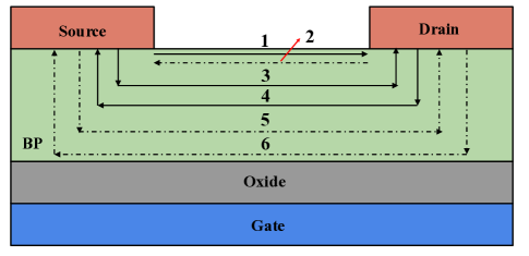
In Fig. 1, path 1 for electrons and path 2 for holes are transparent for all values of when 0. For 0, 0, and , paths labeled as and are unavailable for electron conduction. Likewise for hole, paths labeled as and are cut-off. Hence, we can conclude that for , the only way carriers can be transported between the contacts is through the paths labeled as 1 and 2 in Fig. 1. Results of this discussion are summarized in Table 1.
| Carrier | From | To | Path | Possibility |
|---|---|---|---|---|
| Electron | Source | Drain | 1 | ✓ |
| Electron | Source | Drain | 3 | ✗ |
| Electron | Drain | Source | 4 | ✗ |
| Hole | Drain | Source | 2 | ✓ |
| Hole | Source | Drain | 5 | ✗ |
| Hole | Drain | Source | 6 | ✗ |
Next, we consider the case when , , and . In this case, in addition to paths labeled as 1 and 2 in Fig. 1, there exist path for electron conduction and path for hole conduction. Results are summarized in Table 2.
| Carrier | From | To | Path | Possibility |
|---|---|---|---|---|
| Electron | Source | Drain | 1 | ✓ |
| Electron | Source | Drain | 3 | ✓ |
| Electron | Drain | Source | 4 | ✗ |
| Hole | Drain | Source | 2 | ✓ |
| Hole | Source | Drain | 5 | ✗ |
| Hole | Drain | Source | 6 | ✓ |
An appropriate bias-dependent model of the SB contact resistance in BP FETs must comprehend the distinct behavior for and regimes of transport when and . When and the possible carrier transport paths are the same as the results of the Table 1. Note that the bias dependence of SB contact resistance is exacerbated for hole conduction. This is because of the use of Ti as the metal contact in the experimental BP FET devices examined here. Compared to metals, such as Pd or Ni, Ti has a much lower work-function, which gives rise to a larger SB height and, therefore, large contact resistance values. Das et al. (2014); Haratipour et al. (2017) Also, the effect of contact resistance corresponding to hole conduction becomes especially significant in short channel devices in which the contact resistance could easily dominate the total drain-source resistance, limiting the maximum available current through the device. Valletta et al. (2011) Here, we assume that is a bias-independent, linear resistance. This is justified because of the p-type background doping in the devices under study.
The hole branch contact resistance assuming both ohmic resistance and the formation of the SB barrier at the metal/BP interface is given as
| (9) |
where
In the above set of equations, we use the logistic function to model the drain-bias dependence of various parameters. This function is similar to the / logistic function used in Eq. (6b) and is given as
| (10) |
where is used to adjust the sharpness of transition between two different bias regions, and is the drain-gate voltage at which additional paths for current conduction between the contacts are introduced (see Fig. 1 and the discussion.) This voltage is given as
| (11) |
where and are fitting parameters, and is given in Eq. (6bb). The model for described here captures the exponential dependence on as expected for SB contacts. Moreover, the model can also explain the drain-bias dependence of the contact resistance, following the discussion pertinent to Fig. 1. The contact resistance model introduces 10 parameters: , , , , , , , , , . The methodology to extract the contact resistance parameters from experimental data is presented in Appendix A.
III Effect of temperature
The main model parameters that are affected by temperature include the mobility, saturation velocity, non-ideality factor, and threshold voltage. Below we discuss the models to capture the temperature dependence of the various parameters.
Mobility:
Experimentally measured mobility of carriers in 2D materials is generally much lower than that predicted theoretically based on phonon-dominated collision. Mobility degradation in 2D materials results from defects and charged impurities at room temperature.Ong et al. (2014); Jariwala et al. (2014); Radisavljevic and Kis (2013); Ovchinnikov et al. (2014) Previous published works indicate that the mobility of carriers in BP follows a power law relationship with respect to temperature (). That is, for 100 K Ong et al. (2014); Trushkov and Perebeinos (2017); Li et al. (2014); Xia et al. (2014b) with typically in the range of -0.4 to 1.2 based on the type and concentration of carriers, BP crystal orientation, and the dielectric environment of the sample.Ong et al. (2014) In this paper, we use a constant carrier mobility model with temperature dependence given as
| (12) |
Here, is the value of the mobility of carriers at 298 K. As a result of the weakened polarization charge screening for oxides with a high dielectric constant, such as HfO2, we expect the temperature dependence of mobility in BP devices under study to be weak. Ong et al. (2014) As such, is expected to be in the range of 0.01 to 0.3.
The effect of carrier concentration on mobility, as demonstrated in recent experimental work,Haratipour et al. (2018) is studied in Appendix B. However, for validation of the model against experimental data, we consider a constant carrier mobility model as in the equation above. This allows us to restrict the number of model parameters without compromising the quality of the model fits while also providing reasonable estimates of extracted parameters (see Sec. IV on results.)
Saturation velocity:
The saturation velocity of carriers in BP is expected to decrease with an increase in temperature due to enhanced phonon-dominated scatterings. Chen et al. (2018) Here, we model of both electrons and holes using a linear equation in the range of 180 K to 298 K. This model is similar to that used previously. Chen et al. (2018)
| (13) |
where is the saturation velocity of carriers at 298 K, and is the temperature coefficient of saturation velocity. Typical value of is in the range of to m/sK.
Non-ideality factor:
At low , sub-threshold slope is modeled as where is the non-ideality factor defined previously as . Experimental results in Section IV indicate that for low-, is linearly proportional to temperature, Haratipour et al. (2016) implying that is independent of temperature. At high , tunneling current through the drain contact dominates, and the dependence of on temperature becomes sub-linear. This behavior can be reproduced by considering a linear temperature variation in the punch-through factor, :
| (14) |
where is the value of punch-through factor at 298 K, and captures the temperature sensitivity of . Typical values of are in the range of 0.009 to 0.025 1/VK.
Threshold voltage:
The temperature dependence of threshold voltage is introduced in the parameter used in Eq. (7) according to
| (15) |
is the value of the parameter at 298 K, and captures the temperature dependence of and it is on the order of . The linear variation of with temperature reproduces experimental and numerical results accurately as discussed in Section IV.
IV Results
The analytic I-V model developed here has 39 parameters, out of which 20 (11) parameters correspond to hole (electron) conduction, and 8 parameters (4 parameters for each carrier type) model the temperature sensitivity of current conduction. These models can be obtained through a systematic experimental validation methodology as explained in Appendix A.
There are four datasets available from experimental measurements and numerical simulation using the TCAD simulation tool Sentaurus from Synopsys.Guide (2016) The first two datasets correspond to the back-gated BP FETs with Schottky source/drain contacts which are fabricated at the University of Minnesota. In these two datasets, the BP flakes are exfoliated from the bulk crystal and transferred onto the local back gates. The gate dielectric is HfO2 with a thickness of 15 nm, and the gate metal is Ti(10 nm)/Pd(40 nm). The source and drain contacts are Ti (10 nm)/Au (90 nm). The device is passivated using 20-30 nm of Al2O3 to protect BP from atmospheric degradation. Additional fabrication details are given in Ref. Haratipour et al., 2016. The third and fourth dataset are obtained numerically by simulating top and back-gated BP FETs with Schottky source/drain contacts to show model validity for both FETs structures. Model parameters extracted for all datasets are listed in Tables 3 and 4.
For all datasets that are discussed in this section, we refer to the terminal that is grounded as the source terminal ( 0 V) and the drain terminal is biased at negative voltages (0 V). Note that this terminology of labeling the source/drain contacts is different from that followed conventionally, but it does not impact the interpretation of the model and the results. The implementation of the model in Verilog-A, SPICE circuit simulations, and Gummel symmetry test are presented in Appendix D.
Dataset 1: m, m, nm, nm, with rotational angle , and K
Dataset 1: m, m, nm, nm, with rotational angle at different temperatures.
Dataset 1: m, m, nm, nm, with rotational angle
Dataset 2: m, m, nm, nm, with rotational angle of .
Dataset 2: m, m, nm, nm, with rotational angle of , and K.
Dataset 2: m, m, nm, nm, with rotational angle of .
Dataset 3: m, m, nm, nm, nm, m, and K
Dataset 3: m, m, nm, nm, nm, and m.
| Dataset 1 | Dataset 2 | |||
| Model parameter | Electron | Hole | Electron | Hole |
| Carrier mobility at 298 K, (cm2/Vs) | 19 | 49 | 40 | 60 |
| Temperature dependence for mobility, (unit-less) | 0.01 | 0.17 | 0.2 | 0.3 |
| Carrier saturation velocity at 298 K, (m/s) | ||||
| Temperature dependence for saturation velocity, (m/sK) | 50 | 50 | 50 | 50 |
| Non-ideality factor, (unit-less) | 7 | 7.5 | 5.4 | 2.5 |
| Punch-through factor at 298 K, (1/V) | 0.12 | 3.42 | 3 | 3.5 |
| Temperature dependence for punch-through factor, (1/VK) | 0.025 | 0.02 | 0.009 | 0.013 |
| Shift in threshold voltage for charge trapping at 298 K, (V) | 0.67 | 1.02 | 1.02 | 0.71 |
| Temperature dependence for , (V/K) | 0 | |||
| Shift in ambipolar point at high , (1/V) | 0.14 | 0.52 | 1.05 | 0.79 |
| Threshold voltage adjustment parameter at high , | 0.002 | 0.083 | 0.4 | 0.28 |
| Ambipolar point at , (V) | 0.162 | 0.162 | 0.181 | 0.181 |
| Adjustment the smoothness of transition, (unit-less) | 9 | 9 | 4 | 6 |
| Shift in the in sub-threshold and strong inversion, (unit-less) | 3 | 3 | 2 | 6 |
| Empirical parameter for , (unit-less) | 1.5 | 1.5 | 1.5 | 2 |
| Contact resistance at 298 K, (-m) | — | |||
| Contact ohmic resistance, (-m) | — | — | — | () |
| Schottky barrier resistance coefficient, (-m) | — | — | — | 0.105(0.014) |
| Gate voltage dependence for Schottky barrier resistance, () | — | — | — | 2.053(1.39) |
| Transition point between two different transport paths, () | — | — | — | 0(0.452) |
| Adjustment the smoothness of , () | — | — | — | 0.67 |
| Dataset 3 | Dataset 4 | |||
| Model parameter | Electron | Hole | Electron | Hole |
| Carrier mobility at 298 K, () | 110 | 145 | 110 | 145 |
| Temperature dependence for mobility, (unit-less) | 0.05 | 0.15 | — | — |
| Carrier saturation velocity at 298 K, () | ||||
| Temperature dependence for saturation velocity, () | 50 | 50 | — | — |
| Non-ideality factor, (unit-less) | 2.5 | 2.5 | 6 | 3 |
| Punch-through factor at 298 K, () | 2.5 | 1 | 3 | 1 |
| Temperature dependence for punch-through factor, () | 0.0152 | 0.016 | — | — |
| Shift in threshold voltage for charge trapping at 298 K, () | 0.69 | 0.73 | 2 | 1 |
| Temperature dependence for , () | — | — | ||
| Shift in ambipolar point at high , () | 0.62 | 0.37 | 0.59 | 0.6 |
| Threshold voltage adjustment parameter at high , (1/V2) | 0.2 | 0.105 | 0.1 | 0.5 |
| Ambipolar point at , (V) | 0.02 | 0.02 | 0.17 | 0.17 |
| Adjustment the smoothness of transition, (unit-less) | 3.9 | 9 | 4 | 11 |
| Shift in the in sub-threshold and strong inversion, (unit-less) | 2 | 5 | 2 | 5 |
| Empirical parameter for , (unit-less) | 2 | 2 | 2 | 2 |
| Contact resistance at 298 K, (m) | — | |||
| Contact ohmic resistance, (m) | — | — | — | |
| Schottky barrier resistance coefficient, (m) | — | — | — | 0.183(0) |
| Gate voltage dependence for Schottky barrier resistance, () | — | — | — | 6(—) |
| Transition point between two different transport paths, () | — | — | — | 0(2) |
| Adjustment the smoothness of , () | — | — | — | 0.17 |
IV.1 Dataset 1
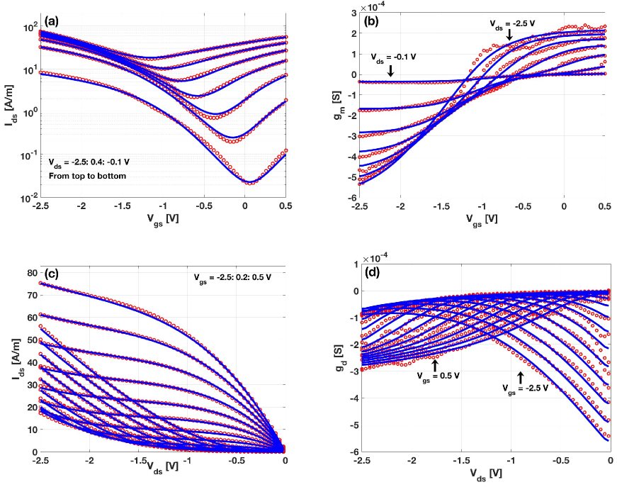
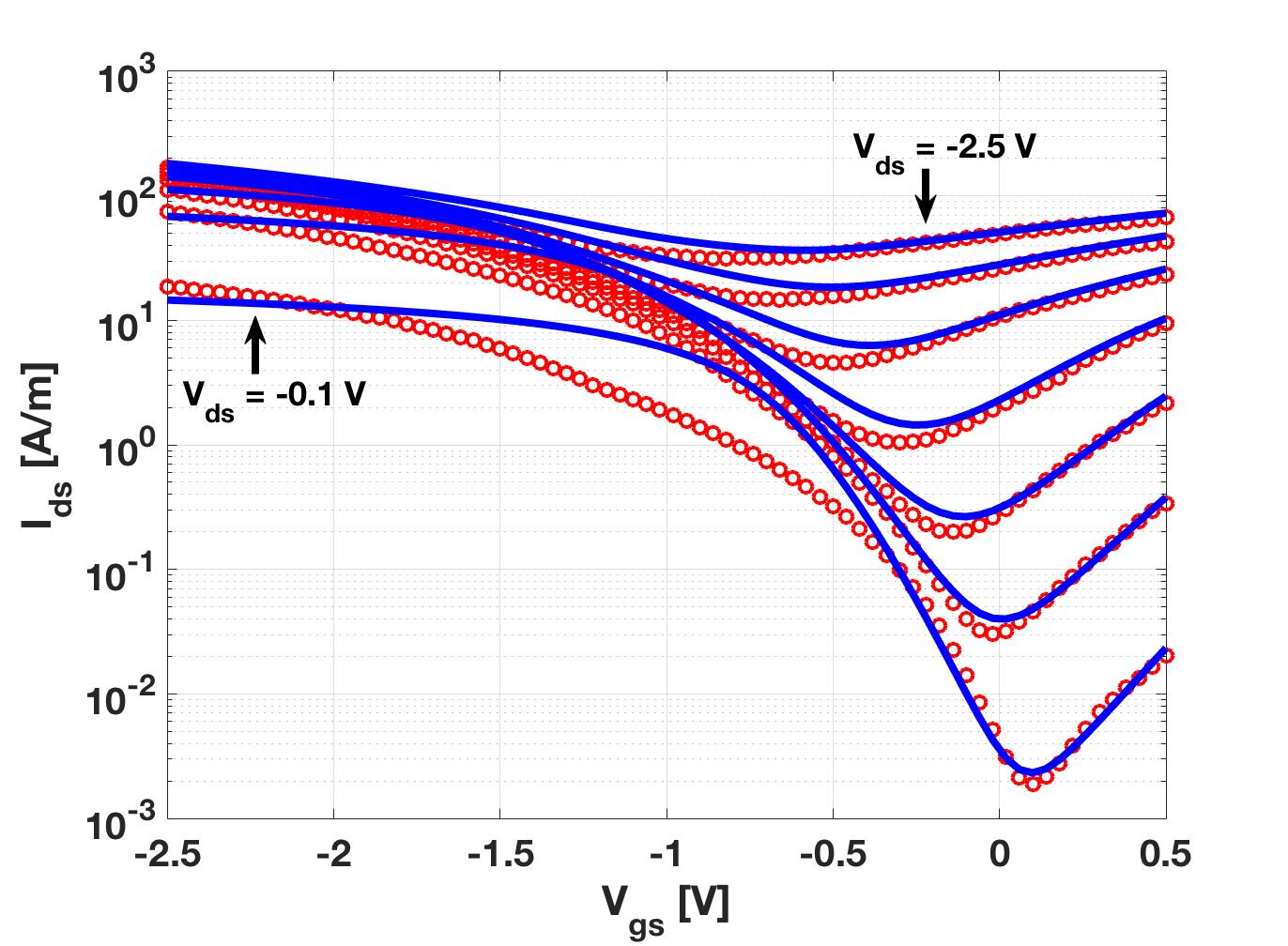
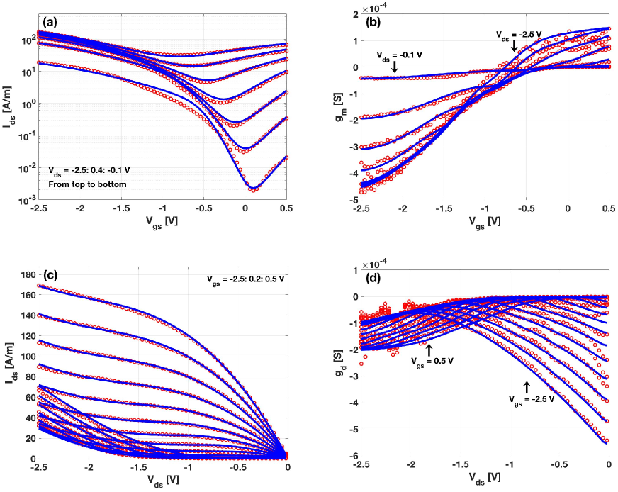
Dataset 1 corresponds to back-gated BP FETs with m, m, nm, nm, with rotational angle (rotational angle is defined along the zigzag direction and is along the armchair direction.) Model fits to experimental transfer curves (-) and transconductance () for a broad range of values at 298 K are shown in Figs. 2 (a) and (b). Figures 2 (c) and (d) show the model fits to measured output curves (-) and output conductance () for a broad range of values at 298 K. The model provides an excellent fit to the measured data and has the required smoothness of current derivatives as expected of compact models. The maximum output current in this dataset is less than 100 A/m obtained at = -2.5 V. Due to its limited on-current, the effect of contact resistance is not discernible. As such, we are able to fit measured data with negligible contact resistance. Neglecting the contact resistance also allows us to extract values of carrier mobility and velocity that are within the expected range for this set of BP FETs.
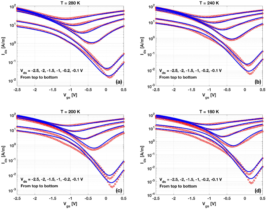
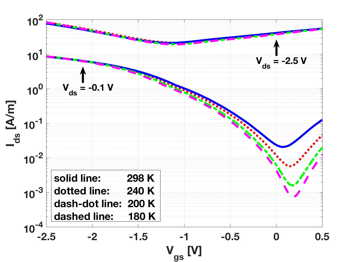
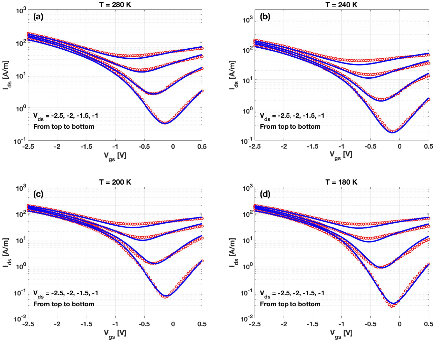
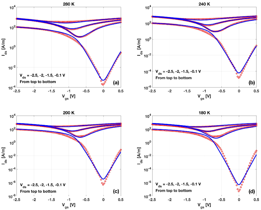
We further validate this dataset using the model at 280 K, 240 K, 200 K, and 180 K. Results are shown in Fig. 3. For all temperatures considered here, the maximum measured current stays under 100 A/m, which can be explained by neglecting the contact resistances. The slight increase in on-current with a reduction in temperature is due to the increase in carrier saturation velocity. The dependence of on temperature for this dataset is examined in Fig. 4. This figure shows that at low , decreases at lower temperature, while at high , is nearly independent of temperature. Hence, the assumption that is independent of temperature and that varies linearly with temperature (Eq. (14)) is justified.
IV.2 Dataset 2
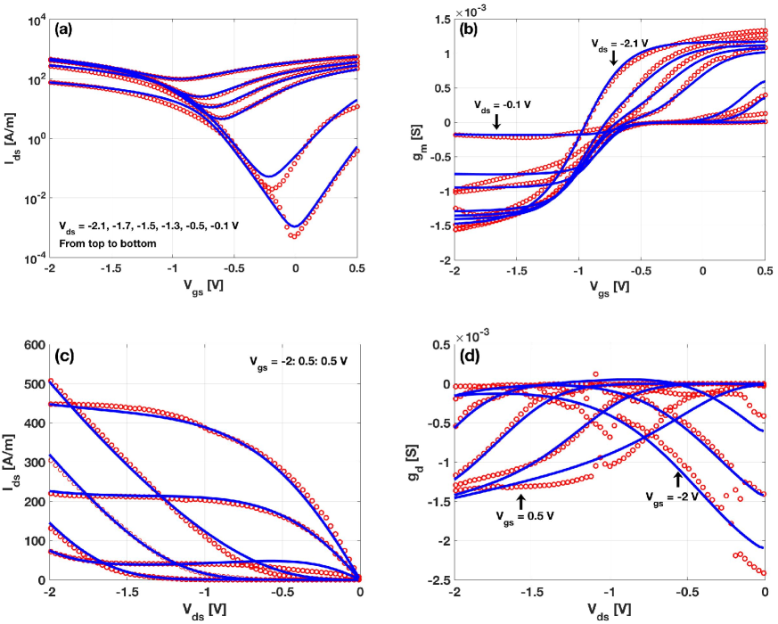
The second dataset corresponds to back-gated BP FETs with m, m, nm, nm, and rotational angle of . Unlike dataset 1, where the effect of contact resistances is not evident due to the low on-current of the device, a proper consideration of contact resistances is required to interpret dataset 2. This is because the channel length of the device in dataset 2 is smaller than that of the device analyzed in dataset 1. Assuming a constant value for = 21 m, the fit of the model to measured data is shown in Fig. 5. The figure clearly shows that a constant is inadequate to explain the experimental data. A higher value of for V and a lower value of for V can significantly improve the fit quality. Therefore, a bias-dependent nonlinear model of is necessitated in this case as discussed in Sec. II.2.
Model fits to the experimental I-V, transconductance, and output conductance data for the dataset 2 are shown in Figs. 6 (a)-(d). Model parameters extracted from this fit are listed in Table 3. The validation of the model at various temperatures 280, 240, 200, and 180 K for dataset 2 is shown in Fig. 7. Because of the lack of experimental data at low temperatures, we only focus on V. The model provides an excellent match with experimental data over broad bias and temperature range for this device.
IV.3 Datasets 3 and 4
The last two datasets are obtained through numerical simulations using the TCAD tool Sentaurus for top-gated and back-gated BP FETs with channel length m, m, nm, top-oxide thickness, = 10 nm and back-oxide thickness nm, and source/drain contact length, m. In Sentaurus, the Poisson and current continuity equations are solved self-consistently for both the contact and channel regions under the drift-diffusion approximation. Since Sentaurus does not provide parameters for 2D materials, we use previously published results obtained from experimental and theoretical calculations summarized in table 5. Haratipour et al. (2016); Penumatcha et al. (2015); Qiao et al. (2014) The Schottky contact is defined as a boundary condition between the contacts and the semiconductor. The work function of the metal contact is chosen as eV, and the electron affinity of BP is eV. Haratipour et al. (2016) Besides the thermionic emission, thermally assisted and direct tunneling through the SB are also considered using a non-local tunneling model. Arutchelvan et al. (2017) In this simulation, we ignore the effects of traps and carriers generation and recombination.
Model fits to the numerical I-V, transconductance, and output conductance data for the dataset 3 are shown in Figs. 8 (a)-(d). Model fits corresponding to dataset 4 also shown an excellent agreement with the data, but are omitted for brevity. Model parameters extracted from this fit are listed in Table 4. Also, the validation of the model at various temperatures 280 K, 240 K, 200 K, and 180 K for dataset 3 is shown in Fig. 9. The model accurately predicts the I-V characteristics over broad bias and temperature range for this dataset. The main difference between the top- and back-gated structures is that the contact resistances are linear in the top-gated structure. This is because the transport path for carriers does not depend on the applied bias (see Appendix C for details.)
| Band gap (eV) | 0.69 |
|---|---|
| Electron effective mass (unit-less) | 0.15 (armchair direction) |
| 1.18 (zigzag direction) | |
| Hole effective mass (unit-less) | 0.14 (armchair direction) |
| 0.89 (zigzag direction) | |
| Dielectric constant (unit-less) | 8.3 |
| Electron affinity (eV) | 3.655 |
For all datasets, we observe that , which is in agreement with experimental results previously reported in various BP FETs.Liu et al. (2015); Haratipour et al. (2016); Qiao et al. (2014); Chen et al. (2017) The extracted values of carrier mobility, unfortunately, are notably smaller than those reported in prior work.Li et al. (2014); Liu et al. (2014); Qiao et al. (2014); Xia et al. (2014b) Yet, the mobility values of these devices are very close to those extracted from measurements of similar devices fabricated at the University of Minnesota. Haratipour and Koester (2016); Haratipour et al. (2015) The reason for low mobility values in these samples is attributed to a combination of interface scattering, remote phonon scattering from the gate dielectric and the substrate, defects, and charged impurity scattering. Ong et al. (2014); Haratipour et al. (2015)However, recent experimental work has demonstrated that the carrier mobility in back-gated BP FETs with HfO2 dielectric can be improved to 165 at room-temperature by optimizing the fabrication method.Haratipour et al. (2018) The extracted values of the saturation velocity of carriers are also in agreement with those reported in prior work.Chen et al. (2018); Chandrasekar et al. (2016); Zhu et al. (2016) As a result of the large effective mass of electrons in BP, the model correctly predicts that . Chen et al. (2018)
V Conclusion
In this work, we develop a virtual-source-based analytic model to describe ambipolar current conduction in BP transistors over a broad range of bias and temperature values. The model comprehends the nonlinearity and the bias-dependence of Schottky source/drain contacts, which is necessary to explain the I-V behavior of short-channel back-gated BP transistors. The model can also capture the low-temperature transport in BP transistors. To accomplish this, key parameters such as the carrier mobility, saturation velocity, punch-through factor, and threshold voltage are modeled as simple temperature-dependent functions. The accuracy of the model is demonstrated by applying to top- and back-gated BP transistors with channel lengths of 1000 nm and 300 nm with temperature from 300 K to 180 K. The smoothness of the current and its derivatives is guaranteed in the model, thus satisfying a key criteria for compact models. Since the model is based on threshold-voltage-based current calculation, it does not require a self-consistent solution based on surface potential. As such, the model is computationally less expensive and suitable to simulate and optimize BP-based circuits.
VI ACKNOWLEDGMENTS
Elahe Yarmoghaddam and Shaloo Rakheja acknowledge the funding support of National Science Foundation (NSF) through the grant no. CCF1565656. S. Rakheja also acknowledges the funding support of NYU Wireless through the Infistrial Affiliates Program. Nazila Haratipour and Steven J. Koester acknowledge primary support from NSF through the University of Minnesota MRSEC under Award DMR-1420013.
Appendix A Extraction methodology of model parameters
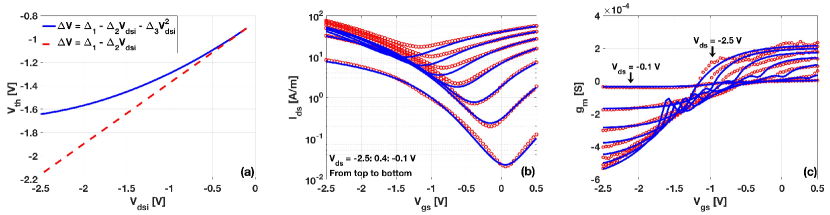
The parameter extraction begins by identifying the Dirac point (minimum conductivity), , at = 0 V. The values of , , and are determined by matching the Dirac point from experimentally measured transfer curves and the model at all values. As shown in Fig. 2(a) in Sec. IVA, the Dirac point voltage is a strong function of which varies from V for V to V for V.
The on-off current ratio is about at V. However, the on-off current ratio is as low as 4 at V. This implies that the device is nearly always on at high . This behavior can be explained by observing that even when the current due to hole conduction drops, the electron branch current increases, preventing the device from turning off at high . By using an appropriate model of the electron and hole threshold voltages as in Eq. 7, we can capture the on-off device behavior in both equilibrium and off-equilibrium transport conditions. With (positive value), we can model the decrease (increase) in at large negative values. Figure. 10(a) plots the hole threshold voltage () predicted by the model for the first dataset as a function of for (solid line), and (dashed line). With , we see that monotonically decreases with , which is not the desired behavior. The transfer characteristics of the device using and other parameters as listed in Table 3 are plotted in Fig. 10(b). The figure shows a poor match between the model and experimental data at highly negative .
The transfer curve experimental data is used to obtain the values of the non-ideality factor () at = 0 V. Similarly, the punch-through factor () can be obtained from experimental data by measuring the sub-threshold slope (SS) at various values. Moreover, the effective mobility values of these devices are chosen very close to those extracted from measurements of similar devices fabricated at the University of Minnesota. Haratipour and Koester (2016); Haratipour et al. (2015) The extracted values of the saturation velocity of carriers are also in agreement with those reported in prior work.Chen et al. (2018); Chandrasekar et al. (2016); Zhu et al. (2016)
In this model, and are empirical fitting parameters, and according to previous published works for VS model, Li and Rakheja (2018); Khakifirooz et al. (2009); Rakheja et al. (2014) their values are tuned within a range of to and to , respectively. Prior VS models have shown that the parameter is of the same order of magnitude as . Figure 10 (c) shows the transconductance of dataset 1 by using , which is the typical value of in prior VS models. All other fitting parameters are the same as those listed in Table 3. This figure shows that for , the transconductance displays several kinks, which can be smoothed by using a slightly larger value of as listed in Table 3.
The value of is obtained using TLM measurements reported in Refs. Haratipour et al., 2017, 2015. The process to find optimal parameters in , which is non-linear and bias-dependent, is as follows. First, we choose a large negative value of such that the term (see Eq. (9)). This allows us to extract appropriate values of and using the measured output characteristics. On the other hand, at very low , in Eq. (9) approaches unity. Using experimental I-V data in this regime, we can identify the value of . The parameters and are empirical in nature and extracted by minimizing the least-square error between the model and experimental I-V data. Finally, we use the I-V measurements at different temperatures to identify the temperature dependence of key model parameters, namely mobility, saturation velocity, punch-through factor, and threshold voltage. The extracted temperature coefficients lie in the expected range based on previous experimental and theoretical predictions.
Dataset1: m, m, nm, nm, with rotational angle , and K
Appendix B Carrier concentration dependent mobility model
In recent experimental work, the effect of carrier concentration on both hole and electron mobility in back-gated BP FETs was explored over a broad range of temperatures.Haratipour et al. (2018) As a result of electrostatic screening in the sample, the carrier mobility was found to increase with an increase in carrier concentration for all temperatures ranging from 77 K to 295 K. To handle the variation in carrier mobility with carrier concentration, Eq.(12) is modified as
| (16) |
where , , and are fitting parameters depending on the oxide dielectric constant, BP crystal orientation, and impurity density,Ma and Jena (2014) is also given in Eq. 4b.
The updated model introduces an additional three fitting parameters, which can be determined from measurement data such as in Ref. 50. Model parameters corresponding to dataset 2 at 298 K are extracted using Eq.16 for the hole mobility. The fitting results are shown in Fig. 11. Here, only the parameters corresponding to the contact resistances (, , and ), shift in threshold voltage (), and empirical parameter are tweaked, while the remainder model parameters are the same as those reported in Table 3. With a positive value of , the carrier mobility increases at higher (higher carrier concentration), necessitating a slightly larger value of the hole contact resistance to match the experimental data in on-state.
Dataset 2: m, m, nm, nm, with rotational angle of

Appendix C Electrostatic potential and contact resistances
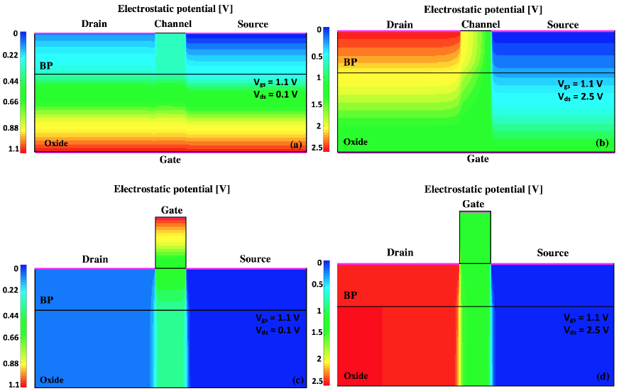
To understand the nonlinearity of contact resistances, we consider the data obtained from numerical simulations using Synopsys Sentaurus (datasets 3 and 4 in the main text). In Fig. 12, electrostatic potential distribution for , = 0.1 V and 2.5 V is shown. Results in Fig. 12(a) and (b) show that the carriers paths between the source/drain contacts depend on the applied bias voltages for the back-gated device. This is in agreement with the discussion in Sec. II.2. For , only paths 1 and 2 labeled in Fig. 1 are transparent for current conduction. However, additional conduction paths for both carrier types contribute to current when . On the other hand, for top-gated structure, as shown in Figs. 12(c) and (d), carrier transport is independent of the bias voltages.
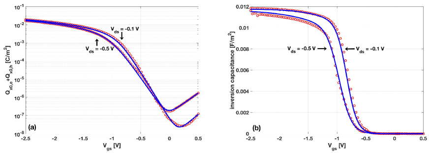
The analytic charge model (Eq. 4b in Sec. IIA) is validated by comparing the results against the charges obtained numerically for dataset 4. Results are shown in Fig. 13. The model also faithfully reproduces the behavior of inversion capacitance (-) versus , thus validating our charge modeling approach.
Numerical simulation: m, m, nm, nm, and contact length m.
Appendix D Verilog-A and circuit simulation
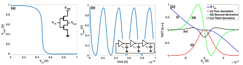
The model is implemented in Verilog-A to perform circuit simulations in SPICE. In Fig. 14, the model is used to simulate the dc behavior of a BP-based inverter and the transient behavior of a BP-based 3-stage ring oscillator circuit. Transistor parameters corresponding to dataset 2 are used for these simulations. The results show the mathematical robustness of the model, ease of computation, and the capability to handle large-scale circuit simulations.
The model developed in this paper also satisfies the Gummel symmetry test (GST) required for physically accurate and well-behaved compact models. According to the GST, the model must have a symmetric formulation around V. Additionally, the higher order derivatives of current must be continuous. Radhakrishna (2016) To demonstrate that the model passes the GST, the source and drain are biased differentially ( and ), while the gate terminal has a fixed voltage. Results of the GST reported in Fig. 14 (c) verify that the model and its higher order derivatives are symmetric around V.
References
- Yarmoghaddam and Rakheja (2017) E. Yarmoghaddam and S. Rakheja, Journal of Applied Physics 122, 083101 (2017).
- Rakheja et al. (2013a) S. Rakheja, V. Kumar, and A. Naeemi, Proceedings of the IEEE 101, 1740 (2013a).
- Novoselov et al. (2005) K. S. Novoselov, A. K. Geim, S. Morozov, D. Jiang, M. Katsnelson, I. Grigorieva, S. Dubonos, Firsov, and AA, nature 438, 197 (2005).
- Wang et al. (2012) Q. H. Wang, K. Kalantar-Zadeh, A. Kis, J. N. Coleman, and M. S. Strano, Nature nanotechnology 7, 699 (2012).
- Fivaz and Mooser (1967) R. Fivaz and E. Mooser, Physical Review 163, 743 (1967).
- Houssa et al. (2011) M. Houssa, E. Scalise, K. Sankaran, G. Pourtois, V. Afanas’ Ev, and A. Stesmans, Applied Physics Letters 98, 223107 (2011).
- Vogt et al. (2012) P. Vogt, P. De Padova, C. Quaresima, J. Avila, E. Frantzeskakis, M. C. Asensio, A. Resta, B. Ealet, and G. Le Lay, Physical review letters 108, 155501 (2012).
- Bianco et al. (2013) E. Bianco, S. Butler, S. Jiang, O. D. Restrepo, W. Windl, and J. E. Goldberger, Acs Nano 7, 4414 (2013).
- Xia et al. (2014a) F. Xia, H. Wang, D. Xiao, M. Dubey, and A. Ramasubramaniam, Nature Photonics 8, 899 (2014a).
- Das et al. (2014) S. Das, M. Demarteau, and A. Roelofs, ACS nano 8, 11730 (2014).
- Yi et al. (2017) Y. Yi, X.-F. Yu, W. Zhou, J. Wang, and P. K. Chu, Materials Science and Engineering: R: Reports 120, 1 (2017).
- Qiao et al. (2014) J. Qiao, X. Kong, Z.-X. Hu, F. Yang, and W. Ji, Nature communications 5, 4475 (2014).
- Geim and Novoselov (2007) A. K. Geim and K. S. Novoselov, Nature materials 6, 183 (2007).
- Hwang and Sarma (2008) E. Hwang and S. D. Sarma, Physical Review B 77, 115449 (2008).
- Han et al. (2014) X. Han, H. M. Stewart, S. A. Shevlin, C. R. A. Catlow, and Z. X. Guo, Nano letters 14, 4607 (2014).
- Du et al. (2014) Y. Du, H. Liu, Y. Deng, and P. D. Ye, ACS nano 8, 10035 (2014).
- Huang et al. (2017) H. Huang, Q. Xiao, J. Wang, X.-F. Yu, H. Wang, H. Zhang, and P. K. Chu, npj 2D Materials and Applications 1, 20 (2017).
- Haratipour et al. (2016) N. Haratipour, S. Namgung, S.-H. Oh, and S. J. Koester, ACS nano 10, 3791 (2016).
- Yang et al. (2016) L. Yang, G. Qiu, M. Si, A. Charnas, C. Milligan, D. Zemlyanov, H. Zhou, Y. Du, Y. Lin, W. Tsai, et al., in Electron Devices Meeting (IEDM), 2016 IEEE International (IEEE, 2016), pp. 5–5.
- Bohloul et al. (2016) S. Bohloul, L. Zhang, K. Gong, and H. Guo, Applied Physics Letters 108, 033508 (2016).
- Luo et al. (2015) Z. Luo, J. Maassen, Y. Deng, Y. Du, R. P. Garrelts, M. S. Lundstrom, D. Y. Peide, and X. Xu, Nature communications 6, 8572 (2015).
- Xia et al. (2014b) F. Xia, H. Wang, and Y. Jia, Nature communications 5, 4458 (2014b).
- Rakheja et al. (2014) S. Rakheja, Y. Wu, H. Wang, T. Palacios, P. Avouris, and D. A. Antoniadis, IEEE Transactions on Nanotechnology 13, 1005 (2014).
- Penumatcha et al. (2015) A. V. Penumatcha, R. B. Salazar, and J. Appenzeller, Nature communications 6, 8948 (2015).
- Esqueda et al. (2017) I. S. Esqueda, H. Tian, X. Yan, and H. Wang, IEEE Transactions on Electron Devices 64, 5163 (2017).
- Wang et al. (2016) L. Wang, S. Peng, W. Wang, G. Xu, Z. Ji, N. Lu, L. Li, Z. Jin, and M. Liu, Journal of Applied Physics 120, 084509 (2016).
- Wang et al. (2017) L. Wang, Y. Li, X. Feng, K.-W. Ang, X. Gong, A. Thean, and G. Liang, in Electron Devices Meeting (IEDM), 2017 IEEE International (IEEE, 2017), pp. 31–4.
- Cao et al. (2018) J. Cao, S. Peng, W. Liu, Q. Wu, L. Li, D. Geng, G. Yang, Z. Ji, N. Lu, and M. Liu, Journal of Applied Physics 123, 064501 (2018).
- Taur et al. (2016) Y. Taur, J. Wu, and J. Min, IEEE Transactions on Electron Devices 63, 2550 (2016).
- Marin et al. (2018) E. G. Marin, S. J. Bader, and D. Jena, IEEE Transactions on Electron Devices 65, 1239 (2018).
- Landauer (1957) R. Landauer, IBM Journal of Research and Development 1, 223 (1957).
- Datta (1997) S. Datta, Electronic transport in mesoscopic systems (Cambridge university press, 1997).
- Lundstrom and Antoniadis (2014) M. S. Lundstrom and D. A. Antoniadis, IEEE Transactions on Electron Devices 61, 225 (2014).
- Radhakrishna et al. (2014) U. Radhakrishna, T. Imada, T. Palacios, and D. Antoniadis, physica status solidi (c) 11, 848 (2014).
- Rakheja et al. (2013b) S. Rakheja, H. Wang, T. Palacios, I. Meric, K. Shepard, and D. Antoniadis, in Electron Devices Meeting (IEDM), 2013 IEEE International (IEEE, 2013b), pp. 5–5.
- Haratipour et al. (2015) N. Haratipour, M. C. Robbins, and S. J. Koester, in Device Research Conference (DRC), 2015 73rd Annual (IEEE, 2015), pp. 243–244.
- Haratipour and Koester (2016) N. Haratipour and S. J. Koester, IEEE Electron Device Letters 37, 103 (2016).
- Chang et al. (2014) H.-Y. Chang, W. Zhu, and D. Akinwande, Applied Physics Letters 104, 113504 (2014).
- Chang et al. (2017) H.-M. Chang, A. Charnas, Y.-M. Lin, D. Y. Peide, C.-I. Wu, and C.-H. Wu, Scientific reports 7, 16857 (2017).
- Du et al. (2016) Y. Du, A. T. Neal, H. Zhou, and D. Y. Peide, Journal of Physics: Condensed Matter 28, 263002 (2016).
- Xu et al. (2016) Y. Xu, C. Cheng, S. Du, J. Yang, B. Yu, J. Luo, W. Yin, E. Li, S. Dong, P. Ye, et al., ACS nano 10, 4895 (2016).
- Haratipour et al. (2017) N. Haratipour, S. Namgung, R. Grassi, T. Low, S.-H. Oh, and S. J. Koester, IEEE Electron Device Letters 38, 685 (2017).
- Valletta et al. (2011) A. Valletta, A. Daami, M. Benwadih, R. Coppard, G. Fortunato, M. Rapisarda, F. Torricelli, and L. Mariucci, Applied Physics Letters 99, 271 (2011).
- Ong et al. (2014) Z.-Y. Ong, G. Zhang, and Y. W. Zhang, Journal of Applied Physics 116, 214505 (2014).
- Jariwala et al. (2014) D. Jariwala, V. K. Sangwan, L. J. Lauhon, T. J. Marks, and M. C. Hersam, ACS nano 8, 1102 (2014).
- Radisavljevic and Kis (2013) B. Radisavljevic and A. Kis, Nature materials 12, 815 (2013).
- Ovchinnikov et al. (2014) D. Ovchinnikov, A. Allain, Y.-S. Huang, D. Dumcenco, and A. Kis, ACS nano 8, 8174 (2014).
- Trushkov and Perebeinos (2017) Y. Trushkov and V. Perebeinos, Physical Review B 95, 075436 (2017).
- Li et al. (2014) L. Li, Y. Yu, G. J. Ye, Q. Ge, X. Ou, H. Wu, D. Feng, X. H. Chen, and Y. Zhang, Nature nanotechnology 9, 372 (2014).
- Haratipour et al. (2018) N. Haratipour, Y. Liu, R. J. Wu, S. Namgung, P. P. Ruden, K. A. Mkhoyan, S.-H. Oh, and S. J. Koester, IEEE Transactions on Electron Devices pp. 1–9 (2018).
- Chen et al. (2018) X. Chen, C. Chen, A. Levi, L. Houben, B. Deng, S. Yuan, C. Ma, K. Watanabe, T. Taniguchi, D. Naveh, et al., ACS nano 12, 5003 (2018).
- Guide (2016) S. D. U. Guide, Inc., Mountain View, CA (2016).
- Arutchelvan et al. (2017) G. Arutchelvan, C. J. L. de la Rosa, P. Matagne, S. Sutar, I. Radu, C. Huyghebaert, S. De Gendt, and M. Heyns, Nanoscale 9, 10869 (2017).
- Liu et al. (2015) H. Liu, Y. Du, Y. Deng, and D. Y. Peide, Chemical Society Reviews 44, 2732 (2015).
- Chen et al. (2017) P. Chen, N. Li, X. Chen, W.-J. Ong, and X. Zhao, 2D Materials 5, 014002 (2017).
- Liu et al. (2014) H. Liu, A. T. Neal, Z. Zhu, Z. Luo, X. Xu, D. Tománek, and P. D. Ye, ACS nano 8, 4033 (2014).
- Chandrasekar et al. (2016) H. Chandrasekar, K. L. Ganapathi, S. Bhattacharjee, N. Bhat, and D. N. Nath, IEEE Transactions on Electron Devices 63, 767 (2016).
- Zhu et al. (2016) W. Zhu, S. Park, M. N. Yogeesh, K. M. McNicholas, S. R. Bank, and D. Akinwande, Nano letters 16, 2301 (2016).
- Li and Rakheja (2018) K. Li and S. Rakheja, Journal of Applied Physics 123, 184501 (2018).
- Khakifirooz et al. (2009) A. Khakifirooz, O. M. Nayfeh, and D. Antoniadis, IEEE Transactions on Electron Devices 56, 1674 (2009).
- Ma and Jena (2014) N. Ma and D. Jena, Physical Review X 4, 011043 (2014).
- Radhakrishna (2016) U. Radhakrishna, Ph.D. thesis, Massachusetts Institute of Technology (2016).