Magnetic-field controlled anomalous refraction in doped semiconductors
Abstract
We predict here that a slab made of a doped semiconductor can exhibit anomalous refraction under the application of a static magnetic field. This anomalous refraction takes place in the far-infrared range and it occurs for any angle of incidence. We show that this effect is due to the fact that a doped semiconductor under a magnetic field can behave, to some extent, as a hyperbolic metamaterial. We also show that the occurrence of this anomalous refraction enables a semiconductor slab under a magnetic field to partially focus the electromagnetic radiation. The remarkable thing in our case is that we deal with naturally occurring materials and the anomalous refraction can be tuned at will with an external field.
I Introduction
Veselago’s proposal Veselago1968 of a negative refraction index triggered the design and fabrication of artificial materials, known as metamaterials, with peculiar optical properties Shalaev2007 . In principle, such materials were meant to possess an isotropic optical response, that is, their dielectric permittivity and magnetic permeability are given by scalar functions, being both negative in a certain frequency range. However, the experimental realization of these materials is usually carried out with an ensemble of building blocks, leading to anisotropic effective optical responses Pendry2004 ; Han2008 . A notable example of materials with engineered anisotropy are the hyperbolic metamaterials, which are uniaxial media described by a permittivity that is a diagonal tensor of the form: Poddubny2013 ; Ferrari2015 . These metamaterials are usually fabricated with the help of metal-dielectric multilayered structures or nanowire arrays Poddubny2013 ; Ferrari2015 . What makes special this class of metamaterials is the fact that for certain frequency ranges it holds that the real part of and have opposite signs. This, in turn, leads to the fact that the dispersion relation of the electromagnetic waves propagating inside these materials is hyperbolic, i.e., it adopts the following form
| (1) |
where is the frequency, is the speed of light, and are the corresponding components of the wave vector. As a consequence, these metamaterials are able to convert incoming evanescent waves into propagating ones. This special feature of hyperbolic metamaterials makes it possible their application for negative refraction devices, subwavelenght imaging and superlensing, and hyperbolic waveguides Poddubny2013 ; Ferrari2015 . In addition, they can exhibit anomalous refraction, which is the inversion of the transversal component of the Poynting vector once the electromagnetic wave enters into the medium Hu2002 .
In this work we explore the possibility to use a simple semiconductor to mimic the behavior of a hyperbolic metamaterial in the far-infrared range of the electromagnetic spectrum. In particular, we study the possibility to induce an anomalous refraction by simply applying a static magnetic field to a doped semiconductor. This idea was inspired by our recent work where we showed that, under certain circumstances, doped semiconductors can behave as hyperbolic near-field thermal emitters when subjected to an external magnetic field Moncada2015 . This led us to the question of whether semiconductors under magnetic fields can exhibit the defining properties of hyperbolic metamaterials in other contexts. As we show below, this is actually the case and we shall illustrate here this phenomenon with the case of a slab made of -doped indium antimonide (InSb), a semiconductor that has been amply studied in the context of magneto-plasmonics Palik1976 , near-field thermal radiation Moncada2015 ; Ben-Abdallah2016 ; Zhu2016 ; Abraham-Ekeroth2018 , magnetically controlled subwavelength resolution Cheng2015 , and in biosensing plataforms Sreekanth2016 . To be more precise, we show in this work that a slab of InSb in the presence of a magnetic field can exhibit anomalous refraction for any angle of incidence in a wide range of frequencies in the far-infrared We also predict that the occurrence of this anomalous refraction partially focus the electromagnetic radiation. The notable thing about this discovery is that this anomalous refraction only involves the use of a naturally occurring material and it is highly tunable with an external field.
The rest of the paper is organized as follows. In Sec. II, we present the system under study and briefly remind the basics of anomalous refraction. Section III is devoted to the description of the main results of the work. In particular, we present a detailed analysis of the anomalous refraction in a InSb slab subjected to a static magnetic field. In Sec. IV we explore the possibility of inducing partial focusing in a InSb slab with the application of an external magnetic field. The main conclusions of this work are briefly summarized in Sec. V. Finally, we present additional results in Appendix A to clarify some of the statements made in different sections.
II System and reminder of anomalous refraction
The system that we consider is a slab of thickness made of a doped semiconductor, see Fig. 1(a). The slab is surrounded by air (or vacuum) and we assume that there is a static magnetic field applied perpendicular to the slab’s surfaces, which is the -direction according to Fig. 1(a), i.e., . Because of the existence of free carriers in a doped semiconductor, it is well-known that the application of a magnetic field induces a magneto-optical activity that in our geometry can be generically described by the following permittivity tensor Palik1976 ; Zvezdin1997
| (2) |
The different elements in this tensor depend on the applied magnetic field and their exact form will be discussed in the next section. For the moment, the important thing to notice is that the diagonal part of this tensor has exactly the same form as in the case of a hyperbolic material. However, this tensor also has off-diagonal elements, which are absent in a uniaxial material and are induced by the applied field. These off-diagonal elements are responsible for the polarization conversion that an electromagnetic wave undergoes when it is reflected by the slab or transmitted through it. This is actually the basis of the Kerr and Faraday magneto-optical effects that are observed in these materials Zvezdin1997 .
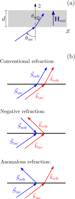
Our goal in this work is to analyze the transmission of a plane wave that impinges in this magneto-optical slab with a certain angle of incidence, . Here, we assume that the -plane coincides with the incidence plane. In particular, we want to find out whether the anomalous refraction can take place in the system under consideration, something that is not trivial a priori because of the presence of the off-diagonal terms in the permittivity tensor of Eq. (2). This problem will be analyzed in detail in the following section, but for didactic reasons we are going to assume in this section that we can ignore the off-diagonal elements in Eq. (2). This will allow us to remind the basics of the anomalous refraction and to explain how it comes about.
With the assumption that the permittivity tensor is diagonal, , it is easy to analyze the refraction of a plane wave by the slab Hu2002 . Considering first the case of transversal electric (TE) polarized waves , the solution of Maxwell’s equations lead to the following dispersion relation inside the slab
| (3) |
while the corresponding -component of the Poynting vector evaluated right inside the slab (after crossing the first interface) is given by
| (4) |
where is the vacuum permeability. Similarly, for transversal magnetic (TM) waves , one obtains the dispersion relation
| (5) |
and the -component of the Poynting vector right inside the slab
| (6) |
where is the vacuum permittivity. The condition for the anomalous refraction is a negative -component of the Poynting vector in the slab [c.f. Fig. 1(b)]. From Eq. (4), it is clear that is not possible to have anomalous refraction for an incident TE-polarized wave, while for TM-polarized waves this is possible provided that [see Eq. (6)]. If this condition is fulfilled, the dispersion relation of Eq. (5) requires in order to have propagating waves, instead of evanescent ones, inside the slab, as it can be seen from the expression for the -component of the wave vector:
| (7) |
Notice that according to this expression, the anomalous refraction within the uniaxial approximation occurs for any angle of incidence. This absence of a critical angle in this slab made of natural occurring MO materials differs from the behavior of uniaxial bianisotropic (artificial) metamaterials with permittivity and permeability Hu2002 .
Let us stress that the whole discussion above was based on the uniaxial approximation (with no off-diagonal elements of the permittivity tensor). In the next section, we investigate how these conclusions are modified by analyzing the exact results taking into account the full structure of the permittivity tensor in Eq. (2). We can anticipate that the conditions for the appearance of the anomalous refraction derived above remain valid in the case of a doped semiconductor under a magnetic field. This is actually due to the fact that the dispersion relations of the different propagating modes, see Eqs. (3) and (5), are not strongly modified by the off-diagonal elements. This is discussed in some detail in Appendix A. Let us also say that, on the contrary, the wave propagation inside the slab is clearly altered by the off-diagonal elements.
III Anomalous refraction in a doped semiconductor
In the previous section we have reminded that a hyperbolic metamaterial with a scalar permeability exhibits an anomalous refraction for any angle of incidence. Since a doped semiconductor is not quite a uniaxial material, see Eq. (2), it is not obvious a priori whether it can also exhibit this peculiar phenomenon. In order to clarify this issue, we investigate in this section the refraction through a slab made of -doped InSb. The optical properties of this material under a perpendicular magnetic field, see Fig. 1(a), are described by a permittivity tensor of the form of Eq. (2), where the different elements of that tensor are given by Palik1976
| (8) | |||||
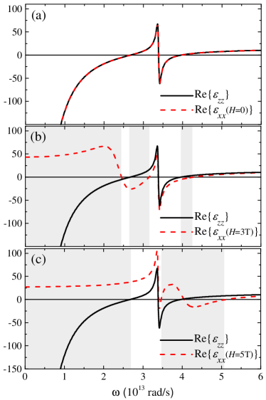
Here, is the high-frequency dielectric constant, is the longitudinal optical phonon frequency, is the transverse optical phonon frequency, defines the plasma frequency of free carriers of density and effective mass , is the phonon damping constant, and is the free-carrier damping constant. Finally, the magnetic field enters in these expressions via the cyclotron frequency . There are several features in the previous expressions that are worth stressing. First, the magnetic field induces an optical anisotropy via the modification of the diagonal elements. Second, there are two major contributions to the diagonal components of the permittivity tensor: optical phonons and free carriers. Third, the magnetic field also induces a magneto-optical activity via the introduction of off-diagonal elements. Fourth, the optical anisotropy is introduced via the free carriers, which illustrates the need to deal with doped semiconductors. In what follows, and for the sake of concreteness, we shall concentrate in a particular case taken from Ref. [Palik1976, ], where , rad/s, rad/s, rad/s, rad/s, cm-3, , and rad/s. As a reference, let us say that with these parameters rad/s for T.
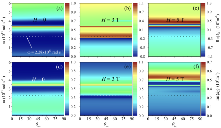
In Fig. 2 we show the real part of the permittivity tensor elements and for different values of the magnitude of the external magnetic field. As one can see in panels (b) and (c), as the external magnetic field increases, there appear broader frequency regions in which the real parts of and have opposite signs, which is the necessary condition for the hyperbolic modes to exist. In those regions, and as explained in the previous section, the uniaxial approximation predicts that incoming waves may be refracted into the slab as hyperbolic waves with given by the expression of Eq. (7).
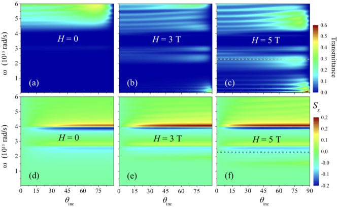
Now we turn to the analysis of the refraction of a plane wave impinging in our InSb slab. In particular, we focus on the case of TM-polarized plane waves since, as we discussed in the previous section, these are the ones that can undergo anomalous refraction. The required calculations for the analysis of this phenomenon are relatively straightforward and can be carried out with standard methods of multilayer systems made of optically anisotropic materials Yeh1988 . In our case, we have made use of the scattering-matrix method of Ref. Caballero2012 . Let us emphasize that from now on, unless stated otherwise, we present numerically exact results obtained using the full structure of the permittivity tensor, including the off-diagonal elements and the real and imaginary parts of the different elements, as described in Eq. (8). In Fig. 3(a-c) we show the transmittance through a 50 m-thick InSb slab as a function of the frequency and the angle of incidence for a TM-polarized plane wave and several values of the magnetic field. Notice that the field changes significantly the transmittance through the slab in several frequency regions.
In order to determine whether the anomalous refraction may take place in this system, we also show in Fig. 3(d-f) the -component of the Poynting vector for the same cases as in panels (a-c). Let us stress that in this figure we evaluate the Poynting vector inside the slab right at the interface in which the plane wave impinges. As one can see, the -component of the Poynting vector is actually negative for some frequencies and when this occurs, it remains negative for any angle of incidence. It is important to stress that these frequency regions are in all cases regions where the real parts of and have opposite signs, i.e., they correspond to regions where the hyperbolic modes exist (at least in the uniaxial approximation). These results demonstrates that indeed a slab of a doped semiconductor can exhibit a magnetic-field induced and controlled anomalous refraction.
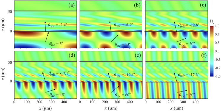
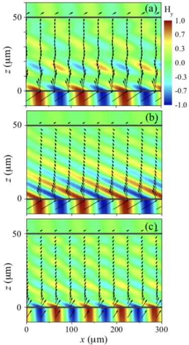
In order to get a deeper insight into how this anomalous refraction takes place, we now analyze in more detail its angle dependence. For this purpose, we present in Fig. 4 results for spatial distribution of the -component of the magnetic field when a TM-polarized plane wave impinges on a 50 m-thick slab at different angles of incidence. In this case, we have fixed the magnitude of the external field to 5 T and we have chosen a frequency of rad/s. With these parameters, the hyperbolic condition is fulfilled, i.e., the real parts of and have opposite signs, see Fig. 2 and also Fig. 3(c,f). In the different panels of Fig. 4 we provide the result for the angle that indicates the direction of the Poynting vector immediately after the wave crosses the first interface. Notice that irrespective of the angle of incidence, the angle is always negative, which indicates that an anomalous refraction takes place. This fact confirms, in turn, the predictions made in the previous section based on the uniaxial approximation, namely the fact that an external magnetic field may cause the anomalous refraction of an incident wave immediately after it enters into the slab, as well as the absence of a critical angle.
As we have pointed out several times already, a doped semiconductor under an external magnetic field is not exactly equivalent to a hyperbolic material. The external magnetic field also induces off-diagonal elements of the permittivity tensor that are responsible for the polarization conversion and the corresponding magneto-optical effects. Moreover, these elements modify the dispersion relation of the propagating waves inside the slab, as we briefly discuss in Appendix A. In this sense, one may wonder what their role is in this anomalous refraction. To answer this question, we present in Fig. 5(a,b) a comparison of the results for the spatial distribution of the Poynting vector in a case where the anomalous refraction takes place, which were computed taking into account the full structure of the permittivity tensor (), panel (a), and with the uniaxial approximation (), panel (b). The different parameters are indicated in the caption of that figure.
For the sake of comparison, we show in Fig. 5(c) the exact results for the Poynting vector in the case of a frequency where there are no hyperbolic modes. As one can see in Fig. 5(a) for the exact results, the -component of the Poynting vector inside the slab oscillates between negative (anomalous refraction) and positive (conventional refraction) values, which is due to the polarization conversion that occurs inside the slab due to the magneto-optical activity. This is in marked contrast with the results shown in Fig. 5(b) that were computed with the uniaxial approximation and therefore, there is no polarization conversion. In this case, the anomalous refraction survives throughout the slab, with the magnitude of the Poynting vector decaying inside the slab simply due to the absorption in this material. These results illustrate the basic difference in the anomalous refraction between semiconductors under a magnetic field and ideal hyperbolic materials. Let us say to conclude this section that Fig. 5(c) illustrates the fact that in the more conventional case when the real parts of and have the same sign, then the -component of the Pointing vector only takes positive values, irrespective of the fact that there is some degree of polarization conversion due to the fact that .
IV Partial focusing
The occurrence of anomalous refraction in doped semiconductors under a static magnetic field naturally raises the question of whether other related phenomena can also take place in these systems. For instance, it is well-known that the anomalous refraction in hyperbolic metamaterials enables the realization of lenses analogue to the superlens made from negative-index metamaterials Poddubny2013 . A basic difference, however, is the fact that while in negative-index materials the group and phase velocities are always antiparallel, in the case of hyperbolic metamaterials the relative orientation of those two velocities depends on the propagation direction relative to the principal axis. This fact results in partial focusing of radiation by a hyperbolic metamaterial slab Smith2003 ; Fang2009 ; Liu2009 ; Li2011 , a phenomenon that has been observed for microwaves Smith2004 . In this respect, the goal of this section is to explore the possibility of observing partial focusing in slabs made of doped semiconductors under an external magnetic field.
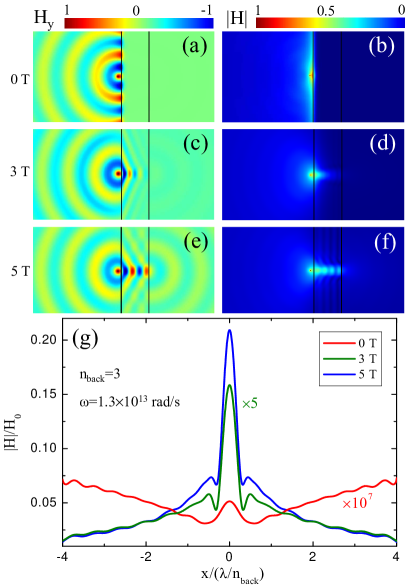
For this purpose, we have carried out a series of finite-element simulations exploring the occurrence of focusing phenomena in the 50 m thick doped InSb slabs studied in the previous section under plane wave illumination. The calculations were performed using the frequency-domain Maxwell’s Equation solver implemented in COMSOL MULTIPHYSICSTM, the frequency of operation was set to rad/s, and the tunability of the response of the system against the external static magnetic field was analyzed. The external excitation was a point-like magnetic field source of the form , located m away from the doped InSb surface. In order to reduce the impedance mismatch, enhance transmission, and improve the visibility of the magnetic fields, we set the background refractive index to , which is a good approximation for bulk semiconductors such as GaN or ZnS in the far-infrared range Han2007 .
Figure 6 shows the -component (left panels) and magnitude (right panels) of the magnetic fields for three different amplitudes of the static field : 0 T (a-b), 3 T (c-d) and 5 T (e-f). The amplitude in all field maps are normalized to 1. We can observe that in the absence of static fields, the slab is completely opaque, as expected from Fig. 2(a), and it behaves as a perfect conductor (with very large, negative and isotropic permittivity). Applying an external magnetostatic field, the transmission increases, see Fig. 3, as the permittivity becomes hyperbolic. At 3 and 5 T, the transmitted fields concentrate at the output, in the near-field of the slab, the signature of the focusing effect we were seeking for. Figure 6(g) displays the amplitude of the transmitted magnetic field normalized to evaluated at the surface of the slab, showing that despite the absence of curvature in the slab, it indeed acts as a lens, able to yield high-resolution images of the excitation source. We note that the plots in Fig. 6 were obtained through 2D calculations assuming translational symmetry in the fields along -direction. The off-diagonal terms in the permittivity were not accounted for in these simulations. In order to test their impact in the partially-focused field profiles, we also performed more coarsely meshed full 3D calculations and they are discussed in Appendix A. Those results allowed us to conclude that a non-vanishing only reduce the transmissivity of the slab, without diminishing its lensing performance.
V Conclusions
In summary, we have demonstrated in this work that the application of an external magnetic field may induce anomalous refraction at the interface between a dielectric media and a doped semiconductor. We have illustrated this phenomenon with the example of InSb, a polar semiconductor, but we anticipate that this phenomenon can take place in a great variety of semiconductors, including non-polar ones such as Si. The anomalous refraction and focusing effect reported in this work occurs in the infrared region of the electromagnetic spectra and it is not restricted by the angle of incidence. We have also discussed the similarities with the anomalous refraction that takes place in hyperbolic metamaterials and the differences due to the magneto-optical activity of semiconductors under a static magnetic field. Moreover, we have shown that the occurrence of this anomalous refraction enables planar semiconductor slabs to partially focus the electromagnetic radiation. A salient feature of the phenomenona predicted in this work is that, contrary to what happens in hyperbolic metamaterials, they only require naturally occurring materials and they can be tuned at will with an external field. We think that our work can trigger off the realization of experiments aiming at the confirmation of our predictions and it can also stimulate theoretical work investigating related physical phenomena such as subwavelength imaging or magnetic-field controlled wave-guiding.
Acknowledgments
We thank A. García-Martín for fruitful discussions. E.M.-V. was financially supported by the Dirección de Investigaciones of the Universidad Pedagógica y Tecnológica de Colombia. A.I.F.-D. acknowledges funding from the Spanish Ministry of Economy and Competitiveness (MINECO, contract No. FIS2015-64951-R) and the EU Seventh Framework Programme under Grant Agreement FP7-PEOPLE-2013-CIG-630996. J.C.C. thanks MINECO (contract No. FIS2017-84057-P) for financial support as well as the DFG and SFB 767 for sponsoring his stay at the University of Konstanz as Mercator Fellow.
Appendix A Additional results
We present in this appendix additional results to clarify and back up some of the statements made in the main body of the paper. First of all, and for the sake of completeness, we present here the exact dispersion relation of the propagating modes in the InSb slab under a magnetic field. Taking into account the full structure of the permittivity tensor in Eq. (2), we obtain the following dispersion relation for TE waves (propagating in the plane)
| (9) |
while for the TM waves this relation adopts the form
| (10) |
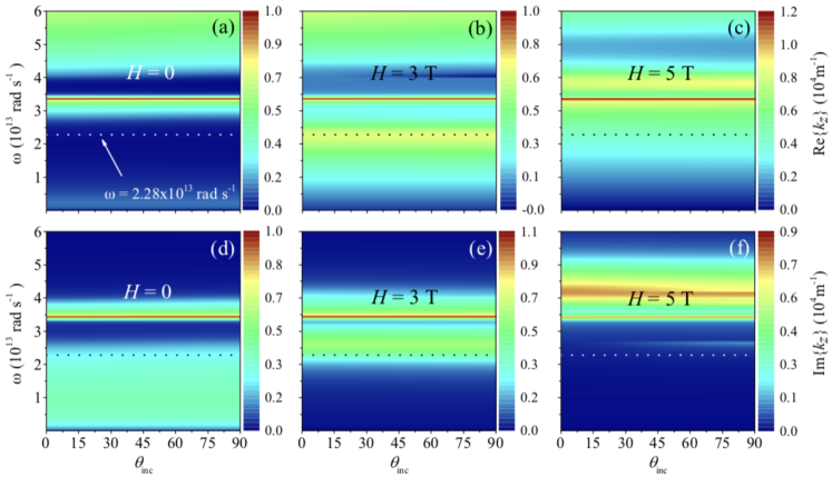
where . These relations are rather involved. For this reason, and in order to evaluate the impact of the off-diagonal elements of the permittivity tensor, we have plotted these full relations in Fig. 7 for different values of the magnetic field. In particular, we show both the real and the imaginary part of as a function of the frequency and the angle of incidence. To compare with the uniaxial approximation discussed in section II, we show in Fig. 8 the corresponding results for the dispersion relation assuming that the off-diagonal elements vanish. As one can see, there are no dramatic differences, which explains in particular why the uniaxial approximation is able to describe the conditions at which the anomalous refraction occurs.
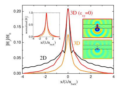
Finally, in Fig. 9 we present the results corresponding to Fig. 6 for the focusing with an external field of 5 T, but this time computed with a full 3D simulation that takes into account the off-diagonal elements of the permittivity tensor. For comparison, we also include in this figure the results obtained with a 3D simulation without magneto-optics () and those of the 2D simulation of Fig. 6. Mimicking the 2D configuration, the source in the 3D calculations is a line dipole along the -direction. The convergence of results against the truncation of the simulation volume along this direction has been checked. As one can see, a significant focusing survives in the full 3D simulations and the main characteristics of the field distribution are indeed very similar to those reported in Fig. 6 with the 2D approximation.
References
- (1) V. G. Veselago, Sov. Phys. Usp. 10, 509 (1968).
- (2) V. M. Shalaev, Nat. Photon. 1, 41 (2007).
- (3) J. B. Pendry and D. Smith, Physics Today 57, 6 (2004).
- (4) J. Han, A. Lakhtakia, and C.-W. Qiu, Opt. Express 16, 19 (2008).
- (5) A. Poddubny, I. Iorsh, P. Belov, and Y. Kivshar, Nat. Photon. 7, 948 (2013).
- (6) L. Ferrari, C. Wu, D. Lepage, X. Zhang, Z. Liu, Progress in Quantum Electronics 40, 1 (2015).
- (7) L. Hu and S. T. Chui, Phys. Rev. B 66, 085108 (2002).
- (8) E. Moncada-Villa, V. Fernández-Hurtado, F. J. García-Vidal, A. García-Vidal, and J. C. Cuevas, Phys. Rev. B 92, 125418 (2015).
- (9) E. D. Palik, R. Kaplan, R. W. Gammon, H. Kaplan, R. F. Wallis, and J. J. Quinn, Phys. Rev. B 13, 2497 (1976).
- (10) P. Ben-Abdallah, Phys. Rev. Lett. 116, 084301 (2016).
- (11) L. Zhu and S. Fan, Phys. Rev. Lett. 117, 134303 (2016).
- (12) R. M. Abraham Ekeroth, P. Ben-Abdallah, J. C. Cuevas, A. García-Martín, ACS Photonics 5, 705 (2018).
- (13) B. H. Cheng, H. W. Chen, K. J. Chang, Y.-C. Lan, and D. P. Tsai, Scientific Reports 5, 18172 (2015).
- (14) K. V. Sreekanth, Y. Alapan, M. ElKabbash, E. Ilker, M. Hinczewski, U. A. Gurkan, A. De Luca, and G. Strangi, Nat. Mat. 15, 621 (2016).
- (15) H. J. Lezec, J. A. Dionne, and H. A. Atwater, Science 316, 430 (2007).
- (16) A. Zvezdin and V. Kotov, Modern Magnetooptics and Magnetooptical Materials (IOP, Bristol, 1997).
- (17) P. Yeh, Optical Waves in Layered Media (Wiley, New York, 1988).
- (18) B. Caballero, A. García-Martín, and J. C. Cuevas, Phys. Rev. B 85, 245103 (2012).
- (19) D. R. Smith and D. Schurig, Phys. Rev. Lett. 90, 077405 (2003).
- (20) A. Fang, T. Koschny, and C. M. Soukoulis, Phys. Rev. B 79, 245127 (2009).
- (21) H. Liu, Q. Lv, H. Luo, S. Wen, W. Shu, and D. Fan, J. Opt. A 11, 105103 (2009).
- (22) G. Li, J. Li, K. W. Cheah, Appl. Opt. 50, G27 (2011).
- (23) D. R. Smith, D. Schurig, J. J. Mock, P. Kolinko, and P. Rye, Appl. Phys. Lett. 84, 2244 (2004).
- (24) J. Han, A. K. Azad, and W. Zhan, Nanoelectron. Optoelectron. 2, 222 (2007).