MOVPE growth of N-polar AlN on 4H-SiC: effect of substrate miscut on layer quality
Abstract
We present the effect of miscut angle of SiC substrates on N-polar AlN growth. The N-polar AlN layers were grown on C-face 4H-SiC substrates with a miscut towards by metal-organic vapor phase epitaxy (MOVPE). The optimal V/III ratios for high-quality AlN growth on 1∘ and 4∘ miscut substrates were found to be 20000 and 1000, respectively. MOVPE grown N-polar AlN layer without hexagonal hillocks or step bunching was achieved using a 4H-SiC substrate with an intentional miscut of 1∘ towards . The 200-nm-thick AlN layer exhibited X-ray rocking curve full width half maximums of 203 arcsec and 389 arcsec for (002) and (102) reflections, respectively. The root mean square roughness was 0.43 nm for a 2 atomic force microscope scan.
keywords:
A1. Polarity, A1. X-ray diffraction, A3. Metal-organic vapor phase epitaxy, B1. Nitrides, B2. Semiconducting aluminum compounds1 Introduction
III-nitride (III-N) semiconductors have received much attention for optical and electrical applications. AlN holds much promise for high-temperature and high-power applications due to its high critical electric field, wide band-gap energy and high thermal conductivity [1, 2]. An AlN-channel field-effect transistor has been demonstrated recently [2]. However, there are challenges in the charge carrier mobility and contact resistances. These limitations could be overcome by employing nitrogen-polar AlN-based heterostructures.
Wurtzite structure of III-Ns has two types of polar planes, metal-polar (001) and nitrogen-polar (00). Generally, III-N high-electron mobility transistors (HEMTs) employ a metal polar AlGaN/GaN structure, which has many merits in crystal growth, i.e., smooth surface, high crystalline quality and low impurity concentrations. However, the performance of metal-polar HEMTs is limited by high contact resistances to the top AlGaN layer and by large leakage current through the GaN buffer layer. In contrast N-polar HEMTs have a reversed structure of GaN/AlGaN layers. The top GaN layer offers low contact resistances [3]. The AlGaN buffer layers with higher band-gap act as a natural back barrier and provide a low leakage current. For N-polar III-Ns HEMTs, high-Al content AlGaN buffer layers can reduce leakage current and induce high carrier concentrations. Thus, N-polar high-Al content AlGaN and AlN growth would be required for further high performance of III-Ns HEMTs.
N-polar AlN buffer layers would be the ideal transistor platform. However, the difficulties of N-polar III-Ns growth are limiting the performance of N-polar III-Ns HEMTs. N-polar III-Ns growth suffers from a high density of threading dislocations and large surface roughness compared to metal polar III-Ns [4, 5, 6, 7, 8, 9, 10, 11, 12].
In N-polar III-Ns growth, adatoms have a small diffusion length on surfaces due to high binding energy, limiting adatom transport to kink and step sites and promoting island formation on surface [13, 14]. N-polar III-Ns hetero-epitaxial growth has multi-micron hexagonal hillocks formed by inversion domains [15]. The inversion domains are attributed to the oxidation of substrate or the accumulation of group III atoms at low V/III ratios [7, 10]. Both surface islands and inversion domains increase surface roughness, making device fabrication unfeasible.
In metalorganic vapor phase epitaxy (MOVPE) growth of N-polar III-Ns, island formations are suppressed using an intentional miscut substrate because the high density of steps in high off-angle substrates enhance a step-flow growth mode [11, 16, 5]. However, the growth on high off-angle substrates causes step bunching phenomena, leading to macro steps [5, 11]. The step height increases with increasing layer thickness. The direct deposition of high-temperature (Al)GaN layers on an AlN nucleation layer causes macro-steps on the layer surface [17]. In contrast, step bunching in N-polar (Al)GaN growth is mitigated by nucleating a lower temperature (Al)GaN layer on a thin AlN nucleation layer [17, 18]. N-polar III-N devices using low-temperature nucleation layers have been demonstrated [19, 18]. These reports control the growth temperature of N-polar III-Ns at a fixed off angle of substrates. In N-polar AlN growth, there is room to improve the growth mode and crystalline quality by changing the off angle of substrates.
In a previous study, we have shown that the formation of hexagonal hillocks can be suppressed in N-polar AlN growth by using a low growth rate of 0.1 together with an increased temperature of 1150 [20]. In this paper we study the effect of miscut angle of C-face 4H-SiC substrate on MOVPE growth of N-polar AlN under various growth conditions.
2 Experiment
200-nm-thick N-polar AlN layers were grown on C-face of 4H-SiC substrates by MOVPE. The substrates had an intentional miscut of either 4∘ or 1∘ towards (M-plane). The SiC surfaces were cleaned in-situ for 20 min at nominal substrate surface temperature of 1180 in hydrogen () ambient at 150 mbar pressure prior to AlN growth. The substrate temperature was monitored using an emissivity corrected in-situ pyrometer. All temperature values in this work refer to pyrometer estimated substrate temperature. The MOVPE reactor had a close coupled showerhead configuration. The gap between the showerhead and the susceptor was 11 mm, the default value for this reactor. Trimethylaluminium (TMAl) and ammonia () were used as precursors for aluminum and nitrogen, respectively. AlN was grown at 1150 in pressure of 50 mbar with carrier gas. The reactor was cleaned between growth runs using high temperature and baking steps.
Three-axis high resolution X-ray diffraction (HR-XRD) measurements were performed to assess the crystalline quality of the AlN layers. Rocking curves around symmetrical (002) and skew-symmetrical (102) reflections were recorded. Full width half maximums (FWHMs) for the diffraction peaks were calculated using least-squares fitting of a Lorentzian line-shape. The setup consisted of an X-ray mirror, a 4 Ge (220) monochromator and an analyzer crystal. X-ray wavelength of copper emission line was used. Scanning electron microscope (SEM) images were observed in order to assess micrometer-sized surface structures, especially hexagonal hillocks. The surface roughness of the AlN layers was determined by atomic force microscopy (AFM).
3 Results and discussion
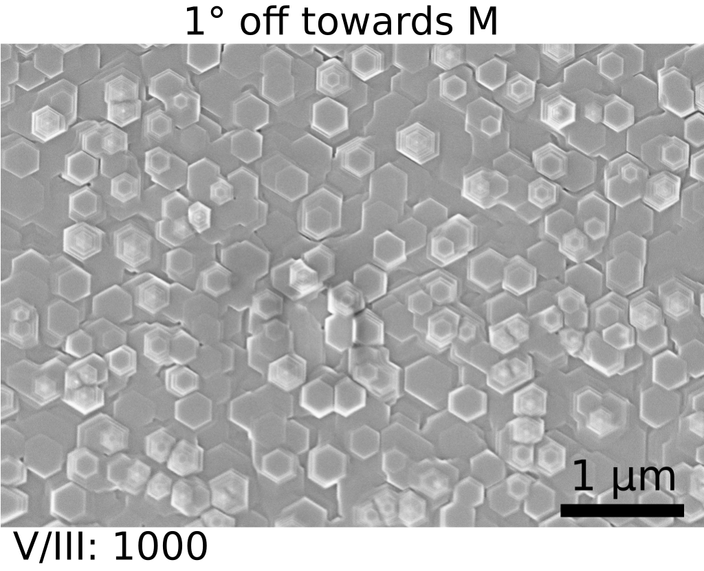
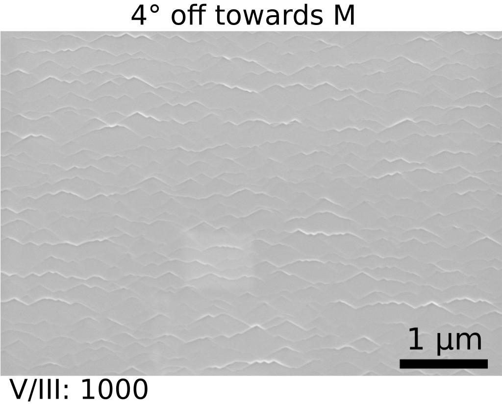
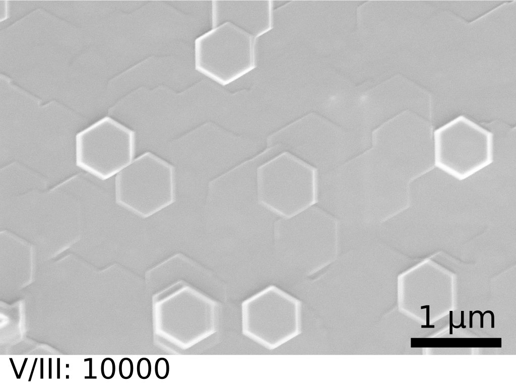
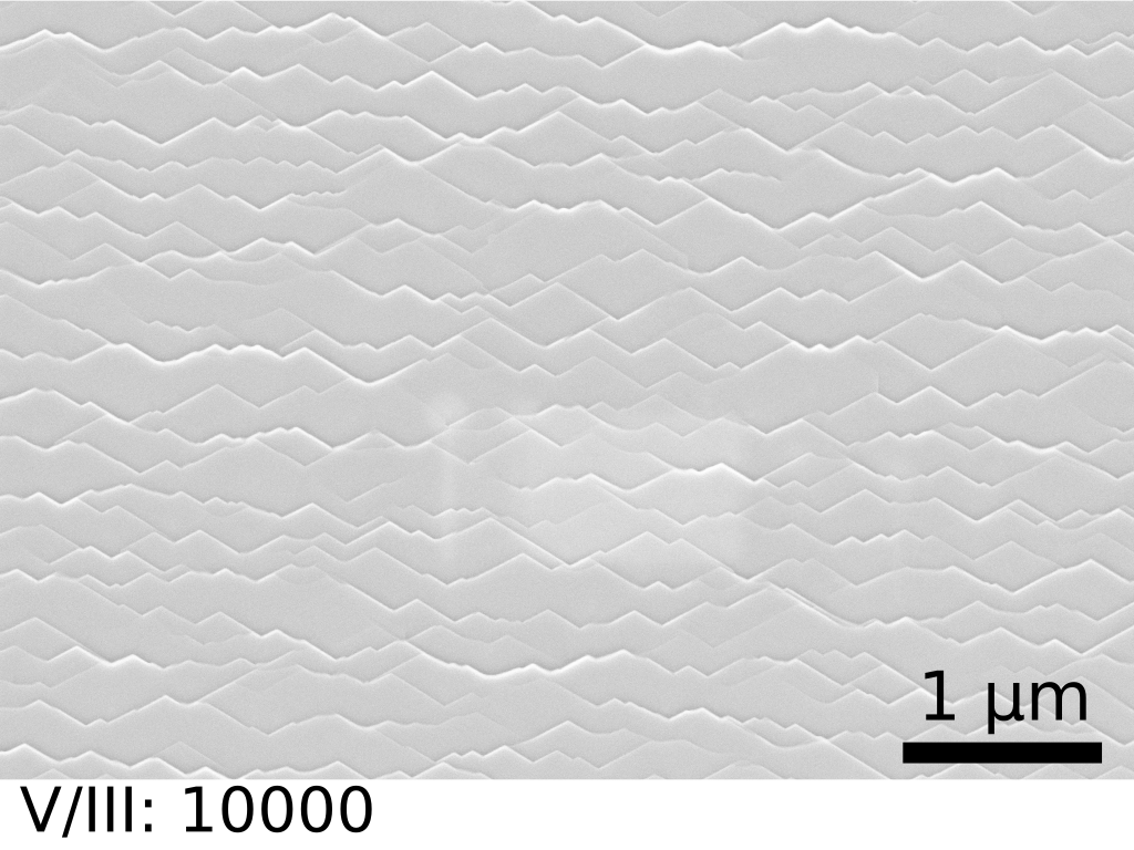
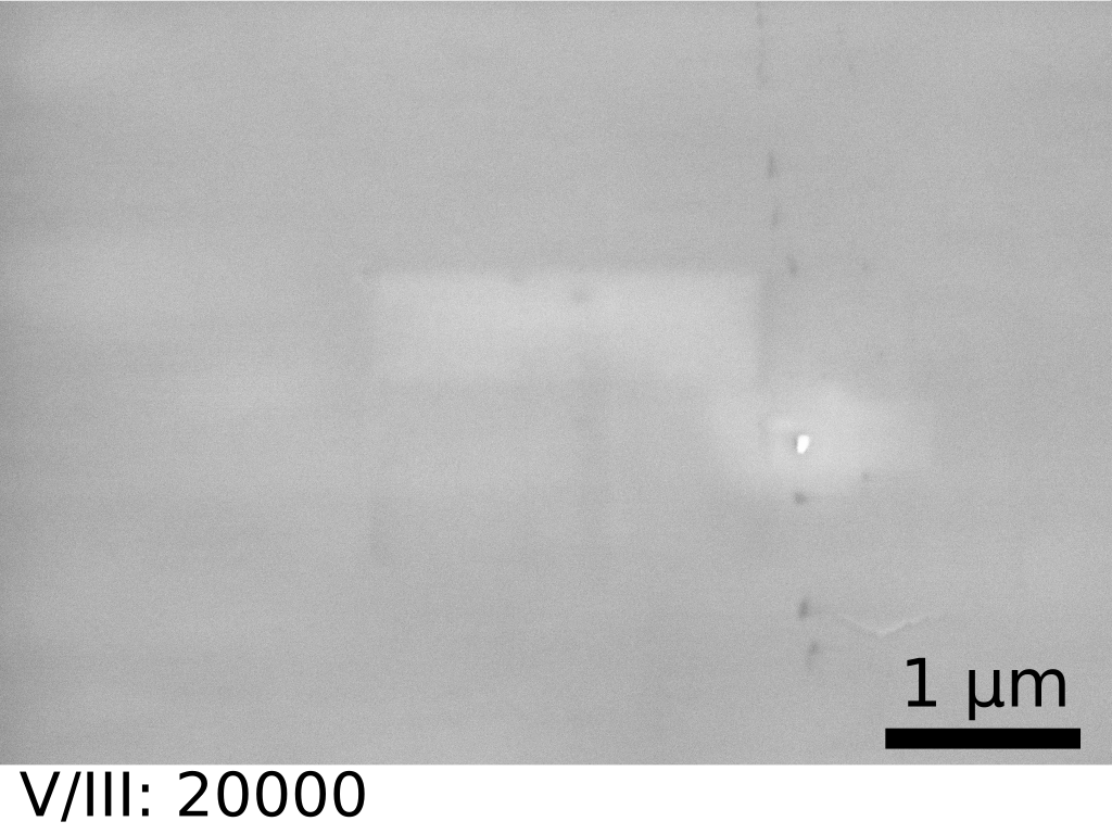
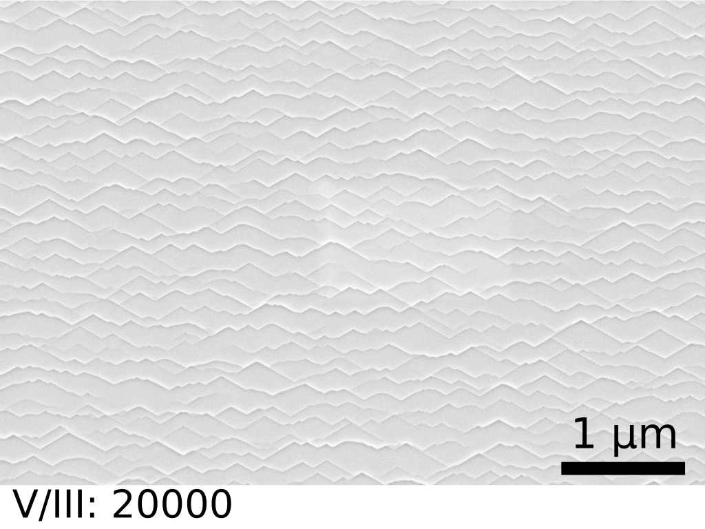
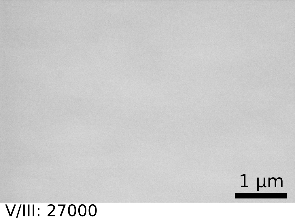
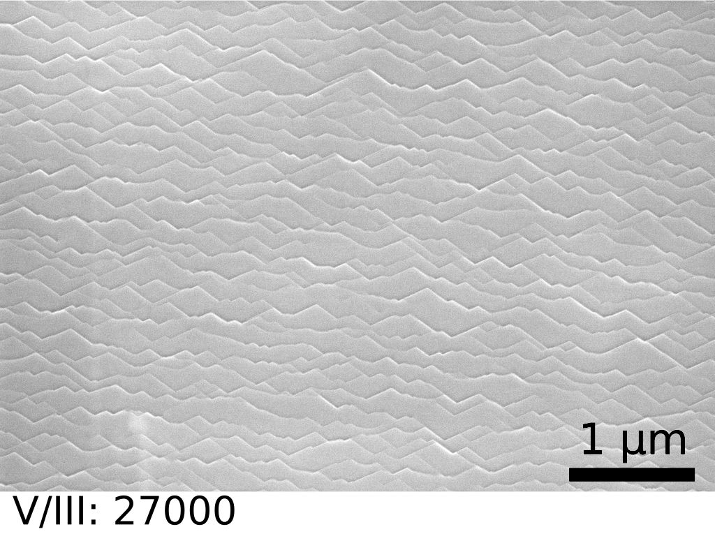
Figure 1 shows SEM images of N-polar AlN layers with 200 nm thickness. A series over a wide V/III range from 1000 to 27000 was grown to investigate the effect on N-polar growth in conjugation with the substrate miscut. The growth rate was maintained at 0.1 throughout the series by altering the precursor mass flows to limit the effect of the growth rate on crystalline quality. No multi-micrometer hexagonal hillocks caused by inversion domains were observed in these layers [15, 7]. All AlN layers grown on the 4∘ miscut substrate exhibited a step flow growth mode. We consider that the step bunching is caused by anisotropy in the terrace step adatom capture probabilities [21]. The anisotropy in capture probability leads to differences in step lateral advancement rates and can cause step-bunching. The surface roughness increases with increasing layer thickness, indicating that the step bunching effect is not self limiting [10].
V/III-ratio has a profound effect on surface morphology of the AlN layers grown on the 1∘ miscut subsrate. Inversion domains have been suggested to form on oxidized regions of the substrate or accumulation of Al-atoms at low V/III ratios [7, 10]. The AlN layer grown using the V/III-ratio of 1000 exhibits a high density of sub-micrometer hexagonal hillocks. We suggest that the sub-micrometer hillocks result from the enhancement of island formation on the surface terraces since no hillocks are observed on 4∘ miscut subsrates. The dependence of surface kinetics on vapor supersaturation has been used to explain the surface morphology of Al-polar AlN [22]. Decreasing the substrate miscut increases surface supersaturation, and thus, can promote island formation on the surface terraces if critical supersaturation is reached [22].
Increasing the V/III-ratio to 10000 significantly reduces the density of hexagonal hillocks and increases the hillock size. The high V/III ratio decreases the surface migration of Al-adatoms, promoting the incorporation of adatoms into the surface kink sites and reducing island formation probability on the surface terraces [11, 5, 23]. Increasing the V/III-ratio to 20000 suppresses the formation of hexagonal hillocks entirely. Further increase of V/III-ratio to 27000 produces an identical surface morphology. Increasing the V/III-ratio in this growth window shows the elimination of hillocks and the onset of step-flow growth which could suggest decreasing surface supersaturation. An alternative explanation could be offered based on the Al-adatom migration length. If critical supersaturation for island formation is reached on the surface terraces, the decreased migration length reduces the island capture and thus growth rate, analogous to step-bunching. However, it is difficult to estimate the dependence surface supersaturation on V/III-ratio due to various process parameters. Further investigation on the relation between V/III-ratio and supersaturation is necessary.
In comparison with the 4∘ miscut substrates, no step bunching is observed in a micron scale for the AlN layers grown on 1∘ miscut substrate. The behavior could be attributed to wider surface terraces due to the decreased miscut. Decreasing the miscut angle has been shown to increase the parameter window for step-flow growth as the change between the dominating growth mode is less abrupt [21]. If the diffusion length of the ad-atoms is greater than the surface terrace width, step bunching morphology becomes more probable. Al diffusion length of 31 nm has been estimated for Al-polar AlN while N-polar AlN exhibits a shorter diffusion lenght [24, 14]. By assuming that the two-bilayer-high steps formed on the SiC surfaces during the surface cleaning are uniformly distributed, the average terrace width is 28.9 nm and 7.24 nm for 1∘ and 4∘ miscut 4H-SiC substrate, respectively [25, 26].
Figure 2 presents X-ray rocking curves (XRC) around symmetrical (002) and skew-symmetrical (102) reflections for the V/III-ratio series. In III-Ns, screw dislocations contribute to the broadening of the (002) peak, while both screw and edge dislocations contribute to the broadening of the (102) peak [27]. Based on Figure 2, the crystalline quality of the N-polar AlN layers strongly depends on the V/III-ratio. The AlN layers grown on the 4∘ and 1∘ miscut substrates had vastly different optimum V/III-ratios which were 1000 and 20000, respectively. The smallest FWHMs were measured from the AlN layer grown on 4∘ miscut substrates with V/III ratio of 1000 were 232 arcsec and 514 arcsec for the (002) and the (102) scan, respectively. The FWHMs increase with increasing the V/III ratio, suggesting degrading crystalline quality. Based on our previous study we believe this to be the optimum V/III ratio since hexagonal hillocks were formed when V/III ratio was decreased below 1000 [20]. We consider that the step flow growth mode contributes to high crystalline quality.
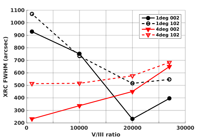
On the other hand, for the AlN layers grown on the 1∘ miscut substrates the V/III-ratio of 20000 resulted in the smallest FWHMs of the (002) and the (102) scans which were 231 arcsec and 515 arcsec, respectively. The higher V/III ratios than 20000 resulted in larger FWHMs, suggesting degrading crystalline quality. Somewhat analogous to the 4∘ miscut substrate, highest crystalline quality is achieved at the lowest V/III-ratio sufficient to suppress the formation of the hexagonal hillocks.
The highest reported crystalline quality in N-polar AlN has been achieved with molecular beam epitaxy. A 200-nm-thick N-polar AlN layer was coherently grown on SiC at very low growth temperature exhibiting XRC FWHMs of 120 arcsec and 210 arcsec for (002) and (102) scans [28]. On the other hand, relaxed AlN grown on SiC by MOVPE, an AlN layer grown using V/III-ratio of 24000 showed small XRC FWHMs of 468 arcsec and 684 arcsec for (002) and (102) scans, respectively [11]. Despite relaxation, we achieved further high crystalline quality in N-polar AlN MOVPE growth.
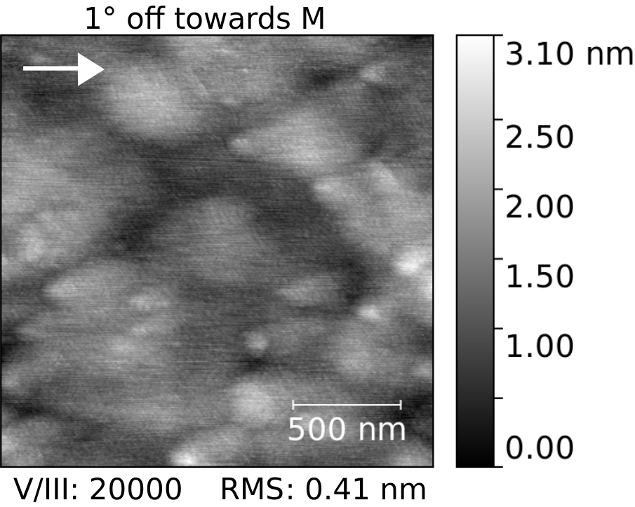
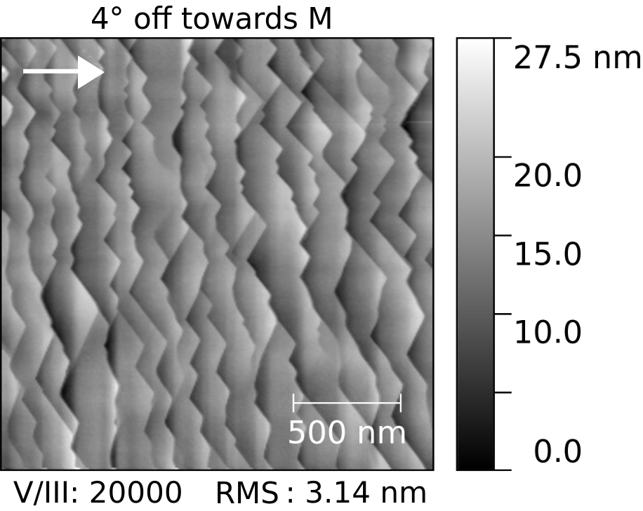
Figure 3 presents AFM images from the AlN layers grown on 1∘ (top) and 4∘ (bottom) miscut substrates with a V/III-ratio of 20000. The surface of the AlN layer grown on the 1∘ miscut subsrate is smooth with a root-mean-square (RMS) roughness of 0.41 nm. No step bunching or hexagonal hillocks are seen. In contrast, the AlN layer grown on the 4∘ miscut subsrate has a high RMS roughness of 3.14 nm due to step bunching, with an average step height of 9 nm. The steps propagate towards the substrate miscut of , indicating step-flow growth mode. This indicates that it is possible to achieve simultaneous suppression of hexagonal hillocks and step bunching for N-polar AlN by controlling the Al-adatom migration with optimal growth conditions on low off-axis substrates. When compared to previous results, AFM 2 scan RMS roughness of 1.1 nm and 2 nm have been reported for 90-nm and 120-nm-thick N-polar AlN grown on SiC, respectively [11, 10]. In these studies, the large roughness of N-polar AlN surfaces were attributed to step bunching. N-polar III-Ns grown on substrates with miscut angle lower than 2∘ by MOVPE exhibited a high density of hexagonal hillocks [5]. 160-nm-thick N-polar AlN on 0.2∘-off axis SiC grown by MBE exhibited 0.6 nm RMS roughness despite existence of hexagonal hillocks with a density of [28].
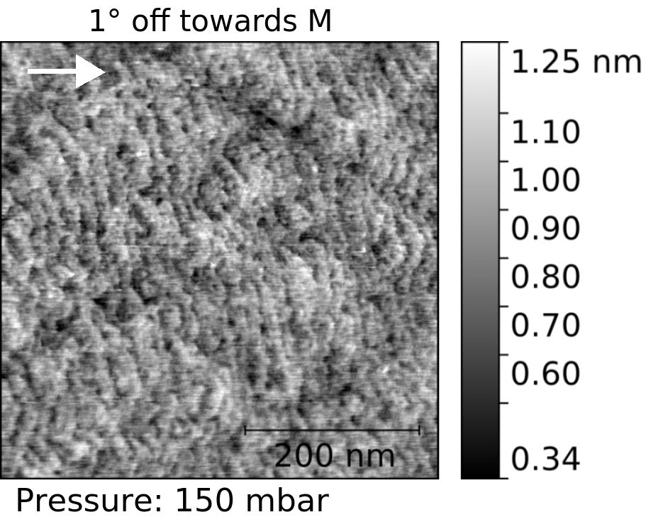
The substrate preparation prior to growth can have a significant impact on the crystalline quality of the epitaxial layer. The substrate surface cleaning used in the V/III-series was originally optimized for the 4∘ miscut substrate. A pressure of 100 mbar was then used during the substrate cleaning. Changing the cleaning conditions can effect the surface profile significantly [25, 26]. Figure 4 presents AFM images of 4H-SiC substrates after 20 min cleaning in atmosphere using 150 mbar pressure (top) and 100 mbar pressure (bottom) at 1180 nominal substrate surface temperature. It can be seen that two-bilayer-high steps have formed on the substrate surfaces. The average calculated terrace width was 20 nm and 18 nm for 150 mbar and 100 mbar cleaning pressures, respectively, roughly corresponding to the previously calculated estimate of 28.9 nm. The difference could be due to a slight variation between the nominal and actual miscut angle. Based on Figure 4 the 100 mbar cleaning pressure creates a well defined step-and-terrace structure whereas the substrate cleaned in 150 mbar pressure shows a more meandering step profile.
Using 100 mbar cleaning pressure, 200-nm-thick AlN layers were grown on 1∘ and 4∘ miscut substrates using a V/III-ratio of 20000. Figure 5 presents a large area SEM image of the AlN layer grown on the 1∘ miscut substrate. No hexagonal hillocks or other defects were discovered.
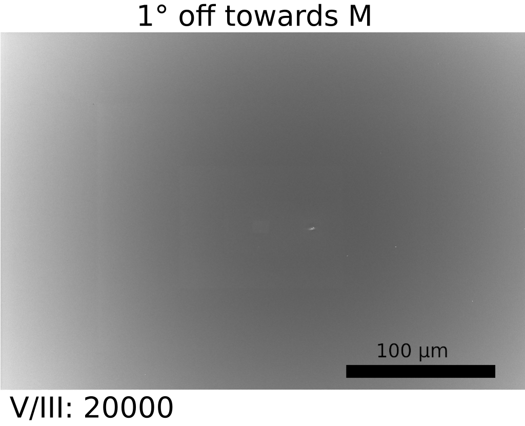
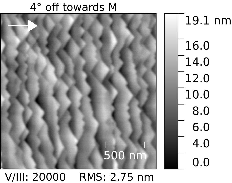
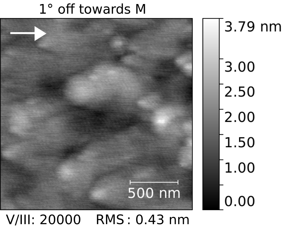
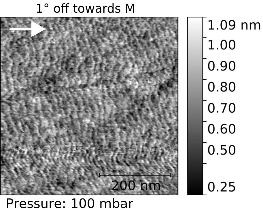
Figure 6 presents 2 AFM images from the AlN layers grown on 1∘ (top) and 4∘ (bottom) miscut substrates. Compared to the AlN layers in Figure 3, changing the substrate cleaning pressure has no significant effect on the layer morphology or RMS roughness. The RMS roughnesses were 0.43 nm and 2.75 nm for AlN layers grown on 1∘ and 4∘ miscut substrate, respectively. The crystalline quality of AlN layers grown on the 1∘ miscut substrates was improved. XRC FWHMs of 203 and 389 arcsec for (002) and (102) reflections were measured, from a sample grown on the 1∘ miscut substrate using the optimal V/III-ratio of 20000 together with substrate cleaning pressure of 100 mbar. We achieved the highest crystalline-quality N-polar AlN layers grown by MOVPE.
4 Conclusions
200-nm-thick N-polar AlN layers were grown by MOVPE on C-surface of SiC-4H substrates with an intentional miscut of 1∘ or 4∘ towards . The optimal V/III-ratios for 1∘ and 4∘ miscut substrates were found to be 20000 and 1000, respectively. MOVPE grown N-polar AlN layer without hexagonal hillocks or step bunching was achieved using a 4H-SiC substrate with an intentional miscut of 1∘. The XRC FWHMs were 203 arcsec and 389 arcsec for (002) and (102) reflections, respectively. The RMS surface roughness was 0.43 nm for AFM 2 scan. We found that the high V/III ratio and small off angle of substrates contributes to high crystalline quality in high-temperature N-polar AlN growth.
Acknowledgements
This work was supported by the Academy of Finland (grant 297916), the Foundation for Aalto University Science and Technology and JSPS KAKENHI Grant No. 16H06424 and 17K14110. The research was performed at the OtaNano - Micronova Nanofabrication Centre of Aalto University.
References
References
- [1] H. Morkoç, General properties of nitrides, Handbook of Nitride Semiconductors and Devices: Materials Properties, Physics and Growth 1 (2008) 1–129.
- [2] H. Okumura, S. Suihkonen, J. Lemettinen, A. Uedono, Y. Zhang, D. Piedra, T. Palacios, AlN metal-semiconductor field-effect transistors using Si-ion implantation, International Conference on Solid State Devices and Materials (N-2-06, 641).
-
[3]
M. H. Wong, S. Keller, N. Dasgupta, D. J. Denninghoff, S. Kolluri, D. F. Brown,
J. Lu, N. a. Fichtenbaum, E. Ahmadi, U. Singisetti, A. Chini, S. Rajan, S. P.
DenBaars, J. S. Speck, U. K. Mishra,
N-polar GaN
epitaxy and high electron mobility transistors, Semiconductor Science and
Technology 28 (7) (2013) 74009.
doi:10.1088/0268-1242/28/7/074009.
URL http://iopscience.iop.org/0268-1242/28/7/074009/article/ - [4] S. Keller, H. Li, M. Laurent, Y. Hu, N. Pfaff, J. Lu, D. F. Brown, N. a. Fichtenbaum, J. S. Speck, S. P. Denbaars, U. K. Mishra, Recent progress in metal-organic chemical vapor deposition of (000-1) N-polar group-III nitrides, Semiconductor Science and Technology 29 (2014) 113001. doi:10.1088/0268-1242/29/11/113001.
- [5] S. Keller, N. A. Fichtenbaum, F. Wu, D. Brown, A. Rosales, S. P. Denbaars, J. S. Speck, U. K. Mishra, Influence of the substrate misorientation on the properties of N-polar GaN films grown by metal organic chemical vapor deposition, Journal of Applied Physics 102 (8). doi:10.1063/1.2801406.
- [6] S. Keller, Y. Dora, F. Wu, X. Chen, S. Chowdury, S. P. Denbaars, J. S. Speck, U. K. Mishra, Properties of N-polar GaN films and AlGaN/GaN heterostructures grown on (111) silicon by metal organic chemical vapor deposition, Applied Physics Letters 97 (14) (2010) 1–4. doi:10.1063/1.3499428.
- [7] J. Weyher, P. Brown, A. Zauner, S. Müller, C. Boothroyd, D. Foord, P. Hageman, C. Humphreys, P. Larsen, I. Grzegory, S. Porowski, Morphological and structural characteristics of homoepitaxial GaN grown by metalorganic chemical vapour deposition (MOCVD), Journal of Crystal Growth 204 (4) (1999) 419–428. doi:10.1016/S0022-0248(99)00217-1.
- [8] T. Matsuoka, Y. Kobayashi, H. Takahata, T. Mitate, S. Mizuno, A. Sasaki, M. Yoshimoto, T. Ohnishi, M. Sumiya, N-polarity GaN on sapphire substrate grown by MOVPE, Physica Status Solidi (B) Basic Research 243 (7) (2006) 1446–1450. doi:10.1002/pssb.200565456.
- [9] S. Keller, C. S. Suh, Z. Chen, R. Chu, S. Rajan, N. A. Fichtenbaum, M. Furukawa, S. P. DenBaars, J. S. Speck, U. K. Mishra, Properties of N-polar AlGaN/GaN heterostructures and field effect transistors grown by metalorganic chemical vapor deposition, Journal of Applied Physics 103 (3) (2008) 1–5. doi:10.1063/1.2838214.
- [10] S. Keller, N. Fichtenbaum, F. Wu, G. Lee, S. P. Denbaars, J. S. Speck, U. K. Mishra, Effect of the nucleation conditions on the polarity of AlN and GaN films grown on C-face 6H-SiC, Japanese Journal of Applied Physics, Part 2: Letters 45 (8-11). doi:10.1143/JJAP.45.L322.
-
[11]
D. Won, J. M. Redwing,
Effect of AlN buffer
layers on the surface morphology and structural properties of N-polar GaN
films grown on vicinal C-face SiC substrates, Journal of Crystal Growth 377
(2013) 51–58.
doi:10.1016/j.jcrysgro.2013.04.038.
URL http://dx.doi.org/10.1016/j.jcrysgro.2013.04.038 - [12] D. Won, X. Weng, Z. Y. Al Balushi, J. M. Redwing, Influence of growth stress on the surface morphology of N-polar GaN films grown on vicinal C-face SiC substrates, Applied Physics Letters 103 (24). doi:10.1063/1.4845575.
-
[13]
T. K. Zywietz, J. Neugebauer, M. Scheffler,
The
adsorption of oxygen at GaN surfaces, Applied Physics Letters 74 (12)
(1999) 1695.
doi:10.1063/1.123658.
URL http://scitation.aip.org/content/aip/journal/apl/74/12/10.1063/1.123658 - [14] T. Zywietz, J. Neugebauer, M. Scheffler, Adatom diffusion at GaN (0001) and (0001̄) surfaces, Applied Physics Letters 73 (4) (1998) 487–489. arXiv:9809006, doi:10.1063/1.121909.
- [15] A. R. A. Zauner, E. Aret, W. J. P. Van Enckevort, J. L. Weyher, S. Porowski, J. J. Schermer, Homo-epitaxial growth on the N-face of GaN single crystals: The influence of the misorientation on the surface morphology, Journal of Crystal Growth 240 (1-2) (2002) 14–21. doi:10.1016/S0022-0248(01)02389-2.
- [16] A. R. A. Zauner, J. L. Weyher, M. Plomp, V. Kirilyuk, I. Grzegory, W. J. P. Van Enckevort, J. J. Schermer, P. R. Hageman, P. K. Larsen, Homo-epitaxial GaN growth on exact and misoriented single crystals: suppression of hillock formation, Journal of Crystal Growth 210 (4) (2000) 435–443. doi:10.1016/S0022-0248(99)00886-6.
- [17] D. F. Brown, S. Keller, F. Wu, J. S. Speck, S. P. DenBaars, U. K. Mishra, Growth and characterization of N-polar GaN films on SiC by metal organic chemical vapor deposition, Journal of Applied Physics 104 (2) (2008) 1–6. doi:10.1063/1.2956329.
- [18] S. Kolluri, S. Member, S. Keller, S. P. Denbaars, U. K. Mishra, Microwave Power Performance N-Polar GaN MISHEMTs Grown by MOCVD on SiC Substrates Using an Al2O3 Etch-Stop Technology, IEEE Electron Device Letters 33 (1) (2012) 44–46.
- [19] D. F. Brown, R. Chu, S. Keller, S. P. Denbaars, U. K. Mishra, Electrical properties of N-polar AlGaN/GaN high electron mobility transistors grown on SiC by metalorganic chemical vapor deposition, Applied Physics Letters 94 (15) (2009) 148–151. doi:10.1063/1.3122347.
- [20] J. Lemettinen, H. Okumura, I. Kim, M. Rudzinski, J. Grzonka, T. Palacios, S. Suihkonen, Movpe growth of nitrogen- and aluminum-polar aln on 4h-sic, Journal of Crystal Growth.
- [21] K. Bellmann, U. W. Pohl, C. Kuhn, T. Wernicke, M. Kneissl, Controlling the morphology transition between step-flow growth and step-bunching growth, Journal of Crystal Growth 478 (2017) 187–192.
- [22] I. Bryan, Z. Bryan, S. Mita, A. Rice, J. Tweedie, R. Collazo, Z. Sitar, Surface kinetics in aln growth: A universal model for the control of surface morphology in iii-nitrides, Journal of Crystal Growth 438 (2016) 81–89.
- [23] S. Kim, J. Oh, J. Kang, D. Kim, J. Won, J. W. Kim, H. K. Cho, Two-step growth of high quality GaN using V/III ratio variation in the initial growth stage, Journal of Crystal Growth 262 (1-4) (2004) 7–13. doi:10.1016/j.jcrysgro.2003.10.009.
- [24] R. G. Banal, M. Funato, Y. Kawakami, Surface diffusion during metalorganic vapor phase epitaxy of AlN, Physica Status Solidi C 6 (2) (2009) 599 – 602. doi:10.1002/pssc.200880415.
- [25] S. Soubatch, S. E. Saddow, S. P. Rao, W. Lee, M. Konuma, U. Starke, Structure and Morphology of 4H-SiC Wafer Surfaces after H¡sub¿2¡/sub¿-Etching, Materials Science Forum 483-485 (Cvd) (2005) 761–764. doi:10.4028/www.scientific.net/MSF.483-485.761.
- [26] K. Akiyama, Y. Ishii, S. Abe, H. Murakami, Y. Kumagai, H. Okumura, T. Kimoto, J. Suda, A. Koukitu, In situ gravimetric monitoring of thermal decomposition and hydrogen etching rates of 6H-SiC(0001) Si face, Japanese Journal of Applied Physics 48 (9 Part 1) (2009) 0955051–0955054. doi:10.1143/JJAP.48.095505.
- [27] M. Moram, M. Vickers, X-ray diffraction of III-nitrides, Reports on Progress in Physics 72 (3) (2009) 036502.
- [28] H. Okumura, T. Kimoto, J. Suda, Growth of nitrogen-polar 2H-AlN on step-height-controlled 6H-SiC(0001??) substrate by molecular-beam epitaxy, Japanese Journal of Applied Physics 51 (2 PART 2). doi:10.1143/JJAP.51.02BH02.