These authors contributed equally to the work \altaffiliationThese authors contributed equally to the work \altaffiliationDepartment of Experimental Physics, Faculty of Fundamental Problems of Technology, Wroclaw University of Science and Technology, 50-370 Wroclaw, Poland
Moiré Intralayer Excitons in a MoSe2/MoS2 Heterostructure
Abstract
Spatially periodic structures with a long range period, referred to as moiré pattern, can be obtained in van der Waals bilayers in the presence of a small stacking angle or of lattice mismatch between the monolayers. Theoretical predictions suggest that the resulting spatially periodic variation of the band structure modifies the optical properties of both intra and interlayer excitons of transition metal dichalcogenides heterostructures. Here, we report on the impact of the moiré pattern formed in a MoSe2/MoS2 heterobilayer encapsulated in hexagonal boron nitride. The periodic in-plane potential results in a splitting of the MoSe2 exciton and trion in both emission and absorption spectra. The observed energy difference between the split peaks is fully consistent with theoretical predictions.
keywords:
Transition metal dichalcogenides, van der Waals heterostructures, moiré pattern, moiré excitons, valley polarizationThe vertical stacking of atomically thin planes of layered solids provides a rich playground to expand the properties of the constituting layers, which gives rise to new and attractive features 1, 2. The possibility to combine a plethora of different layered materials allows to efficiently tailor the properties of van der Waals heterostructures. In particular, this approach has been successfully employed for transition metal dichalcogenides (TMDs) 3, 4. Sandwiching TMD monolayers between hexagonal boron nitride (hBN) improves significantly their optical and electrical properties 5, 6, paving the way to access their rich excitonic and transport physics 5, 6, 7, 8, 9, 10, 11, 12, 13, 14. Bringing TMD monolayers in close contact with graphene makes it possible to tune controllably the band gap of the TMD, owing to the locally different dielectric environment 15. Stacking different semiconducting TMDs also allows to overcome the limitations of isolated TMD monolayers in valleytronic applications 16, 17, 18, 19, 20, such as very short exciton and valley polarization lifetimes 21, 22, 23, 24, 25. TMD heterostructures exhibit type II band alignment 26, 3, 4, which leads to the formation of interlayer excitons with radiative and valley lifetimes up to five orders of magnitude longer than for intralayer exitons 27, 28, 29, 30, 31, 32. The helicity of the long lived interlayer exciton emission can be further controlled by the polarization of the excitation laser 28, 31, 32, 33, 34, which makes van der Waals heterostrucures attractive for valleytronic applications.
Due to the weak van der Waals interactions in heterostructures, the lattice constant of each monolayer does not conform to that of the underlying substrate. If monolayers with different lattice parameters or with a non-zero (but small) stacking angle are overlaid, a moiré pattern is formed 35, 36, 37, 38, 39, 40. The resulting in-plane superlattice potential has a tremendous impact on the electronic properties of the van der Waals heterostructures, opening up new directions for material engineering, which relies on the relative orientation of the constituting layers. The physics related to the moiré pattern has been studied in hBN/graphene heterostructures, where the induced periodic potential leads to the formation of new Dirac cones, opening of a band gap, and the appearance of Hofstadter butterfly states 41, 42, 37, 38, 43. The moiré pattern formed in TMD heterostructures is also expected to have a large influence on their properties 39, 40, 44, 45. According to theoretical predications, the moiré pattern should result in a periodically modulated potential with minima for both intra 45, 39 and interlayer 39, 44 excitons, thus forming an array of quantum dots. Moreover, spatially varying selection rules for interlayer excitons can result in an emission with helicity opposite with respect to that of the excitation laser 39, 44. Finally, the variation of the confinement potential for different atomic registries should lead to an energy splitting of both the intra 45 and interlayer transitions 39, 44. The formation of a moiré pattern and the related periodic potential fluctuations have been confirmed recently using scanning tunneling microscopy 40, 46. However, direct experimental evidence of the influence of the moiré pattern on the optical properties of TMD heterostructures has remained elusive so far. The only indirect indication is related to the observation of counter polarized emission of the interlayer exciton 31, 33, 32, 47.
In this work, we show how the observed splitting of the intralayer exciton and trion in a monolayer MoSe2 assembled in a heterostructure with MoS2 and encapsulated in hBN is a direct consequence of the moiré pattern formed between MoSe2 and MoS2. The high quality of our heterostructure (typical full width at half maximum of the exciton and trion photoluminescence, PL, peaks ) allows us to reveal the splitting of the trion and exciton lines both in PL and reflectivity spectra. The structure of the intralayer exciton transitions can be observed consistently over the whole area where the two materials overlap, while we observed no splitting out of the heterostructure area. The energy splitting of the peaks and their temperature dependence are in agreement with the expected influence of the moiré potential on the intralayer exciton species. Our results provide a clear optical fingerprint of the effect of the moiré potential on intralayer excitons of a monolayer TMD.
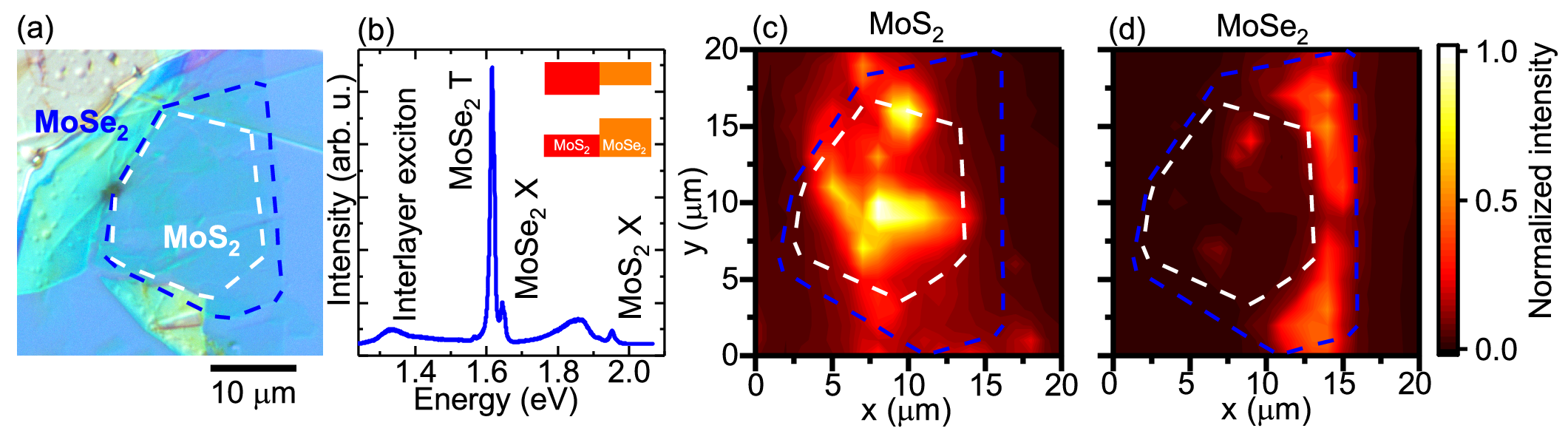
We show a micrograph of the fabricated heterostructure in Fig. 1(a). It consists of a monolayer MoSe2 flake, indicated by a blue dashed line, partially covered by a MoS2 monolayer (white dashed line). The nominal angle between the MoS2 and MoSe2 crystal axis is . Second harmonic spectroscopy confirmed that the actual stacking angle is , as discussed in the Supporting Information. Both layers are fully encapsulate in hBN and this van der Waals stack is deposited on a SiO2 substrate. A more detailed description of the fabrication procedure is provided in Methods. Additional microscope images of the flakes used to prepare the heterostructure are shown in the Supporting Information. A representative, broad range PL spectrum of our heterostructure at K is presented in Fig. 1(b). The peaks at and 1.644 eV arise from the radiative recombination of the intralayer trion and exciton of MoSe2, respectively. The weaker PL peaks centered at and are assigned to the recombination of neutral excitons and to excitonic complexes bound to defects in MoS2 48, 5, respectively. The low energy peak at 1.37 eV stems from the interlayer exciton emission, formed due to the spatial separation of charge carriers in a type II heterostructure, as schematically shown in the inset of Fig. 1(b) 31, 32. In this work, we focus on the properties of intralayer excitons. PL intensity maps of intralayer MoS2 and MoSe2 are presented in Fig. 1(c,d), respectively. The MoSe2 PL intensity of Fig. 1(d) is suppressed in the heterostructure area, due to the interlayer charge transfer 49, 50. The strongly modified optical properties in the heterostructure area are an indication of a good coupling between the layers, characteristic for stacking angle 51.
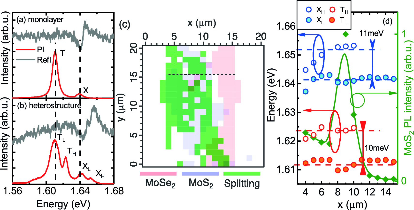
On a fully hBN-encaspulated MoSe2 monolayer, the PL spectrum consists of two peaks, attributed to charged and neutral exciton (see Fig. 2(a)). In contrast, the MoSe2 exciton and trion PL from the heterostructure region reveals a double peak structure, as shown in Fig. 2(b). We label these features X (T) and X (T), to refer to higher and lower energy transition of the exciton (trion). A similar double structure is also observed for the MoS2 free exciton emission (see Supporting Information). Importantly, the splitting of the exciton is also visible in the reflectivity spectrum of Fig. 2(b), unequivocally demonstrating that it is related to a free exciton transition rather than to the emission from excitons bound to defects. The presence of a double PL peak in the heterostructure region is consistent with the expected effect of the moiré pattern on the intralayer excitonic complexes. According to theoretical predictions, the stacking of two lattice mismatched TMD monolayers induces a spatially periodic fluctuation of the potential, felt by the excitons, 39, 40, 44, 45 with local minima related to different atomic registries 39. The period of the moiré pattern is in the range of a few to tens of nanometers (see Supporting Information for a discussion specific to our heterostructure). Therefore, the spatial resolution of our far field optical measurements is not sufficient to resolve the spatial variation of the emission energy of excitons located at different potential minima. Nevertheless, the emission from different optically active minima of the moiré pattern can be spectrally resolved in our high quality sample. The double structure of the exciton and trion peaks is consistently observed only in the heterostructure, while it is completely absent in monolayer regions. This is summarized in Fig. 2(c), where the spatial map highlights the areas where the splitting is observed. To verify that the observed splitting is a direct consequence of the moiré pattern, we prepared two control samples (presented in Supporting Information), which consist of MoS2/MoSe2 heterostructures with stacking angles of and . In former sample, the period of the moiré pattern is significantly smaller than the spatial extension of the intralayer exciton wave function and, as expected, we did not observe any splitting in the PL spectrum of the MoSe2 exciton or trion. In latter sample, we systematically observe the splitting of the exciton and trion PL peaks of MoSe2, whenever the excitation is performed within the heterostructure area. This is consistent with theoretical predictions 39, and with the long range spatial period of the moiré pattern formed in the case of and stacking angle (see Supporting Information).
In Fig. 2(d), we show the spatial variation of the exciton and trion PL energy along the dashed line crossing the heterostructure in Fig. 2(c). The slice starts and ends at positions on the sample where PL is observed. A direct comparison of the spectrum measured in the heterostructure region with one measured outside (see Fig. 2(a,b)) reveals that the double structure results from the appearance of a new energy peak on the high energy side of the main exciton and trion emission. The energies of the emission lines observed in isolated monolayers are nearly identical to the X and T lines observed in the heterostructure, as highlighted by the vertical lines in Fig. 2(a,b). This is in agreement with the prediction that the exciton states related to the moiré pattern should appear as peaks on the high energy side of the main PL peaks 39, 45. This observation, along with the fact that the double peak structure appears over a vast area in the heterostructure and not only at its edges 15, allows us to rule out the variation of the dielectric screening related to the presence of the MoS2 monolayer as the origin of the observed doublet structure. Since the dielectric constant of MoS2 is higher than that of hBN 52, a dielectric screening effect would lead to the appearance of lower energy peaks when the excitation is performed on the heterostructure 15. We also exclude a strain-related origin of the new peak by noting that the red shift of the A mode of MoSe2 in the heterostructure would suggest tensile strain of MoSe2 comprised in the heterostructure, which is not compatible with the appearance of a high energy peak in the PL spectrum 53, 54, 55 (see Supporting Information for more details). Finally, the observed energy scale of the PL peaks splitting (–) is in agreement with the energy scale of potential variations predicted for the related MoS2/WSe2 heterostructure 39.
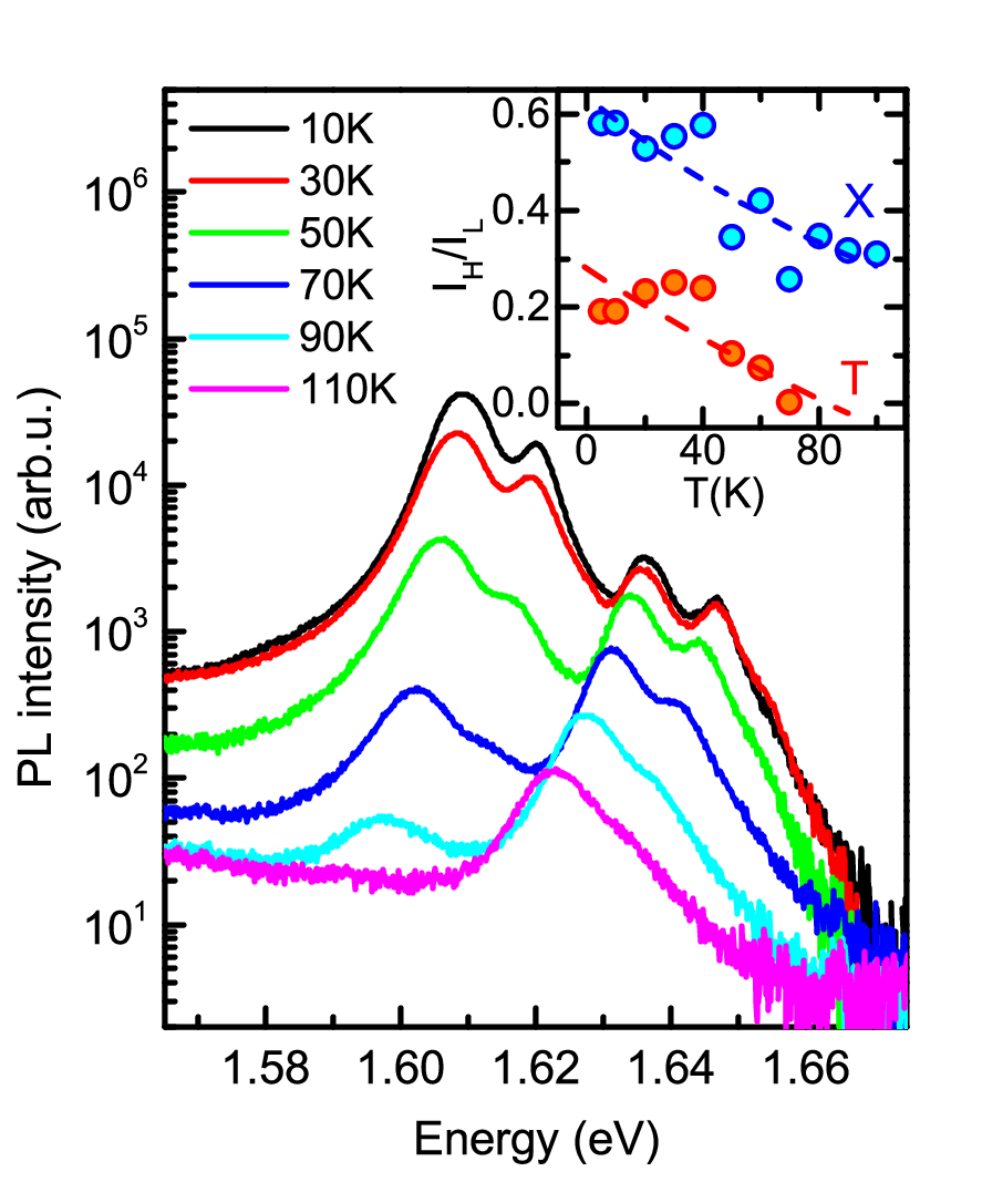
In Fig. 3, we summarize the temperature dependence of the MoSe2 PL measured on the heterostructure. As for all Mo-based TMDs, we observe a decrease of the PL intensity with increasing temperature 56. We notice in particular a faster decrease of the intensity of the trion PL, which can be no longer resolved at temperatures larger than 48, consistent with the smaller binding energy of this complex as compared to the exciton. Concerning the states split by the moiré potential, the intensity of the high energy peaks X and T decreases more rapidly than that of the low energy peaks. For temperatures higher than , corresponding to a thermal energy of , the X and T features are no longer resolved. This is illustrated in the inset of Fig. 3, where we plot the ratio of the intensities of the high energy peaks normalized by the intensities of the corresponding low energy peaks . The faster quenching of the X and T emission further supports the moiré pattern as the origin of the trion and exciton doublet. A smaller confinement is expected for the higher energy states 39, hence with increasing thermal energy these excitons can be detrapped more easily via thermally activated phonon scattering out of the minima of the moiré potential. From the temperature dependence of the intensity of X, an activation energy of can be extracted (see Supporting Information). This value compares to the depth of the moiré potential for intralayer excitons of 12–, depending on the stacking of the heterobilayer 39. This behaviour is fully consistent with the observation of a more rapid thermal quenching of the PL of high energy moiré states observed in the interlayer exciton 57.
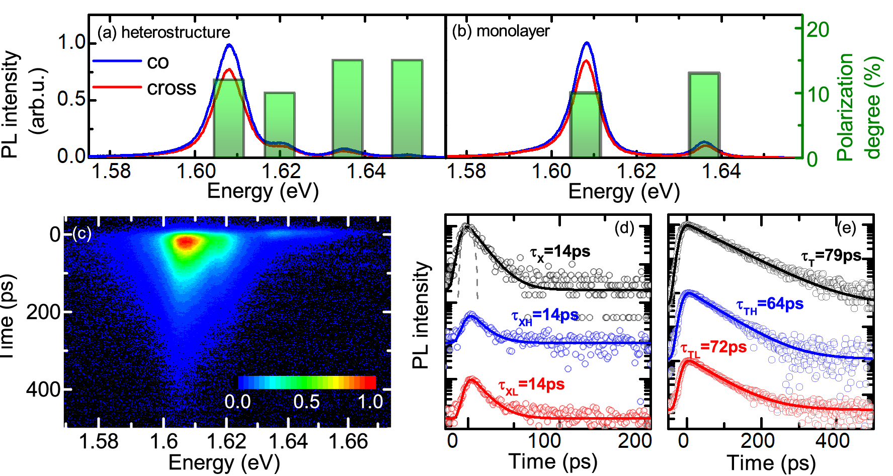
We investigated the valley polarization properties of the intralayer MoSe2 excitons by exciting the PL with circularly polarized light and detecting the co-polarized and cross-polarized circular polarization PL components. We show the PL spectra of the isolated monolayer and of the monolayer comprised in a heterostructure in Fig. 4(a,b). The degree of circular polarization of the PL, , is always positive (see green bars in Fig. 4). The degree of circular polarization is very similar for the heterostructure and monolayer regions and amounts to about 10% and 13% for the trion and the exciton, respectively. There is no significant difference between the polarization of high and low energy transitions in heterostructure. This suggests that, consistent with theoretical predictions 39, the selection rules for the intralayer exciton transitions are not influenced by the presence of the moiré pattern, thus all transitions have the same polarization. This can be explained by considering that the rotational symmetry of the transitions does not change in the plane of the monolayers, in contrast to the interlayer transition for which the helicity of the emitted light varies across the moiré pattern 39, 44. The observed significant polarization is surprising considering that we excite far from excitonic transitions of MoSe2 58, 59, 60, 48. This effect might be related to the encapsulation in hBN because we observe a similar degree of circular polarization in both the heterostructure and monolayer regions, although the exact reason the relatively high degree of polarization after encapsulation requires additional investigation.
Finally, we investigate the dynamics of the trion and exciton in MoSe2. The spectrally resolved temporal evolution of the PL measured in the heterostructure area is shown in Fig. 4(c). Similar data acquired on an isolated MoSe2 monolayer is shown in the Supporting Information. In the streak image of Fig. 4(c), the four PL peaks are well resolved, with the dynamics of the excitonic transition being significantly faster than those of the trions. To obtain more quantitative information, we extract the decay curves corresponding to MoSe2 trion and exciton transitions in monolayer and heterostructure regions in Fig. 4(d,e), respectively. PL decays of all trion and exciton species can be fitted well using a single exponential, convoluted with a Gaussian curve to account for the instrument response function of the system. From this fitting, we extract the PL life times. There are no significant differences between PL decay times in the monolayer and heterostructure areas or between X (T) and X (T) transitions. For the exciton transitions, the PL decay time is ps, while for the trion it is ps. We notice, however, that the PL decay time of the exciton is close to the resolution of our system, therefore the dynamics of the two exciton states might be slightly different. The faster decay of the high energy trion is consistent with the observation on the dynamics of high energy interlayer exciton states in a moiré potential, where this behaviour has been attributed to the possible relaxation of high energy states to the low energy states 57.
The overall similar decay times of the high and low energy transitions suggest that the moiré potential does not affect significantly the oscillator strength of the transitions. This can be understood as a result of the slow spatial variation of moiré potential (a few to tens of nm, depending on the stacking angle and the lattice mismatch of the heterobilayer) compared to the exciton size in TMD monolayers ( nm) 9, 61. Therefore, the wave function of intralayer excitons is not significantly affected by the confinement induced by the moiré pattern. Interestingly, despite a clear drop of the PL intensity in the heterostructure area (Fig. 1), the decay times of the trion and exciton PL are very similar to those observed in monolayer regions. This indicates that the charge transfer between the layers occurs immediately after excitation and is effective only for hot carriers, in agreement with previous pump probe measurements 49. The observed PL is related to thermalized excitons and the unchanged decay times show that they are not affected by the interlayer transfer. This might be the result of the weak localization potential induced by the moiré pattern. A larger intensity of the interlayer exciton PL has been observed in MoSe2/MoS2 heterostructures 31 with increasing temperature. This is probably the hallmark of the thermal activation of excitons from shallow traps, represented by the moiré potential, followed by interlayer transfer. However, further studies are needed to clarify this aspect, notably to distinguish it from a possible indirect character in k-space of the interlayer transitions 30, 62.
In conclusion, we have demonstrated the impact of the moiré pattern formed in a MoS2/MoSe2 heterostructure on the optical spectra of the intralayer exciton species. The potential fluctuations resulting from locally different atomic registries split the trion and exciton transitions of MoSe2 and MoS2 into two peaks related to optically active local minima of the moiré potential. The nature of these doublets has been confirmed by detailed spatial mapping of the PL and by the temperature dependence of their PL. Polarization resolved measurements reveal that the selection rules of the transitions do not change with respect to the case of isolated monolayers. The PL dynamics show that moiré induced potential does not change significantly the oscillator strength of the transitions. However, the moiré potential may be responsible for the suppression of the interlayer transfer of thermalized excitons. All of the results presented are in agreement with the theoretically predicted influence of moiré pattern on intralayer excitons in transition metal dichalcogenides.
Methods
Sample preparation. The samples have been prepared by all-dry deterministic transfer of mechanically exfoliated flakes 63, 64. hBN flakes have been exfoliated from commercially available hBN powder (Momentive, Polartherm grade PT110) using Nitto tape (Nitto Denko corp. SPV 224). MoS2 and MoSe2 flakes have been also exfoliated with Nitto tape from naturally occurring molybdenite mineral (Molly Hill mine, Quebec, Canada) and synthetic bulk MoSe2 grown by chemical vapour transport. The flakes cleaved from the bulk source of material are transferred onto a Gelfilm (WF x4 6.0 mil by Gelpak) that is used as a viscoelastic stamp to perform the deterministic transfer. MoS2 and MoSe2 monolayers are selected from their transmittance and reflection spectra prior to their transfer 65. Monolayers with large faceted edges were used for the assembly of the heterostructures. The straight edges of the MoS2 and MoSe2 were aligned with accuracy better than during the transfer.
Optical spectroscopy. For optical measurements, the sample was mounted on the cold finger of a helium flow cryostat with a quartz optical window. Unless stated otherwise, all measurements have been performed at K. Time resolved PL measurements were performed using a CW frequency doubled solid state laser emitting at 532 nm. The circularly polarization resolved PL was excited with the frequency-doubled output of an optical parametric oscillator (OPO), synchronously pumped by a mode-locked Ti:sapphire laser and tuned to . The temporal pulse width is typically , with a repetition rate of . The instrument response function of the system, shown in Fig. 4(d), has a half width at half maximum of . The excitation laser beam was focused on the sample using a microscope objective with a numerical aperture of 0.55, giving a spot size of approximately diameter. The excitation power used for time-integrated measurements was . The emitted PL was collected through the same objective and directed to a spectrometer equipped with a liquid nitrogen cooled charge-coupled device (CCD) camera. For time-resolved measurements, the excitation was provided by the OPO tuned to , using an average power of . The collected signal was spectrally dispersed using a monochromator and detected using a streak camera. Second harmonic measurements were performed in a similar setup. The Ti:sapphire laser was used as the excitation source. The laser light was polarized via a broadband polarizer and a halfwave plate was used to control the direction of the linear polarization of the fundamental wave. The laser was focused onto the sample using the same microscope objective used for PL measurements. The same set of halfwave plate and linear polarizer were used to analyze the polarization of the second harmonic signal, thus insuring that only the component of the second harmonic parallel to the polarization of the excitation was detected. The second harmonic signal was separated by the fundamental component by making use of a shortpass filter. The signal was finally detected by the spectrometer combined with the CCD.
Micrograph of different stages of preparation of the van der Waals stack, second harmonic spectroscopy of the heterostructure presented in the main text, period of moiré pattern as a function of the stacking angle, PL spectra of additional devices with and stacking angle, activation energy of high energy exciton peak, Raman spectra of isolated MoSe2 and MoSe2 in a heterostructure, maps of the energy splitting of MoSe2 exciton and trion, low temperature PL spectrum of MoS2 with split exciton peak, and time resolved PL of isolated MoSe2.
This work was partially supported by BLAPHENE and STRABOT projects, which received funding from the IDEX Toulouse, Emergence program, “Programme des Investissements d’Avenir” under the program ANR-11-IDEX-0002-02, reference ANR-10-LABX-0037-NEXT. N.Z. holds a fellowship from the China Scholarship Council (CSC). M.B. appreciates support from the Polish Ministry of Science and Higher Education within the Mobilnosc Plus program (grant no. 1648/MOB/V/2017/0). This project has also received funding from the European Research Council (ERC) under the European Union’s Horizon 2020 research and innovation programme (grant agreement no. 755655, ERC-StG 2017 project 2D-TOPSENSE) and from the EU Graphene Flagship funding (Grant Graphene Core 2, 785219).
References
- Geim and Grigorieva 2013 Geim, A. K.; Grigorieva, I. V. Van der Waals heterostructures. Nature 2013, 499, 419–425
- Novoselov et al. 2016 Novoselov, K.; Mishchenko, A.; Carvalho, A.; Neto, A. C. 2D materials and van der Waals heterostructures. Science 2016, 353, aac9439
- Dong and Kuljanishvili 2017 Dong, R.; Kuljanishvili, I. Progress in fabrication of transition metal dichalcogenides heterostructure systems. Journal of Vacuum Science & Technology B, Nanotechnology and Microelectronics: Materials, Processing, Measurement, and Phenomena 2017, 35, 030803
- Zhou et al. 2018 Zhou, X.; Hu, X.; Yu, J.; Liu, S.; Shu, Z.; Zhang, Q.; Li, H.; Ma, Y.; Xu, H.; Zhai, T. 2D Layered Material-Based van der Waals Heterostructures for Optoelectronics. Advanced Functional Materials 2018, 28, 1706587
- Cadiz et al. 2017 Cadiz, F.; Courtade, E.; Robert, C.; Wang, G.; Shen, Y.; Cai, H.; Taniguchi, T.; Watanabe, K.; Carrere, H.; Lagarde, D.; Manca, M.; Amand, T.; Renucci, P.; Tongay, S.; Marie, X.; Urbaszek, B. Excitonic linewidth approaching the homogeneous limit in MoS 2-based van der Waals heterostructures. Physical Review X 2017, 7, 021026
- Fallahazad et al. 2016 Fallahazad, B.; Movva, H. C.; Kim, K.; Larentis, S.; Taniguchi, T.; Watanabe, K.; Banerjee, S. K.; Tutuc, E. Shubnikov–de Haas oscillations of high-mobility holes in monolayer and bilayer WSe 2: Landau level degeneracy, effective mass, and negative compressibility. Physical Review Letters 2016, 116, 086601
- Robert et al. 2018 Robert, C.; Semina, M.; Cadiz, F.; Manca, M.; Courtade, E.; Taniguchi, T.; Watanabe, K.; Cai, H.; Tongay, S.; Lassagne, B.; Renucci, P.; Amand, T.; Marie, X.; Glazov, M. M.; Urbaszek, B. Optical spectroscopy of excited exciton states in MoS2 monolayers in van der Waals heterostructures. Physical Review Materials 2018, 2, 011001
- Manca et al. 2017 Manca, M.; Glazov, M.; Robert, C.; Cadiz, F.; Taniguchi, T.; Watanabe, K.; Courtade, E.; Amand, T.; Renucci, P.; Marie, X.; Wang, G.; Urbaszek, B. Enabling valley selective exciton scattering in monolayer WSe2 through upconversion. Nature Communications 2017, 8, 14927
- Stier et al. 2018 Stier, A. V.; Wilson, N. P.; Velizhanin, K. A.; Kono, J.; Xu, X.; Crooker, S. A. Magnetooptics of Exciton Rydberg States in a Monolayer Semiconductor. Physical Review Letters 2018, 120, 057405
- Chen et al. 2018 Chen, S.-Y.; Goldstein, T.; Tong, J.; Taniguchi, T.; Watanabe, K.; Yan, J. Superior Valley Polarization and Coherence of 2s Excitons in Monolayer WSe2. Physical Review Letters 2018, 120, 046402
- Xu et al. 2017 Xu, S.; Shen, J.; Long, G.; Wu, Z.; Bao, Z.-q.; Liu, C.-C.; Xiao, X.; Han, T.; Lin, J.; Wu, Y.; Lu, H.; Hou, J.; An, L.; Wang, Y.; Cai, Y.; Ho, K. M.; He, Y.; Lortz, R.; Zhang, F.; Wang, N. Odd-Integer Quantum Hall States and Giant Spin Susceptibility in p-Type Few-Layer WSe2. Physical Review Letters 2017, 118, 067702
- Movva et al. 2017 Movva, H. C.; Fallahazad, B.; Kim, K.; Larentis, S.; Taniguchi, T.; Watanabe, K.; Banerjee, S. K.; Tutuc, E. Density-Dependent Quantum Hall States and Zeeman Splitting in Monolayer and Bilayer WSe2. Physical Review Letters 2017, 118, 247701
- Bandurin et al. 2017 Bandurin, D. A.; Tyurnina, A. V.; Geliang, L. Y.; Mishchenko, A.; Zólyomi, V.; Morozov, S. V.; Kumar, R. K.; Gorbachev, R. V.; Kudrynskyi, Z. R.; Pezzini, S.; Kovalyuk, Z. D.; Zeitler, U.; Novoselov, K. S.; Patanè, A.; Eaves, L.; Grigoreva, I. V.; Falko, V. I.; Geim, A. K.; Cao, Y. High electron mobility, quantum Hall effect and anomalous optical response in atomically thin InSe. Nature Nanotechnology 2017, 12, 223–227
- Wu et al. 2016 Wu, Z.; Xu, S.; Lu, H.; Khamoshi, A.; Liu, G.-B.; Han, T.; Wu, Y.; Lin, J.; Long, G.; He, Y.; He, Y.; Cai, Y.; Yao, Y.; Zhang, F.; Wang, N. Even–odd layer-dependent magnetotransport of high-mobility Q-valley electrons in transition metal disulfides. Nature Communications 2016, 7, 12955
- Raja et al. 2017 Raja, A.; Chaves, A.; Yu, J.; Arefe, G.; Hill, H. M.; Rigosi, A. F.; Berkelbach, T. C.; Nagler, P.; Schüller, C.; Korn, T.; Nuckolls, C.; Hone, J.; Brus, L. E.; Heinz, T. F.; Reichman, D. R.; Chernikov, A. Coulomb engineering of the bandgap and excitons in two-dimensional materials. Nature Communications 2017, 8, 15251
- Xiao et al. 2012 Xiao, D.; Liu, G.-B.; Feng, W.; Xu, X.; Yao, W. Coupled spin and valley physics in monolayers of MoS2 and other group-VI dichalcogenides. Physical Review Letters 2012, 108, 196802
- Xu et al. 2014 Xu, X.; Yao, W.; Xiao, D.; Heinz, T. F. Spin and pseudospins in layered transition metal dichalcogenides. Nature Physics 2014, 10, 343–350
- Wang et al. 2012 Wang, Q. H.; Kalantar-Zadeh, K.; Kis, A.; Coleman, J. N.; Strano, M. S. Electronics and optoelectronics of two-dimensional transition metal dichalcogenides. Nature Nanotechnology 2012, 7, 699–712
- Mak et al. 2012 Mak, K. F.; He, K.; Shan, J.; Heinz, T. F. Control of valley polarization in monolayer MoS2 by optical helicity. Nature Nanotechnology 2012, 7, 494–498
- Zeng et al. 2012 Zeng, H.; Dai, J.; Yao, W.; Xiao, D.; Cui, X. Valley polarization in MoS2 monolayers by optical pumping. Nature Nanotechnology 2012, 7, 490–493
- Lagarde et al. 2014 Lagarde, D.; Bouet, L.; Marie, X.; Zhu, C. R.; Liu, B. L.; Amand, T.; Tan, P. H.; Urbaszek, B. Carrier and polarization dynamics in monolayer MoS2. Physical Review Letters 2014, 112, 047401
- Wang et al. 2014 Wang, G.; Bouet, L.; Lagarde, D.; Vidal, M.; Balocchi, A.; Amand, T.; Marie, X.; Urbaszek, B. Valley dynamics probed through charged and neutral exciton emission in monolayer WSe2. Physical Review B 2014, 90, 075413
- Robert et al. 2016 Robert, C.; Lagarde, D.; Cadiz, F.; Wang, G.; Lassagne, B.; Amand, T.; Balocchi, A.; Renucci, P.; Tongay, S.; Urbaszek, B.; Marie, X. Exciton radiative lifetime in transition metal dichalcogenide monolayers. Physical Review B 2016, 93, 205423
- Wang et al. 2015 Wang, G.; Palleau, E.; Amand, T.; Tongay, S.; Marie, X.; Urbaszek, B. Polarization and time-resolved photoluminescence spectroscopy of excitons in MoSe2 monolayers. Applied Physics Letters 2015, 106, 112101
- Zhu et al. 2014 Zhu, C. R.; Zhang, K.; Glazov, M.; Urbaszek, B.; Amand, T.; Ji, Z. W.; Liu, B. L.; Marie, X. Exciton valley dynamics probed by Kerr rotation in WSe2 monolayers. Physical Review B 2014, 90, 161302
- Kang et al. 2013 Kang, J.; Tongay, S.; Zhou, J.; Li, J.; Wu, J. Band offsets and heterostructures of two-dimensional semiconductors. Applied Physics Letters 2013, 102, 012111
- Rivera et al. 2015 Rivera, P.; Schaibley, J. R.; Jones, A. M.; Ross, J. S.; Wu, S.; Aivazian, G.; Klement, P.; Seyler, K.; Clark, G.; Ghimire, N. J.; Yan, J.; Mandrus, D. G.; Yao, W.; Xu, X. Observation of long-lived interlayer excitons in monolayer MoSe2-WSe2 heterostructures. Nature Communications 2015, 6, 6242
- Rivera et al. 2016 Rivera, P.; Seyler, K. L.; Yu, H.; Schaibley, J. R.; Yan, J.; Mandrus, D. G.; Yao, W.; Xu, X. Valley-polarized exciton dynamics in a 2D semiconductor heterostructure. Science 2016, 351, 688–691
- Nagler et al. 2017 Nagler, P.; Plechinger, G.; Ballottin, M. V.; Mitioglu, A.; Meier, S.; Paradiso, N.; Strunk, C.; Chernikov, A.; Christianen, P. C.; Schüller, C.; Korn, T. Interlayer exciton dynamics in a dichalcogenide monolayer heterostructure. 2D Materials 2017, 4, 025112
- Miller et al. 2017 Miller, B.; Steinhoff, A.; Pano, B.; Klein, J.; Jahnke, F.; Holleitner, A.; Wurstbauer, U. Long-lived direct and indirect interlayer excitons in van der Waals heterostructures. Nano Letters 2017, 17, 5229–5237
- Baranowski et al. 2017 Baranowski, M.; Surrente, A.; Klopotowski, L.; Urban, J.; Zhang, N.; Maude, D. K.; Wiwatowski, K.; Mackowski, S.; Kung, Y.-C.; Dumcenco, D.; Kis, A.; Plochocka, P. Probing the Interlayer Exciton Physics in a MoS2/MoSe2/MoS2 van der Waals Heterostructure. Nano Letters 2017, 17, 6360–6365
- Surrente et al. 2018 Surrente, A.; Klopotowski, Ł.; Zhang, N.; Baranowski, M.; Mitioglu, A.; Ballottin, M. V.; Christianen, P. C.; Dumcenco, D.; Kung, Y.-C.; Maude, D. K.; Kis, A.; Plochocka, P. Intervalley Scattering of Interlayer Excitons in a MoS2/MoSe2/MoS2 Heterostructure in High Magnetic Field. Nano Letters 2018, 18, 3994–4000
- Hanbicki et al. 2018 Hanbicki, A. T.; Chuang, H.-J.; Rosenberger, M. R.; Hellberg, C. S.; Sivaram, S. V.; McCreary, K. M.; Mazin, I. I.; Jonker, B. T. Double Indirect Interlayer Exciton in a MoSe2/WSe2 van der Waals Heterostructure. ACS Nano 2018, 12, 4719–4726
- Hsu et al. 2018 Hsu, W.-T.; Lu, L.-S.; Wu, P.-H.; Lee, M.-H.; Chen, P.-J.; Wu, P.-Y.; Chou, Y.-C.; Jeng, H.-T.; Li, L.-J.; Chu, M.-W.; Chang, W.-H. Negative circular polarization emissions from WSe2/MoSe2 commensurate heterobilayers. Nature Communications 2018, 9, 1356
- Park et al. 2008 Park, C.-H.; Yang, L.; Son, Y.-W.; Cohen, M. L.; Louie, S. G. Anisotropic behaviours of massless Dirac fermions in graphene under periodic potentials. Nature Physics 2008, 4, 213–217
- Xue et al. 2011 Xue, J.; Sanchez-Yamagishi, J.; Bulmash, D.; Jacquod, P.; Deshpande, A.; Watanabe, K.; Taniguchi, T.; Jarillo-Herrero, P.; LeRoy, B. J. Scanning tunnelling microscopy and spectroscopy of ultra-flat graphene on hexagonal boron nitride. Nature Materials 2011, 10, 282–285
- Yankowitz et al. 2012 Yankowitz, M.; Xue, J.; Cormode, D.; Sanchez-Yamagishi, J. D.; Watanabe, K.; Taniguchi, T.; Jarillo-Herrero, P.; Jacquod, P.; LeRoy, B. J. Emergence of superlattice Dirac points in graphene on hexagonal boron nitride. Nature Physics 2012, 8, 382–386
- Ponomarenko et al. 2013 Ponomarenko, L.; Gorbachev, R.; Yu, G.; Elias, D.; Jalil, R.; Patel, A.; Mishchenko, A.; Mayorov, A.; Woods, C.; Wallbank, J.; Mucha-Kruszynski, M.; Piot, B. A.; Potemski, M.; Grigorieva, I. V.; Novoselov, K. S.; Guinea, F.; Falko, V. I.; K, G. A. Cloning of Dirac fermions in graphene superlattices. Nature 2013, 497, 594–597
- Yu et al. 2017 Yu, H.; Liu, G.-B.; Tang, J.; Xu, X.; Yao, W. Moiré excitons: From programmable quantum emitter arrays to spin-orbit–coupled artificial lattices. Science Advances 2017, 3, e1701696
- Zhang et al. 2017 Zhang, C.; Chuu, C.-P.; Ren, X.; Li, M.-Y.; Li, L.-J.; Jin, C.; Chou, M.-Y.; Shih, C.-K. Interlayer couplings, Moiré patterns, and 2D electronic superlattices in MoS2/WSe2 hetero-bilayers. Science Advances 2017, 3, e1601459
- Hunt et al. 2013 Hunt, B.; Sanchez-Yamagishi, J.; Young, A.; Yankowitz, M.; LeRoy, B. J.; Watanabe, K.; Taniguchi, T.; Moon, P.; Koshino, M.; Jarillo-Herrero, P.; Ashoori, R. C. Massive Dirac fermions and Hofstadter butterfly in a van der Waals heterostructure. Science 2013, 340, 1427–1430
- Wang et al. 2016 Wang, E.; Lu, X.; Ding, S.; Yao, W.; Yan, M.; Wan, G.; Deng, K.; Wang, S.; Chen, G.; Ma, L.; Jung, J.; Fedorov, A. V.; Zhang, Y.; Zhang, G.; Zhou, S. Gaps induced by inversion symmetry breaking and second-generation Dirac cones in graphene/hexagonal boron nitride. Nature Physics 2016, 12, 1111–1115
- Dean et al. 2013 Dean, C.; Wang, L.; Maher, P.; Forsythe, C.; Ghahari, F.; Gao, Y.; Katoch, J.; Ishigami, M.; Moon, P.; Koshino, M.; Taniguchi, T.; Watanabe, K.; Shepard, K. L.; Hone, J.; Kim, P. Hofstadter’s butterfly and the fractal quantum Hall effect in moiré superlattices. Nature 2013, 497, 598–602
- Wu et al. 2018 Wu, F.; Lovorn, T.; MacDonald, A. Theory of optical absorption by interlayer excitons in transition metal dichalcogenide heterobilayers. Physical Review B 2018, 97, 035306
- Wu et al. 2017 Wu, F.; Lovorn, T.; Macdonald, A. H. Topological Exciton Bands in Moiré Heterojunctions. Physical Review Letters 2017, 118, 147401
- Pan et al. 2018 Pan, Y.; Fölsch, S.; Nie, Y.; Waters, D.; Lin, Y.-C.; Jariwala, B.; Zhang, K.; Cho, K.; Robinson, J. A.; Feenstra, R. M. Quantum-Confined Electronic States arising from Moiré Pattern of MoS2-WSe2 Heterobilayers. Nano Letters 2018, 18, 1849–1855
- Ciarrocchi et al. 2018 Ciarrocchi, A.; Unuchek, D.; Avsar, A.; Watanabe, K.; Taniguchi, T.; Kis, A. Control of interlayer excitons in two-dimensional van der Waals heterostructures. arXiv preprint arXiv:1803.06405 2018,
- Surrente et al. 2017 Surrente, A.; Dumcenco, D.; Yang, Z.; Kuc, A.; Jing, Y.; Heine, T.; Kung, Y.-C.; Maude, D. K.; Kis, A.; Plochocka, P. Defect Healing and Charge Transfer-Mediated Valley Polarization in MoS2/MoSe2/MoS2 Trilayer van der Waals Heterostructures. Nano Letters 2017, 17, 4130–4136
- Ceballos et al. 2014 Ceballos, F.; Bellus, M. Z.; Chiu, H.-Y.; Zhao, H. Ultrafast charge separation and indirect exciton formation in a MoS2–MoSe2 van der Waals heterostructure. ACS Nano 2014, 8, 12717–12724
- Chen et al. 2016 Chen, H.; Wen, X.; Zhang, J.; Wu, T.; Gong, Y.; Zhang, X.; Yuan, J.; Yi, C.; Lou, J.; Ajayan, P. M.; Zhuang, W.; Zhang, G.; Zheng, J. Ultrafast formation of interlayer hot excitons in atomically thin MoS2/WS2 heterostructures. Nature Communications 2016, 7, 12512
- Wang et al. 2016 Wang, K.; Huang, B.; Tian, M.; Ceballos, F.; Lin, M.-W.; Mahjouri-Samani, M.; Boulesbaa, A.; Puretzky, A. A.; Rouleau, C. M.; Yoon, M.; Zhao, H.; Xiao, K.; Duscher, G.; Geohegan, D. B. Interlayer coupling in twisted WSe2/WS2 bilayer heterostructures revealed by optical spectroscopy. ACS Nano 2016, 10, 6612–6622
- Laturia et al. 2018 Laturia, A.; Van de Put, M. L.; Vandenberghe, W. G. Dielectric properties of hexagonal boron nitride and transition metal dichalcogenides: from monolayer to bulk. npj 2D Materials and Applications 2018, 2, 6
- Conley et al. 2013 Conley, H. J.; Wang, B.; Ziegler, J. I.; Haglund Jr, R. F.; Pantelides, S. T.; Bolotin, K. I. Bandgap engineering of strained monolayer and bilayer MoS2. Nano letters 2013, 13, 3626–3630
- Lloyd et al. 2016 Lloyd, D.; Liu, X.; Christopher, J. W.; Cantley, L.; Wadehra, A.; Kim, B. L.; Goldberg, B. B.; Swan, A. K.; Bunch, J. S. Band gap engineering with ultralarge biaxial strains in suspended monolayer MoS2. Nano Letters 2016, 16, 5836–5841
- Castellanos-Gomez et al. 2013 Castellanos-Gomez, A.; Roldán, R.; Cappelluti, E.; Buscema, M.; Guinea, F.; van der Zant, H. S.; Steele, G. A. Local strain engineering in atomically thin MoS2. Nano letters 2013, 13, 5361–5366
- Zhang et al. 2015 Zhang, X.-X.; You, Y.; Zhao, S. Y. F.; Heinz, T. F. Experimental evidence for dark excitons in monolayer WSe 2. Physical Review Letters 2015, 115, 257403
- Tran et al. 2018 Tran, K.; Moody, G.; Wu, F.; Lu, X.; Choi, J.; Singh, A.; Embley, J.; Zepeda, A.; Campbell, M.; Kim, K.; Rai, A.; Autry, T.; Sanchez, D. A.; Taniguchi, T.; Watanabe, K.; Lu, N.; Banerjee, S. K.; Tutuc, E.; Yang, L.; MacDonal, A. H.; Silverman, K. L.; Li, X. Moiré Excitons in Van der Waals Heterostructures. arXiv preprint arXiv:1807.03771 2018,
- Wang et al. 2015 Wang, G.; Palleau, E.; Amand, T.; Tongay, S.; Marie, X.; Urbaszek, B. Polarization and time-resolved photoluminescence spectroscopy of excitons in MoSe2 monolayers. Applied Physics Letters 2015, 106, 112101
- Kioseoglou et al. 2016 Kioseoglou, G.; Hanbicki, A. T.; Currie, M.; Friedman, A. L.; Jonker, B. T. Optical polarization and intervalley scattering in single layers of MoS2 and MoSe2. Scientific Reports 2016, 6, 25041
- Baranowski et al. 2017 Baranowski, M.; Surrente, A.; Maude, D.; Ballottin, M.; Mitioglu, A.; Christianen, P.; Kung, Y.; Dumcenco, D.; Kis, A.; Plochocka, P. Dark excitons and the elusive valley polarization in transition metal dichalcogenides. 2D Materials 2017, 4, 025016
- Stier et al. 2016 Stier, A. V.; Wilson, N. P.; Clark, G.; Xu, X.; Crooker, S. A. Probing the influence of dielectric environment on excitons in monolayer WSe2: insight from high magnetic fields. Nano Letters 2016, 16, 7054–7060
- Kunstmann et al. 2018 Kunstmann, J.; Mooshammer, F.; Nagler, P.; Chaves, A.; Stein, F.; Paradiso, N.; Plechinger, G.; Strunk, C.; Schüller, C.; Seifert, G.; Reichman, D. R.; Korn, T. Momentum-space indirect interlayer excitons in transition metal dichalcogenide van der Waals heterostructures. Nature Physics 2018, 14, 801–805
- Castellanos-Gomez et al. 2014 Castellanos-Gomez, A.; Buscema, M.; Molenaar, R.; Singh, V.; Janssen, L.; Van Der Zant, H. S.; Steele, G. A. Deterministic transfer of two-dimensional materials by all-dry viscoelastic stamping. 2D Materials 2014, 1, 011002
- Frisenda et al. 2018 Frisenda, R.; Navarro-Moratalla, E.; Gant, P.; De Lara, D. P.; Jarillo-Herrero, P.; Gorbachev, R. V.; Castellanos-Gomez, A. Recent progress in the assembly of nanodevices and van der Waals heterostructures by deterministic placement of 2D materials. Chemical Society Reviews 2018, 47, 53–68
- Frisenda et al. 2017 Frisenda, R.; Niu, Y.; Gant, P.; Molina-Mendoza, A. J.; Schmidt, R.; Bratschitsch, R.; Liu, J.; Fu, L.; Dumcenco, D.; Kis, A.; Perez De Lara, D.; Castellanos-Gomez, A. Micro-reflectance and transmittance spectroscopy: a versatile and powerful tool to characterize 2D materials. Journal of Physics D: Applied Physics 2017, 50, 074002
![[Uncaptioned image]](/html/1811.03408/assets/TOCfigure.png)