Present address: ]London Centre for Nanotechnology, UCL, London WC1H 0AH, United Kingdom
Quantitative modeling of superconducting planar resonators with improved field homogeneity for electron spin resonance
Abstract
We present three designs for planar superconducting microwave resonators for electron spin resonance (ESR) experiments. We implement finite element simulations to calculate the resonance frequency and quality factors as well as the three-dimensional microwave magnetic field distribution of the resonators. One particular resonator design offers an increased homogeneity of the microwave magnetic field while the other two show a better confinement of the mode volume. We extend our model simulations to calculate the collective coupling rate between a spin ensemble and a microwave resonator in the presence of an inhomogeneous magnetic resonator field. Continuous-wave ESR experiments of phosphorus donors in natSi demonstrate the feasibility of our resonators for magnetic resonance experiments. We extract the collective coupling rate and find a good agreement with our simulation results, corroborating our model approach. Finally, we discuss specific application cases for the different resonator designs.
I Introduction
Microwave resonators are a key part of any ESR experiment. They enhance the microwave magnetic field at the sample location and offer equally enhanced sensitivity for inductive detection of magnetization dynamicsPoole (1996); Schweiger and Jeschke (2001). While conventional ESR resonators based on three-dimensional (3D) microwave cavities provide a microwave magnetic field with high homogeneity over a large volume, they suffer from small filling factors and, in turn, a low sensitivity for small samples. Planar microresonators allow to reduce the mode volume, which, depending on the sample size and geometry, can lead to an increased filling factor and therefore an enhanced sensitivity compared to 3D cavitiesNarkowicz et al. (2005, 2008); Torrezan et al. (2009). In addition, planar resonators operated at low temperatures allow one to use superconducting materials, offering small losses and extraordinarily high quality factors. Making use of these advantages led to a plethora of planar resonator geometriesMalissa et al. (2013); Benningshof et al. (2013); Sigillito et al. (2014), applicable in several different fields of expertise. In addition, superconducting resonators have also become key components in the field of circuit quantum electrodynamics (cQED)Devoret and Schoelkopf (2013) and led to a subsequent introduction of cQED concepts in the field of magnetic resonanceWesenberg et al. (2009); Wu et al. (2010); Abe et al. (2011); Sandner et al. (2012). The quest for ultra-sensitive ESR at low temperatures has led to a range of experiments. Well-known examples are the use of parametric amplification based on superconducting quantum circuitsBienfait et al. (2016); Probst et al. (2017) or the use of quantum states as a resource to increase the signal-to-noise ratioBienfait et al. (2017). Another direction is to increase the coupling rate between a spin ensemble and the microwave resonator to enhance the read-out sensitivity of the measurements. Here, the so-called strong coupling regime has been achieved for several types of spin systems in combination with superconducting resonatorsKubo et al. (2010); Schuster et al. (2010); Amsüss et al. (2011); Probst et al. (2013); Zollitsch et al. (2015).
Despite inspring progress in ultra-sensitive ESR, so far a quantitative analysis of planar resonator designs and their suitability for achieving strong coupling and enabling straight forward coherent control of spin systems is still missing. Here, we employ finite element simulations of superconducting planar microwave resonators for calculating the spatial distribution of the microwave magnetic field of three different resonator geometries. This information is crucial to judge the performance of the resonator for the specific application. We demonstrate that these simulations can not only be used to predict the resonance frequencies and quality factors but also allow for a quantitative comparison of the magnetic field homogeneity. Additionally, the simulated magnetic field distribution enables us to calculate the expected collective coupling rate between the spin ensemble and the microwave resonator. Finally, we compare our model predictions to actual continuous-wave ESR data and find a good agreement between theory and experiment, including the modeling of power-dependent saturation effects. Here, we show that the modified power saturation is confirming the simulations of the microwave magnetic field distribution. In addition, this work compares the various resonator designs with different levels of microwave magnetic field homogeneity. This is relevant in the context of pulsed ESR experiments, as homogeneous microwave magnetic excitation fields are a key requirement for the coherent control of spin ensembles using rectangular pulse excitation schemes.
The experimental data presented in this work is recorded at a temperature of , i.e. the resonator is not in its quantum ground state. Chiorescu et al. demonstrated by numerical simulations that a transition to the classical spin-resonance mechanism occurs when the number of photons in the resonator, , is large compared to the number of spins, Chiorescu et al. (2010). However, as we will show later, this is not the case for the measurements presented in this manuscript. Our data therefore allows to compare the computed effective coupling between the microwave resonator and the spin ensemble also at Millikelvin temperatures, as the thermal spin polarization can be taken into accountZollitsch et al. (2015).
The paper is organized as follows. First, we introduce three different planar resonator designs and present important design considerations. We then introduce the concept of spin-photon coupling in the context of electron spin resonance and show how the collective coupling rate can be computed in the presence of an inhomogeneous microwave magnetic field. Subsequently, we present our simulation approach. We quantitatively analyze the field homogeneity of two of the resonator designs and show that one particular design offers an improved field homogeneity. In the following experimental section, we first confirm the feasibility of our simulation approach. The second part of the experimental section is dedicated to continuous-wave ESR experiments on an ensemble of phosphorus donors in silicon. We extract the collective coupling rate and find a good agreement between the theoretical model and the experimental data. Finally, we also model the power-dependent saturation of the collective coupling rate.
II Theoretical considerations
II.1 Microwave resonator designs
In the following, we present the sample layout and the resonator designs presented in this article. Fig. 1 (a) displays the generic design of a chip featuring a central feedline, designed in coplanar waveguide geometryWen (1969), with two connection pads at the edges of the substrate. More details and characteristic parameters are given in Section III.1.
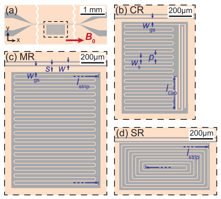
The planar microwave resonator structure is placed in proximity to a microwave feedline (dashed box). Figure 1 (b)–(d) shows the three discussed resonator designs, which are (b) a capacitively-shunted meander resonator (CR), (c) a meander resonator (MR), and (d) a spiral resonator (SR). For the MR, the capacitance is provided by the intra-line capacitance with a higher inductance to capacitance ratio than the CR. The SR design also relies on the intra-line capacitance, but provides a more homogeneous magnetic field distribution than the MR design.
The CR is a so-called lumped element microwave resonatorLindström et al. (2009); Khalil et al. (2011); Geerlings et al. (2012) where the capacitance and the inductance are most obviously visible in form of the interdigital capacitor and the meandering inductor. Nevertheless, a numeric analysis of the resonance frequency as a function of the interdigital capacitance finger length (see Fig. 4 (a)) suggests that there is a finite capacitance contained in the meandering structure for the design displayed. In consequence, the meandering resonator is the logical next step, where the interdigital capacitor is completely missing. The explicit missing capacitance is compensated by an enhanced total length of the resonator structure. An alternative viewpoint is to think of the meander resonator as a waveguide structure, where the length of the conductor supports a standing wave pattern of the microwave Wallace and Silsbee (1991). Here, the length of the meander-shaped strip of the MR and SR corresponds to half of the wavelength of the resonance frequency and thus supports this picture.
The meander shape of the CR and MR results in a counter-flow of the high-frequency currents in neighboring meandering strips. This ennables a localization of the electromagnetic field close to the surface. In addition, this also leads to a significant inhomogeneity of the microwave magnetic field in close proximity of the structure. Moreover, a fast decay of the microwave excitation field in the -direction, i.e. out of the plane of the microwave resonator (see Fig. 2 (a) and (c)) is obtained. The characteristic decay length of the field in -direction is related to the distance between adjacent wires, which is in our design. Although this can be beneficial for the measurement of ultra-thin spin samples, for most pulsed ESR experiments, using rectangular pulse excitation schemse, the large field inhomogeneity is undesired and elaborate techniques have been proposed to compensate the inhomogeneityKupce and Freeman (1995); Tannús et al. (1997); Garwood and DelaBarre (2001); Skinner et al. (2011); Spindler et al. (2012). A suitable resonator design leading to a significant reduction of the magnetic field inhomogeneity comes in the form of a spiral resonator geometry as displayed in Fig. 1 (d). Here, neighboring lines have a parallel flow of current resulting in a much better homogeneity of the field as shown in Fig. 2 (b) and (d). Note that the field extends now significantly further into the -direction and the characteristic decay length is in the same order of magnitude as the lateral dimensions of the whole resonator.
The design resonance frequency of the superconducting microwave resonators discussed here is set to a value around . This optimizes the surface impedance/losses of the structure (which increase with increasing frequencyTurneaure et al. (1991)), while keeping a reasonably high-frequency. Additionally, our experimental setup is designed to operate in the frequency band of 4–. In general, the resonance frequency of a LC-oscillator is given by with an effective inductance and capacitance . Changing the length of the capacitor finger for the CR or the total inductor length for the MR and SR allows to tune the resonance frequency to the desired value.
A further key parameter of a microwave resonator is the quality factor , which is given by , where is the loss rate of the resonator (measured as the half-width at half maximum of the resonance line). One can distinguish between internal and external losses with corresponding quality factors given by
| (1) |
The quality factors are linked to the external and internal loss rate according to and . Internal losses, including radiation, resistive and dielectric lossesGöppl et al. (2008), are typically very small in superconducting resonators and internal quality factors above have been reportedMegrant et al. (2012). The external loss rate describes the coupling to the “environment”, which is here the feedline. Technically, this coupling can be either of mainly capacitive or inductive nature, depending on wether the contact point of the resonator is close to an anti-node of the electric or magnetic field. It can be controlled by the separation between the resonator and the feedline. Table 1 summarizes the geometric parameters as well as the resonance frequency and quality factors of the resonators presented in this work.
II.2 Spin-photon coupling in electron spin resonance
We now turn to the effective coupling between the spin ensemble and the microwave magnetic field mode provided by the resonator. The vacuum coupling strength between a single spin and the electromagnetic modes of a microwave resonator is given byWesenberg et al. (2009)
| (2) |
where is the electron g-factor of the spin ensemble, is the Bohr magneton and describes the zero-point or vacuum fluctuations of the magnetic field inside the resonator. Assuming a homogeneous microwave field distribution, can be expressed asSchoelkopf and Girvin (2008) , where is the vacuum permeability, is the reduced Planck constant, and is the mode volume of the resonator. Applying this to a typical coplanar waveguide resonator with a signal line width in the order of and a resonance frequency in the order of , can be roughly estimated to Blais et al. (2004); Schoelkopf and Girvin (2008); Grèzes (2015). Nevertheless and as discussed below, lumped element resonators typically have a complex spatially dependent microwave field distribution which has to be taken into account. Increasing the coupling increases the sensitivity of ESR measurements and ultimately allows for a high-cooperativity or even strong couplingTosi et al. (2014). When considering not only a single spin, but a spin ensemble with non-interacting spins, the interaction between the whole spin ensemble and the resonator can be improved by making use of collective coupling effectsDicke (1954), which predict an enhancement by a factor of leading to an effective coupling strength . The collective coupling strength for a homogeneous distribution can then be written asHuebl et al. (2013)
| (3) |
Here, we have substituted the number of spins by , where is the spin density, is the thermal polarization of the spin ensemble’s transition and is the volume of the spin sampleZollitsch et al. (2015). The filling factor defines the ratio of the Si:P crystal volume to the mode volume of the resonator. It is a crucial parameter in ESR experiments, as the detected ESR signal is directly proportional to the filling factorPoole (1996).
We note again that Eq. (3) assumes a homogeneous distribution of the field over the Si:P crystal. Moreover, the equation does not consider the orientation of the static magnetic field relative to the field required for exciting ESR transitions, i.e. Poole (1996).
As shown in Appendix A, the inhomogeneity can be accounted for by integrating the microwave magnetic field over the Si:P crystal and the cavity volume, respectively, resulting in
| (4) |
In our finite element simulations, we compute the spatial distribution and export it in discrete volume elements . Thus rewriting Eq. (4) in the form of a Riemann sum allows us to numerically compute the filling factor and hence the effective coupling. In detail, we derive an expression, which accounts for both, the inhomogeneity of the microwave magnetic field and the excitation condition (for ESR excitation, and are chosen perpendicular):
| (5) |
This expression is equivalent to Eq. (3), replacing the filling factor by the term
| (6) |
Here, the sum in the numerator accounts for all numerically computed microwave magnetic field amplitudes in the Si:P crystal volume , which fulfill the excitation condition required for exciting an ESR transition. For our chosen geometry this is the field amplitude in the -plane . The denominator can be understood as a normalization factor and thus accounts for the total magnetic field amplitude in the mode volume . Both sums take the field amplitudes and at all available volume elements computed by the FEM simulations (see Section III.1) into account. Here, we only consider the half-space above the substrate to be filled with the spin ensemble, thus is naturally limited to . For realistic resonator structures, this value is further reduced when components of the field are aligned parallel to the static magnetic field and thus do not contribute to an ESR excitation.
Eq. (5) and (6) allow us to calculate and theoretically predict the achievable collective coupling strength of a spin ensemble coupled to an arbitrary microwave resonator geometry, as long as the magnetic field distribution is known. Note that Eq. (5) in combination with (6) also includes effects originating from thermal polarization, as . In the following, we will calculate using the magnetic field distribution obtained for our resonator geometries using FEM, present experimental data for those resonators and hereby corroborate our theoretic model.
III Finite element simulations
III.1 Simulation setup
For our FEM simulations we use the commercial microwave simulation software CST Microwave Studio 2016GmbH (2016). Technically, our modeling takes the entire chip into account. We start with the definition of the substrate material (here: silicon) with the dimensions of . On top of the substrate, we model the superconducting film by a thick perfect electrical conductor for simplicity. Note that we do not take the kinetic inductanceMattis and Bardeen (1958); Turneaure et al. (1991) or the finite penetration depth into account. Figure 1 (a) displays the generic design of the feedline. The width of the signal line is and the distance between signal line and ground plane is corresponding to an impedance of Niemczyk et al. (2009). The wire thickness of the resonator itself is with a spacing of . For the SR, the spacing is in -direction and in -direction.
In our experiments, a spin ensemble hosted in a silicon crystal interacts with the microwave magnetic field of the resonator. To take the finite dielectric constant of silicon into account and to model the properties of the microwave resonator accurately, we position a box-shaped silicon body with dimensions of on top of the resonator. In our simulations, we apply the microwave signal to the structure via one of two waveguide ports that are defined at both ends of the microwave feedline. The power applied to the feedline in our simulations is . In our simulations, we consider only the linear response regime, i.e. any non-linear response is not accounted for. The complete model is fully parameterized, allowing us to efficiently explore the influence of a wide range of parameters on the resonator parameters.
The three-dimensional model is divided in a tetrahedral mesh cells with a minimum edge length of . During the simulation, the mesh is adapted automatically to increase the quality of the meshGmbH (2016). Decreasing the mesh size further does not lead to a change of the obtained results, therefore we conclude that our simulations converge. The microwave magnetic field distribution is exported in a discretized lattice with a pixel size of for the MR/CR and for the SR respectively.
III.2 Magnetic field amplitude rescaling
In this section, we explain how we adjust the experimental and simulated microwave magnetic field amplitude. We match the field amplitude obtained by the simulations to the experimental conditions by rescaling to obtain the same photon number in simulation and experiment. The average photon number in a resonator is given by
| (7) |
where is the applied microwave power. We calculate a rescaling factor with the average number of photons in the resonator for the experiment, , and the simulation, . For the calculations presented below, we rescale the microwave magnetic field amplitude according to
| (8) |
III.3 magnetic field homogeneity
In this section, we present finite element modeling of the microwave magnetic field distribution of the different resonator geometries and analyze the field homogeneity with respect to a finite Si:P crystal size. For the comparison of the field amplitude and homogeneity between the MR and SR, we rescale the magnetic field amplitude for both resonators to an average photon number of photons, which corresponds to an input power of for the SR ( for the MR). This allows to quantitatively compare both designs, independent of their respective quality factors.
To visualize the field homogeneity, we show the absolute magnetic field in the -plane () for the MR and SR in Fig. 2 (a) and (b), respectively. Vertical dashed lines mark the lateral extent of the resonator. The origin in the -plane is chosen to be the center of the resonator.
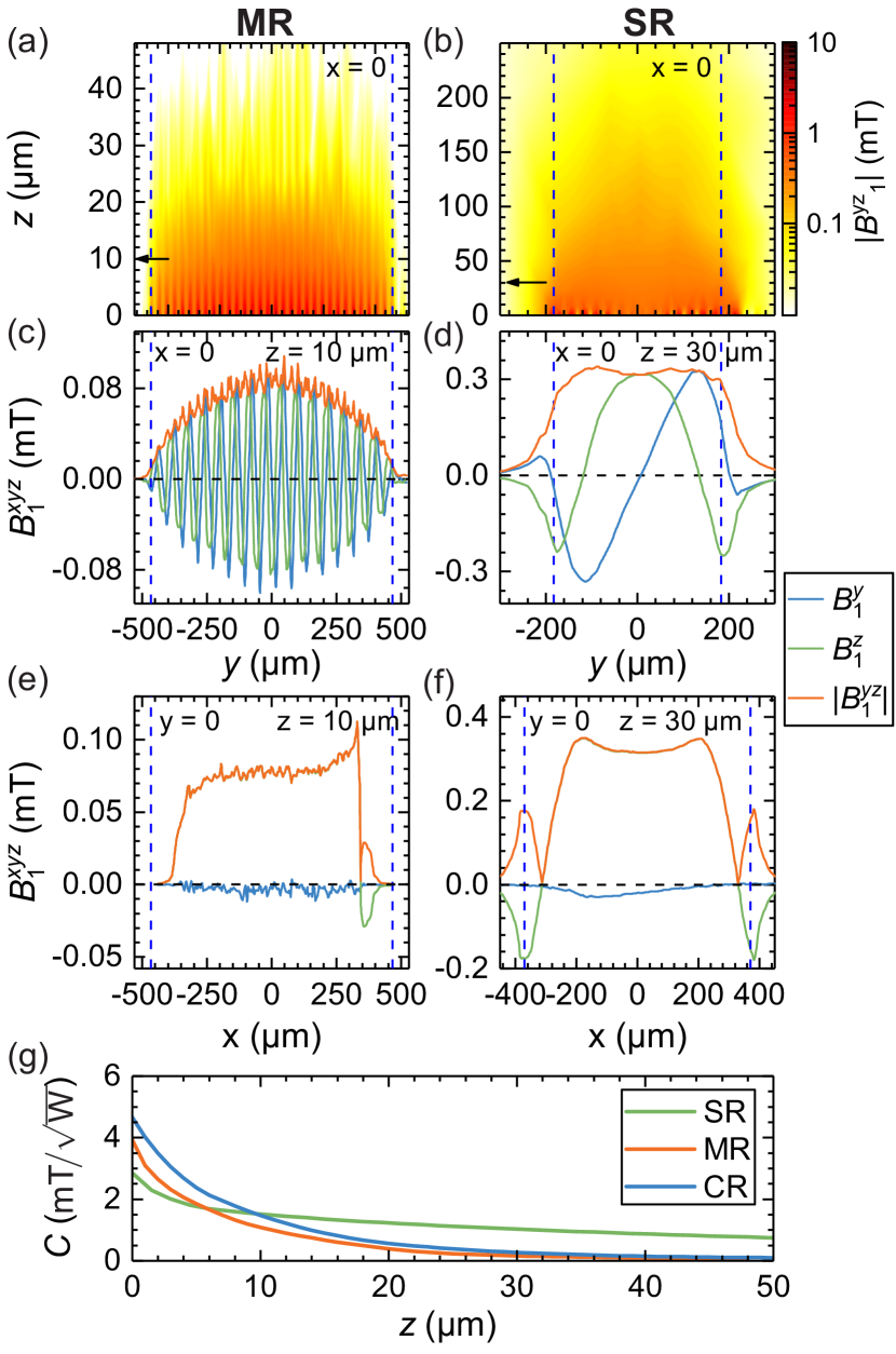
In the MR, the microwave current in adjacent wires flows anti-parallel, resulting in opposing microwave magnetic fields. This is reflected in the homogeneity plot in panel (a) and is also the reason of the fast decay of the magnetic field in the far field. In contrast, the coil-like arrangement of the inductor wire in the SR leads to a parallel current-flow in the two halves of the resonator and therefore to a larger homogeneity. Furthermore, the magnetic field generated by neighboring strips does not cancel in the far field and decays slower than for the MR (note the different scaling of the ordinate). To further highlight the difference between the two designs, we show cuts at a fixed distance above the resonator (arrows in panel (a) and (b)) for and plot the components and as well as the magnitude for the MR and SR along the -axis in Fig. 2 (c) and (d), respectively. The oscillatory behavior of the magnetic field can be clearly seen for the MR, while homogeneous excitation is obtained for the SR. In Fig. 2 (e) and (f), we plot the field components at a fixed distance above the resonator along the -axis. Along this axis, the field homogeneity of the MR is significantly improved.
The MR generates a maximum field of at a distance of , compared to at for the SR. For a more detailed analysis, we evaluate the conversion factor , which is defined asPoole (1996)
| (9) |
where is the resonator quality factor and is the applied microwave power. We assume a sample with -dimensions much larger than the lateral extent of the resonator. is the mean microwave magnetic field in a slice with thickness ( for the SR) with dimensions corresponding to the exported field distribution. The conversion factors for the three resonators are displayed in Fig. 2 (e) as a function of the distance above the resonator. Directly above the resonator, the MR and CR show the highest conversion factors with values up to . This value is more than one order of magnitude larger than that of commercially available resonators. When the distance to the resonator increases, the conversion factor of the MR and CR decreases faster than for the SR. This is due to the large inhomogeneity and the fast decay along the -direction of the MR and CR. Please note that due to the different quality factors of the resonators the conversion factor do not allow a direct comparison of the obtained maximum amplitude.
The simulated three-dimensional field distribution can also be used to estimate the mode volume , to the region where the field amplitude decays to of its maximum value. As can be seen in Table 1, the mode volume of the SR is increased compared to the other designs, in particular in regard to the smaller lateral dimensions.
IV Experimental Details
IV.1 Sample fabrication and measurement setup
To fabricate the sample, we first sputter-deposit a thin layer of Nb with a Al capping layer on a high resistivity () natSi substrate with a thickness of (we do not take the Al capping layer into account in our simulations). The Al capping layer is introduced to prevent oxidation of the Nb layer. The resonators are patterned using a standard electron beam lithography process and subsequently etched using chemical wet etching for the Al as well as reactive ion etching for the Nb layer. The sample chip is then placed into a copper sample holder and connected to two SMA end launch connectors. The sample holder is mounted into a Helium gas-flow cryostat operated at for all of our experiments.
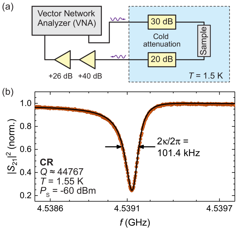
Figure 3 (a) schematically depicts the microwave circuitry of our experiments. For the ESR experiments we apply a external magnetic field parallel to the Nb film plane provided by a superconducting solenoid. We measure the complex microwave transmission amplitude by connecting the sample to the two ports of a vector network analyzer (VNA). Hereby, we can determine the uncalibrated power transmission of the sample. The signal is attenuated by () in the input (output) line inside the cryostat to avoid saturation of the ESR transitions by room temperature thermal microwave photons. The signal is amplified by two room-temperature low-noise amplifiers before detection.
Figure 3 (b) shows an exemplary measurement, where the transmission (points) is plotted against the frequency. The measurement was recorded at zero magnetic field and no sample was mounted on the chip. The attenuators were not present. For the normalization, we set the off-resonant transmission to one. When the excitation frequency is in resonance with the microwave resonator, the transmission drops to about 0.15. In order to extract the resonance frequency, the linewidth, as well as the coupling rate of the microwave resonator to the microwave feedline from the measured complex data, we use a robust circle fit (solid line) described by Probst et al.Probst et al. (2015).
We summarized the relevant parameters for the resonators used in this work in Table 1. The resonance frequency as well as the quality factors are extracted from transmission measurements with a mounted Si:P crystal, as described above. The extraction of the collective coupling rate, its theoretical calculation and the estimation of the Si:P crystal-resonator gap is described in Section IV.4.
| Resonator | Dimensions | ||||||||
|---|---|---|---|---|---|---|---|---|---|
| () | () | (GHz) | (kHz) | (kHz) | () | ||||
| SR | |||||||||
| MR | |||||||||
| CR |
IV.2 Comparison of the resonator parameters: Experiments vs. FEM
To verify our simulation approach, we fabricated two sample chips with several capacitively-shunted resonators (CR). We measure the complex transmission with no external applied magnetic field and extract the resonance frequency as well as the external coupling rate. The measurements were performed without a sample, therefore we have excluded the additional silicon body on top of the resonator in the simulations for this section.
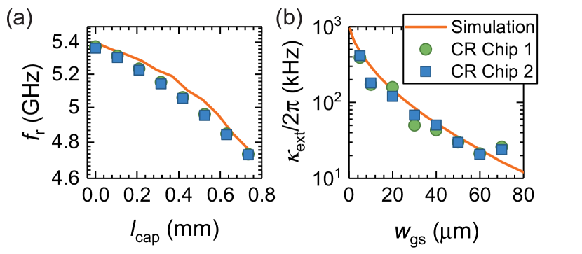
In Fig. 4 (a) we compare the measured and simulated resonance frequency as a function of the length of the capacitor finger . Increasing results in a higher total capacitance and therefore a decrease in the resonance frequency. The simulations (orange line) reproduce the measurement results quantitatively within of the resonance frequency. Nevertheless, the frequency is slightly overestimated, which we attribute to modeling the superconductor as a perfect electric conductor neglecting the effects of superconducting properties. In panel (b), the external coupling rate is plotted as a function of the width of the ground line , separating the resonator window from the CPW (see Fig. 1 (b)). As expected, reducing increases the coupling. The coupling rate roughly shows an exponential behaviour with the separation between the resonator and the feedline. This is due to the screening of the microwave radiation of the feedline by a metallized strip with a width between the two circuit elements. Again, we find excellent qualitative agreement between the experimental data and the finite element modeling.
IV.3 Continuous-wave electron spin resonance
We perform continuous-wave ESR measurements by placing a phosphorus-doped natSi sample with a donor density of in flip-chip geometry on the sample chip. For the following measurements, both attenuators in the cold part of the microwave circuitry are in place.
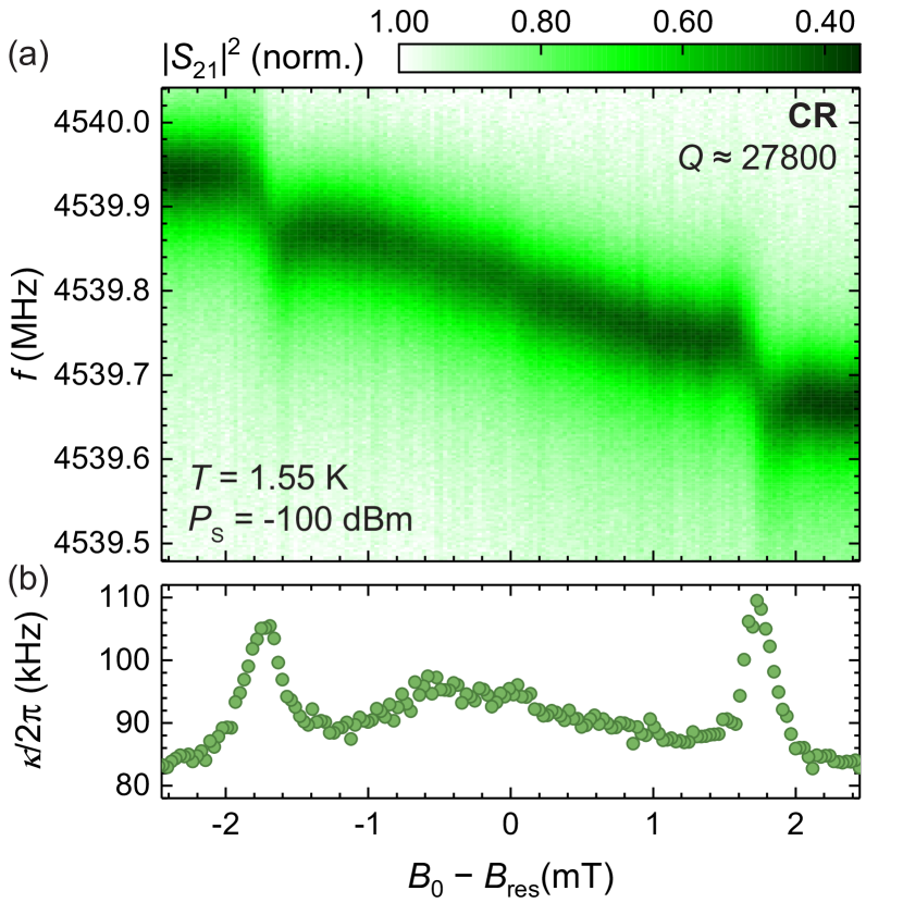
In Fig. 5 (a) we show the normalized transmission as a function of probe frequency and the static applied magnetic field relative to the center resonance field . The transmission is reduced to about 0.35, when the excitation frequency is in resonance with the microwave transmission. We further observe a shift of the resonance frequency over the displayed magnetic field range which we attribute to the magnetic field dependent kinetic inductance of the superconductor. The applied magnetic field leads to an increase in kinetic inductance and hereby also the total inductance of the resonator, changing . Further, we observe two distinct features at , which are identified as the two hyperfine transitions of the phosphorus donors in silicon.
For a more detailed analysis we determine the resonator linewidth as a function of the applied magnetic field. For this, we extract from the transmission spectra for each magnetic field step. This corresponds to a continuous-wave ESR measurement, where the quality factor (absorption signal) of the resonator is measuredPoole (1996). We plot as a function of the applied static field in Fig. 5 (b). In this representation, the two peaks correspond to the two hyperfine transitions analogously. In the magnetic field range between the two peaks we observe additional broad features corresponding to two additional spin systems. The resonance fields of those peaks are compatible with (i) dangling bond defects at the Si/SiO2 interface, known as Pb0/Pb1 defectsPoindexter et al. (1981); Stesmans and Afanas’ev (1998) (), and (ii) exchange-coupled donor pairs forming P2 dimersFeher et al. (1955); Jérome and Winter (1964) ().
Note that we did not perform a field calibration to absolute values. The static magnetic field in our experiments is generated by a large superconducting solenoid, which exhibits a significant amount of trapped flux. This leads to field offsets in the order of . However, in our work the absolute magnetic field applied to the Si:P crystal is only of subordinate interest and we therefore plot the magnetic field relative to the expected center resonance field.
For the applied power of , corresponding to an average photon number of (c.f. Eq. (7)), we observe the onset of saturation effects (see Section IV.5). In order to calculate the collective coupling between the spin ensemble and the microwave resonator in the next section, we choose a dataset, where the microwave power was decreased to ( photons on average). We also point out the importance of the additional attenuators in the setup to suppress thermal microwave noise photons generated at room temperature. Without the attenuation, we observed the onset of saturation effects already at microwave powers as low as .
IV.4 Analysis of the collective coupling
In the following we analyze the collective coupling between the microwave resonator and the high-field hyperfine transition of the phosphorus donors. In Fig. 6 (a) we show the extracted linewidth plotted against the applied static field, relative to the resonance field of the high-field hyperfine transition. The microwave power applied to the sample is to avoid saturation of the ESR transition.
The linewidth in the weak coupling regime can then be described byHerskind et al. (2009)
| (10) |
where is the off-resonant linewidth of the resonator, is the spin linewidth (full-width at half maximum) and is the collective coupling rate. The detuning is defined as . We fit Eq. (10) in combination with a linear background (dashed line) to the data presented in Fig. 6 (a) (solid lines). We extract a collective coupling rate . The resonator linewidth at is . The inhomogeneously broadened spin linewidth (half-width at half maximum) is , corresponding to a linewidth . This is in agreement with literature values for natSi with a natural abundance of 29Si nucleiAbe et al. (2010); Note (1). Note that the lineshape of the ESR transition depends on the residual 29Si concentration in the sampleAbe et al. (2010). For small 29Si concentrations, the lineshape is given by a Lorentzian. However, the transition from Lorentzian to Gaussian lineshape happens at a 29Si concentration of , which is the case for our sample. For our analysis, we therefore performed fits with Gaussian and Lorentzian lineshapes. We only observe a good agreement when fitting a Lorentzian peak, confirming that using Eq. (10) is valid.
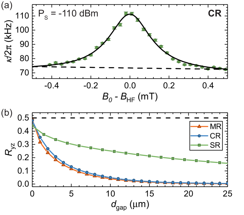
For a first theoretical estimate of , we assume an effective spin density , as only half of the spins contribute to each hyperfine transitionNote (2). The thermal spin polarization at and with the magnetic field on resonance is Zollitsch et al. (2015). With these values we obtain for the CR a collective coupling rate , over-estimating the measured value by more than . This deviation can be explained by a finite gap between the resonator and the Si:P crystal, reducing the effective filling factor.
To analyze the dependence of the effective coupling rate on the finite gap size , we calculate the filling factor for the different designs by taking only for in Eq. (6) into account. We plot as a function of in Fig. 6 (b). We observe a qualitative difference between the CR/MR and the SR. Due to the short decay length of the dynamic magnetic field for the CR and MR, a finite gap shows a significant effect on the coupling strength for these two designs. In contrast, the larger mode volume of the SR leads to a more favorable dependence. Due to the different ratio of components of the dynamic magnetic field perpendicular to the static magnetic field, the maximum value for differs for the three designs. We find a maximum value of for the spiral resonator, for the CR and for the MR.
Using the data presented in Fig. 6 (b), we can estimate the nominal gap between the Si:P crystal and the resonator plane. The measured collective coupling rate of corresponds to a gap of . We performed the same analysis of the collective coupling for the SR and MR and present the extracted parameters in Table 1.
From our simulations, we are able to estimate the number of spins addressed in the measurement using the three-dimensional field distribution and the collective coupling rate from experiment and obtain . Comparing this number to the number of excitations in the resonator using Eq. 7, , confirms that we are in the low-excitation regime. Since , our modelling of the collective coupling is valid, even though the resonator is not in the ground stateChiorescu et al. (2010). It is therefore also applicable at Millikelvin temperatures in the context of ultra-sensitive solid-state ESR.
IV.5 Power saturation
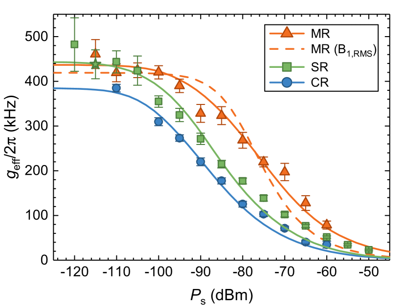
Our theoretical model also allows us to calculate the collective coupling strength as a function of the applied microwave power and to take the effects of power saturation into account. In electron spin resonance, power saturation is a well-known phenomenonCastner (1959); Cullis (1976) which leads to a modulation of the ESR signal as a function of the applied microwave power. As the power level increases, the spin system is driven into saturation. This has also an effect on the collective coupling rate , as it leads to an effective decoupling of the spin system from the microwave resonatorAngerer et al. (2017).
In Fig. 7 we plot the collective coupling rate as a function of the applied power for the three resonator geometries. The collective coupling rates were obtained using the procedure described in the previous section. The SR and MR achieve the highest coupling rates of about . All three curves show a decrease of the collective coupling with increasing power, suggesting a power-dependent saturation effect.
In order to model the power dependence, we take the saturation of the ESR signal into account. In a continuous-wave ESR experiment, the signal increases with the microwave driving field and the signal intensity is therefore given byFajer et al. (1992)
| (11) |
Here, is the gyromagnetic ratio and and are the spin life time and spin coherence time, respectively. The exponent of is valid for an inhomogeneously broadened spin ensemble, which is the case for natSi with abundant 29Si nucleiAbe et al. (2010). is a factor independent of and the factor models the power saturation. For , the denominator in Eq. (11) is equal to one and the spin ensemble is in the unsaturated regime. The correction factor accounts for Lorentzian or Gaussian lineshapes and is determined via a least-squares fitting procedure. For the -field in this equation we use the exported field distribution from our simulation data. We rescale the magnetic field in Eq. (11) according to to obtain a power-dependent expression. Using this result, we can modify Eq. (6) to take power saturation into account and obtain
| (12) |
The solid lines in Fig. 7 are fits of Eq. (12) to the data with the correction factor being the only free parameter. The values of and are extracted from pulsed ESR measurements. We obtain a good agreement of the data with our model if the full field distribution is taken into account. Using only the root-mean square amplitude of the field distribution, we do obtain a significantly worse agreement between theory and experiment (dashed line). The good agreement of our model regarding the power saturation behaviour again confirms our understanding of spatial extent of the microwave excitation field.
V Discussion and conclusion
In this work, we presented three different resonator designs. All designs offer distinct advantages, and therefore choosing the appropriate resonator geometry depends on the intended application. Superconducting planar resonators are used in two different experimental configurations with a different interface between the spin ensemble and the microwave resonator. First, one widely used method is the flip-chip configuration, where the spin sample is placed on top of the resonator, while the resonator itself is placed onto a separate substrate (e.g. Ref. 16; 18; 19; 20 and this work). This type of sample mounting offers greater experimental flexibility, as the sample preparation and placement is independent of the fabrication of the resonator. However, due to the flip-chip geometry, the presence of a small gap between the microwave resonator and the spin sample is highly likely, in particular when working with solid state samples. Another option is to pattern the microwave resonator directly onto a substrate which already contains the spin ensemble (e.g. Ref. 57; 58; 14). Here, the direct interface between the spin ensemble and the microwave resonator offers the largest spin-photon coupling rates but comes with the disadvantage of strain-induced spin resonance shiftsPla et al. (2018). The latter are e.g. caused by different lattice constants and thermal expansion coefficients of substrate and the superconducting thin film material of the resonator.
From our simulation and experimental results, we can draw two conclusions. First, the simulated field distribution of the SR shows that this design is favorable for a homogeneous excitation of the spin ensemble in a flip-chip geometry. The microwave magnetic field decays slowly along the -direction and therefore offers spin excitation throughout the whole spin sample region, even for bulk samples. This makes this design more robust against the presence of a gap between the resonator and the spin sample. For better controlled resonator-to-spin sample distance and an even more enhanced field homogeneity, a thin polyimid (Kapton) spacer can be inserted between the microwave resonator and the spin sample to avoid inhomogeneities in the near-field of the resonatorBenningshof et al. (2013). From the simulations of the SR we find an extended region of thickness with an homogeneity better than , comparable to commercial microwave resonators.
Second, if high single spin coupling rates are desired, a resonator with a meander-shaped strip patterned directly on top of a thin layer containing the spin ensemble offers the best performance. In particular, the CR design with its large finger capacitor and therefore small inductance offers a high current density and therefore a large field, increasing the single spin coupling rateEichler et al. (2017). Additionally, the periodic pattern of the meandering wire allows to engineer microwave antennas that emit microwaves with a specific wavevector. This is a concept that is widely used in spin wave resonance spectroscopy, where excitation at a non-zero wave vector is desirableBailleul et al. (2003).
To summarize, we have analyzed three designs for superconducting planar lumped element resonators. We performed finite element method based simulations to extract the resonance frequency and the quality factor as well as to calculate the characteristic magnetic field distribution of each resonator. We obtained a good agreement between the simulations and the experimental results of fabricated chips, where the resonators were structured into a Nb film. The spiral resonator exploits the two-dimensional coil-like arrangement of the resonator wire to obtain an improved magnetic field homogeneity as well as an increased filling factor when a finite gap between the Si:P crystal and resonator is present. To demonstrate the feasibility of the resonators for magnetic resonance experiments, we presented continuous-wave ESR measurements on phosphorus-doped natSi using all three resonator designs. In order to explain the extracted collective coupling rates, we extended our existing theoretical model to take the simulated microwave magnetic field distribution into account and found a good agreement between the data and the model. Finally, we extracted the collective coupling rate as a function of applied microwave power and modeled the saturation behavior using our model. Our research demonstrates the feasibility of finite element method based simulations to extract the expected collective coupling rate of a spin ensemble coupled to a microwave resonator and gives insight into the different application cases of the resonator designs.
Acknowledgements.
We thank stimulating discussions with S. T. B. Goennenwein and M. S. Brandt. We acknowledge financial support from the German Research Foundation via SPP 1601 (HU 1896/2-1).References
- Poole (1996) Charles P. Poole, Electron Spin Resonance: A Comprehensive Treatise on Experimental Techniques (Dover Publications, Mineola, N.Y, 1996).
- Schweiger and Jeschke (2001) Arthur Schweiger and Gunnar Jeschke, Principles of Pulse Electron Paramagnetic Resonance (Oxford University Press, Oxford, UK ; New York, 2001).
- Narkowicz et al. (2005) R. Narkowicz, D. Suter, and R. Stonies, “Planar microresonators for EPR experiments,” Journal of Magnetic Resonance 175, 275–284 (2005).
- Narkowicz et al. (2008) R. Narkowicz, D. Suter, and I. Niemeyer, “Scaling of sensitivity and efficiency in planar microresonators for electron spin resonance,” Review of Scientific Instruments 79, 084702 (2008).
- Torrezan et al. (2009) A. C. Torrezan, T. P. Mayer Alegre, and G. Medeiros-Ribeiro, “Microstrip resonators for electron paramagnetic resonance experiments,” Review of Scientific Instruments 80, 075111 (2009).
- Malissa et al. (2013) H. Malissa, D. I. Schuster, A. M. Tyryshkin, A. A. Houck, and S. A. Lyon, “Superconducting coplanar waveguide resonators for low temperature pulsed electron spin resonance spectroscopy,” Review of Scientific Instruments 84, 025116 (2013).
- Benningshof et al. (2013) O.W.B. Benningshof, H.R. Mohebbi, I.A.J. Taminiau, G.X. Miao, and D.G. Cory, “Superconducting microstrip resonator for pulsed ESR of thin films,” Journal of Magnetic Resonance 230, 84–87 (2013).
- Sigillito et al. (2014) A. J. Sigillito, H. Malissa, A. M. Tyryshkin, H. Riemann, N. V. Abrosimov, P. Becker, H.-J. Pohl, M. L. W. Thewalt, K. M. Itoh, J. J. L. Morton, A. A. Houck, D. I. Schuster, and S. A. Lyon, “Fast, low-power manipulation of spin ensembles in superconducting microresonators,” Applied Physics Letters 104, 222407 (2014).
- Devoret and Schoelkopf (2013) M. H. Devoret and R. J. Schoelkopf, “Superconducting Circuits for Quantum Information: An Outlook,” Science 339, 1169 (2013).
- Wesenberg et al. (2009) J. H. Wesenberg, A. Ardavan, G. A. D. Briggs, J. J. L. Morton, R. J. Schoelkopf, D. I. Schuster, and K. Mølmer, “Quantum Computing with an Electron Spin Ensemble,” Physical Review Letters 103, 070502 (2009).
- Wu et al. (2010) H. Wu, R. E. George, J. H. Wesenberg, Klaus Mølmer, D. I. Schuster, R. J. Schoelkopf, K. M. Itoh, A. Ardavan, J. J. L. Morton, and G. A. D. Briggs, “Storage of Multiple Coherent Microwave Excitations in an Electron Spin Ensemble,” Physical Review Letters 105, 140503 (2010).
- Abe et al. (2011) Eisuke Abe, Hua Wu, Arzhang Ardavan, and John J. L. Morton, “Electron spin ensemble strongly coupled to a three-dimensional microwave cavity,” Applied Physics Letters 98, 251108 (2011).
- Sandner et al. (2012) K. Sandner, H. Ritsch, R. Amsüss, Ch. Koller, T. Nöbauer, S. Putz, J. Schmiedmayer, and J. Majer, “Strong magnetic coupling of an inhomogeneous nitrogen-vacancy ensemble to a cavity,” Physical Review A 85, 053806 (2012).
- Probst et al. (2017) S. Probst, A. Bienfait, P. Campagne-Ibarcq, J. J. Pla, B. Albanese, J. F. Da Silva Barbosa, T. Schenkel, D. Vion, D. Esteve, K. Mølmer, J. J. L. Morton, R. Heeres, and P. Bertet, “Inductive-detection electron-spin resonance spectroscopy with 65 spins/ Hz sensitivity,” Applied Physics Letters 111, 202604 (2017).
- Bienfait et al. (2017) A. Bienfait, P. Campagne-Ibarcq, A. H. Kiilerich, X. Zhou, S. Probst, J. J. Pla, T. Schenkel, D. Vion, D. Esteve, J. J. L. Morton, K. Moelmer, and P. Bertet, “Magnetic Resonance with Squeezed Microwaves,” Physical Review X 7, 041011 (2017).
- Kubo et al. (2010) Y. Kubo, F. R. Ong, P. Bertet, D. Vion, V. Jacques, D. Zheng, A. Dréau, J.-F. Roch, A. Auffeves, F. Jelezko, J. Wrachtrup, M. F. Barthe, P. Bergonzo, and D. Esteve, “Strong Coupling of a Spin Ensemble to a Superconducting Resonator,” Physical Review Letters 105, 140502 (2010).
- Schuster et al. (2010) D. I. Schuster, A. P. Sears, E. Ginossar, L. DiCarlo, L. Frunzio, J. J. L. Morton, H. Wu, G. A. D. Briggs, B. B. Buckley, D. D. Awschalom, and R. J. Schoelkopf, “High-Cooperativity Coupling of Electron-Spin Ensembles to Superconducting Cavities,” Physical Review Letters 105, 140501 (2010).
- Amsüss et al. (2011) R. Amsüss, Ch. Koller, T. Nöbauer, S. Putz, S. Rotter, K. Sandner, S. Schneider, M. Schramböck, G. Steinhauser, H. Ritsch, J. Schmiedmayer, and J. Majer, “Cavity QED with Magnetically Coupled Collective Spin States,” Physical Review Letters 107, 060502 (2011).
- Probst et al. (2013) S. Probst, H. Rotzinger, S. Wünsch, P. Jung, M. Jerger, M. Siegel, A. V. Ustinov, and P. A. Bushev, “Anisotropic Rare-Earth Spin Ensemble Strongly Coupled to a Superconducting Resonator,” Physical Review Letters 110, 157001 (2013).
- Zollitsch et al. (2015) Christoph W. Zollitsch, Kai Mueller, David P. Franke, Sebastian T. B. Goennenwein, Martin S. Brandt, Rudolf Gross, and Hans Huebl, “High cooperativity coupling between a phosphorus donor spin ensemble and a superconducting microwave resonator,” Applied Physics Letters 107, 142105 (2015).
- Chiorescu et al. (2010) I. Chiorescu, N. Groll, S. Bertaina, T. Mori, and S. Miyashita, “Magnetic strong coupling in a spin-photon system and transition to classical regime,” Physical Review B 82 (2010), 10.1103/PhysRevB.82.024413.
- Wen (1969) C.P. Wen, “Coplanar Waveguide: A Surface Strip Transmission Line Suitable for Nonreciprocal Gyromagnetic Device Applications,” IEEE Transactions on Microwave Theory and Techniques 17, 1087–1090 (1969).
- Lindström et al. (2009) T. Lindström, J. E. Healey, M. S. Colclough, C. M. Muirhead, and A. Ya. Tzalenchuk, “Properties of superconducting planar resonators at millikelvin temperatures,” Physical Review B 80, 132501 (2009).
- Khalil et al. (2011) Moe S. Khalil, F. C. Wellstood, and Kevin D. Osborn, “Loss Dependence on Geometry and Applied Power in Superconducting Coplanar Resonators,” IEEE Transactions on Applied Superconductivity 21, 879–882 (2011).
- Geerlings et al. (2012) K. Geerlings, S. Shankar, E. Edwards, L. Frunzio, R. J. Schoelkopf, and M. H. Devoret, “Improving the quality factor of microwave compact resonators by optimizing their geometrical parameters,” Applied Physics Letters 100, 192601 (2012).
- Wallace and Silsbee (1991) W. J. Wallace and R. H. Silsbee, “Microstrip resonators for electron-spin resonance,” Review of Scientific Instruments 62, 1754–1766 (1991).
- Kupce and Freeman (1995) E. Kupce and R. Freeman, “Adiabatic Pulses for Wideband Inversion and Broadband Decoupling,” Journal of Magnetic Resonance, Series A 115, 273–276 (1995).
- Tannús et al. (1997) Alberto Tannús, Michael Garwood, et al., “Adiabatic pulses,” NMR in Biomedicine 10, 423–434 (1997).
- Garwood and DelaBarre (2001) Michael Garwood and Lance DelaBarre, “The Return of the Frequency Sweep: Designing Adiabatic Pulses for Contemporary NMR,” Journal of Magnetic Resonance 153, 155–177 (2001).
- Skinner et al. (2011) Thomas E. Skinner, Michael Braun, Klaus Woelk, Naum I. Gershenzon, and Steffen J. Glaser, “Design and application of robust rf pulses for toroid cavity NMR spectroscopy,” Journal of Magnetic Resonance 209, 282–290 (2011).
- Spindler et al. (2012) Philipp E. Spindler, Yun Zhang, Burkhard Endeward, Naum Gershernzon, Thomas E. Skinner, Steffen J. Glaser, and Thomas F. Prisner, “Shaped optimal control pulses for increased excitation bandwidth in EPR,” Journal of Magnetic Resonance 218, 49–58 (2012).
- Turneaure et al. (1991) J. P. Turneaure, J. Halbritter, and H. A. Schwettman, “The surface impedance of superconductors and normal conductors: The Mattis-Bardeen theory,” Journal of Superconductivity 4, 341–355 (1991).
- Göppl et al. (2008) M. Göppl, A. Fragner, M. Baur, R. Bianchetti, S. Filipp, J. M. Fink, P. J. Leek, G. Puebla, L. Steffen, and A. Wallraff, “Coplanar waveguide resonators for circuit quantum electrodynamics,” Journal of Applied Physics 104, 113904 (2008).
- Megrant et al. (2012) A. Megrant, C. Neill, R. Barends, B. Chiaro, Yu Chen, L. Feigl, J. Kelly, Erik Lucero, Matteo Mariantoni, P. J. J. O’Malley, D. Sank, A. Vainsencher, J. Wenner, T. C. White, Y. Yin, J. Zhao, C. J. Palmstrøm, John M. Martinis, and A. N. Cleland, “Planar superconducting resonators with internal quality factors above one million,” Applied Physics Letters 100, 113510 (2012).
- Schoelkopf and Girvin (2008) R. J. Schoelkopf and S. M. Girvin, “Wiring up quantum systems,” Nature 451, 664–669 (2008).
- Blais et al. (2004) Alexandre Blais, Ren-Shou Huang, Andreas Wallraff, S. M. Girvin, and R. J. Schoelkopf, “Cavity quantum electrodynamics for superconducting electrical circuits: An architecture for quantum computation,” Physical Review A 69 (2004), 10.1103/PhysRevA.69.062320.
- Grèzes (2015) Cécile Grèzes, TOWARDS A SPIN ENSEMBLE QUANTUM MEMORY FOR SUPERCONDUCTING QUBITS, Ph.D. thesis, CEA Saclay (2015).
- Tosi et al. (2014) Guilherme Tosi, Fahd A. Mohiyaddin, Hans Huebl, and Andrea Morello, “Circuit-quantum electrodynamics with direct magnetic coupling to single-atom spin qubits in isotopically enriched 28 Si,” AIP Advances 4, 087122 (2014).
- Dicke (1954) R. H. Dicke, “Coherence in Spontaneous Radiation Processes,” Physical Review 93, 99–110 (1954).
- Huebl et al. (2013) Hans Huebl, Christoph W. Zollitsch, Johannes Lotze, Fredrik Hocke, Moritz Greifenstein, Achim Marx, Rudolf Gross, and Sebastian T. B. Goennenwein, “High Cooperativity in Coupled Microwave Resonator Ferrimagnetic Insulator Hybrids,” Physical Review Letters 111, 127003 (2013).
- GmbH (2016) CST Computer Simulation Technology GmbH, “CST Microwave Studio 2016,” (2016).
- Mattis and Bardeen (1958) D. C. Mattis and J. Bardeen, “Theory of the Anomalous Skin Effect in Normal and Superconducting Metals,” Physical Review 111, 412–417 (1958).
- Niemczyk et al. (2009) T Niemczyk, F Deppe, M Mariantoni, E P Menzel, E Hoffmann, G Wild, L Eggenstein, A Marx, and R Gross, “Fabrication technology of and symmetry breaking in superconducting quantum circuits,” Superconductor Science and Technology 22, 034009 (2009).
- Probst et al. (2015) S. Probst, F. B. Song, P. A. Bushev, A. V. Ustinov, and M. Weides, “Efficient and robust analysis of complex scattering data under noise in microwave resonators,” Review of Scientific Instruments 86, 024706 (2015).
- Poindexter et al. (1981) Edward H. Poindexter, Philip J. Caplan, Bruce E. Deal, and Reda R. Razouk, “Interface states and electron spin resonance centers in thermally oxidized (111) and (100) silicon wafers,” Journal of Applied Physics 52, 879 (1981).
- Stesmans and Afanas’ev (1998) A. Stesmans and V. V. Afanas’ev, “Electron spin resonance features of interface defects in thermal (100)Si/SiO2,” Journal of Applied Physics 83, 2449 (1998).
- Feher et al. (1955) G. Feher, R. C. Fletcher, and E. A. Gere, “Exchange Effects in Spin Resonance of Impurity Atoms in Silicon,” Physical Review 100, 1784 (1955).
- Jérome and Winter (1964) D. Jérome and J. M. Winter, “Electron Spin Resonance on Interacting Donors in Silicon,” Physical Review 134, A1001 (1964).
- Herskind et al. (2009) Peter F. Herskind, Aurélien Dantan, Joan P. Marler, Magnus Albert, and Michael Drewsen, “Realization of collective strong coupling with ion Coulomb crystals in an optical cavity,” Nature Physics 5, 494 (2009).
- Abe et al. (2010) Eisuke Abe, Alexei M. Tyryshkin, Shinichi Tojo, John J. L. Morton, Wayne M. Witzel, Akira Fujimoto, Joel W. Ager, Eugene E. Haller, Junichi Isoya, Stephen A. Lyon, Mike L. W. Thewalt, and Kohei M. Itoh, “Electron spin coherence of phosphorus donors in silicon: Effect of environmental nuclei,” Physical Review B 82, 121201 (2010).
- Note (1) We estimate the contribution to the inhomogeneous broadening due to an inhomogeneous field to be less than , based on the specified field homogeneity of the solenoid. Due to the way the Si:P crystal is mounted on the resonator, the influence of strain on the inhomogeneous broadening is negligible.
- Note (2) In our calculation we use the nominal donor concentration as the density, assuming that each donor contributes equally to the collective coupling. However, for donor concentrations , phosphorus dimers and trimers are formed, which also contribute the the broad background signal and the P2 dimer transition. We therefore calculate the theoretically upper bound of the collective coupling.
- Castner (1959) T. G. Castner, “Saturation of the Paramagnetic Resonance of a V Center,” Physical Review 115, 1506–1515 (1959).
- Cullis (1976) P. R. Cullis, “Electron paramagnetic resonance in inhomogeneously broadened systems: A spin temperature approach,” Journal of Magnetic Resonance (1969) 21, 397–418 (1976).
- Angerer et al. (2017) Andreas Angerer, Stefan Putz, Dmitry O. Krimer, Thomas Astner, Matthias Zens, Ralph Glattauer, Kirill Streltsov, William J. Munro, Kae Nemoto, Stefan Rotter, Jörg Schmiedmayer, and Johannes Majer, “Ultralong relaxation times in bistable hybrid quantum systems,” Science Advances 3, e1701626 (2017).
- Fajer et al. (1992) P. Fajer, A. Watts, and D. Marsh, “Saturation transfer, continuous wave saturation, and saturation recovery electron spin resonance studies of chain-spin labeled phosphatidylcholines in the low temperature phases of dipalmitoyl phosphatidylcholine bilayers. Effects of rotational dynamics and spin-spin interactions,” Biophysical Journal 61, 879–891 (1992).
- Bienfait et al. (2016) A. Bienfait, J. J. Pla, Y. Kubo, M. Stern, X. Zhou, C. C. Lo, C. D. Weis, T. Schenkel, M. L. W. Thewalt, D. Vion, D. Esteve, B. Julsgaard, K. Mølmer, J. J. L. Morton, and P. Bertet, “Reaching the quantum limit of sensitivity in electron spin resonance,” Nature Nanotechnology 11, 253 (2016).
- Eichler et al. (2017) C. Eichler, A. J. Sigillito, S. A. Lyon, and J. R. Petta, “Electron Spin Resonance at the Level of Spins Using Low Impedance Superconducting Resonators,” Physical Review Letters 118, 037701 (2017).
- Pla et al. (2018) J. J. Pla, A. Bienfait, G. Pica, J. Mansir, F. A. Mohiyaddin, Z. Zeng, Y. M. Niquet, A. Morello, T. Schenkel, J. J. L. Morton, and P. Bertet, “Strain-Induced Spin-Resonance Shifts in Silicon Devices,” Physical Review Applied 9, 044014 (2018).
- Bailleul et al. (2003) Matthieu Bailleul, Dominik Olligs, and Claude Fermon, “Propagating spin wave spectroscopy in a permalloy film: A quantitative analysis,” Applied Physics Letters 83, 972–974 (2003).
Appendix A Collective coupling in an inhomogeneous magnetic field
In the following we derive an expression allowing us to calculate the collective coupling rate for a spatially inhomogeneous distribution of the dynamic magnetic field. We first start with the case of a homogeneous field.
The collective coupling strength of a spin ensemble of spins is given bySandner et al. (2012) , where is the single-spin coupling strength of an individual spin in the ensemble. In the case of homogeneous coupling, this expression reduces to with the single-spin coupling rate given byWesenberg et al. (2009)
| (13) |
Here, the coupling strength is determined by the magnetic component of the microwave vacuum field, . This field can be estimated by integrating the energy stored in the magnetic field created by vacuum fluctuations, according toSchoelkopf and Girvin (2008)
| (14) |
The additional factor of in the denominator on the left side of the equation takes into account that half of the energy is stored in the electric component of the vacuum field. Using Eq. (13)) and (14) the collective coupling strength for a spatially homogeneous field distribution is given by
| (15) |
where we have substituted with the effective spin density and the spin sample volume . The ratio is called filling factor and defines the volume of the resonator field filled with the spin ensemble.
In the case of planar resonators, the assumption of a spatially homogeneous field is not valid. Here, we have to take into account the spatial dependence of in Eq. (14). Another point to consider is the orientation of the field with respect to the static magnetic field . In our experiments the static field is applied in-plane along the -axis (c.f. Fig. 1). Only field components perpendicular to can excite spins in the spin ensemble. From our simulations we export the three-dimensional magnetic field , discretized in finite elements with volume . Assuming the field is homogeneous over the spatial extent of a single volume element we find for the collective coupling strength of a single volume element
| (16) |
where is the exported field amplitude of the volume element and is the number of spins in the volume element. The calibration factor rescales the field amplitude from the simulated excitation level to the level of vacuum fluctuations. It can be calculated similar to Eq. (14) by
| (17) |
Note that here we also take the -component of the field into account. We convert the integration into a summation over all volume elements and find for the calibration factor
| (18) |
Combining Eq. (16) and (18) and summing over all volume elements we finally obtain an expression for the collective coupling strength of a spin ensemble coupled to an inhomogeneous microwave magnetic field:
| (19) |
Note that in this expression the size of the volume element effectively cancels out. The last square-root term plays a similar role to the filling factor introduced in Eq. (15).