figuret
Probing alloy formation using different excitonic species:
The particular case of InGaN
Abstract
Since the early 1960s, alloys are commonly grouped into two classes, featuring bound states in the bandgap (I) or additional, non-discrete, band states (II). As a consequence, one can observe either a rich and informative zoo of excitons bound to isoelectronic impurities (I), or the typical bandedge emission of a semiconductor that shifts and broadens with rising isoelectronic doping concentration (II). Microscopic material parameters for class I alloys can directly be extracted from photoluminescence (PL) spectra, whereas any conclusions drawn for class II alloys usually remain indirect and limited to macroscopic assertions. Nonetheless, here, we present a comprehensive spectroscopic study on exciton localization in a so-called mixed crystal alloy (class II) that allows us to access microscopic alloy parameters. In order to exemplify our experimental approach we study bulk InxGa1-xN epilayers at the onset of alloy formation (0 2.4%) in order to understand the material’s particular robustness to point and structural defects. Based on an in-depth PL analysis it is demonstrated how different excitonic complexes (free, bound, and complex bound excitons) can serve as a probe to monitor the dilute limit of class II alloys. From an -dependent linewidth analysis we extract the length scales at which excitons become increasingly localized, meaning that they convert from a free to a bound particle upon alloy formation. Already at the average exciton diffusion length is reduced to at a temperature of 12 K, thus, detrimental exciton transfer mechanisms towards non-radiative defects are suppressed. In addition, the associated low temperature luminescence data suggests that a single indium atom does not suffice in order to permanently capture an exciton. The low density of silicon impurities in our samples even allows studying their local, indium-enriched environment at the length scale of the exciton Bohr radius based on impurity bound excitons. The associated temperature-dependent PL data reveals an alloying dependence for the exciton-phonon coupling. Thus, the formation of the random alloy can not only directly be monitored by the emission of various excitonic complexes, but also more indirectly via the associated coupling(s) to the phonon bath. Micro-PL spectra even give access to a forthright probing of silicon bound excitons embedded in a particular environment of indium atoms, thanks to the emergence of a hierarchy of individual, energetically sharp emission lines (full width at half maximum 300 eV). Consequently, the present spectroscopic study allows us to extract first microscopic alloy properties formerly only accessible for class I alloys.
I Introduction
Upon alloying, host atoms in insulators, semiconductors, or metals are replaced by atoms with an equivalent valence electron structure, giving rise to isoelectronic impurities. Despite the matching valency, which does not lead to - or -type doping in case of a semiconductor crystal, the total number of electrons is altered, inducing fundamental changes in the electronic band structure and the associated optical signatures of alloying Czaja (1971). Already in 1966, Thomas pointed out Thomas (1966) that such isoelectronic impurities can be divided into two classes: For the first class (I), discrete electronic levels are formed in the bandgap that can be studied by the related emission of bound excitons in, e.g., GaP:N Thomas et al. (1965); Zhang et al. (2000), GaP:Bi Faulkner and Dean (1970); Francoeur et al. (2008), GaAs:N Wolford (1979), ZnTe:O Merz (1968), CdS:Te Fukushima and Shionoya (1976), and ZnO:Hg Cullen et al. (2013). However, such highly localized bound excitons caused by isoelectronic centers strongly differ from the wide range of bound excitons known for shallow impurities in semiconductors and cannot be described by an effective mass approach Faulkner (1968); Phillips (1969); Allen (1971). The second class of isoelectronic centers (II) evokes the formation of mixed crystal alloys like, e.g., SiGe Braunstein et al. (1958), GaAsP Tietjen and Weisberg (1965), InGaAs Laurenti et al. (1988), AlGaAs Schubert et al. (1984), InGaN Butté et al. (2018), AlGaN Wagener et al. (2004), CdSSe Goede et al. (1978); Klochikhin et al. (1999), ZnSeTe Klochikhin et al. (1999), and MgZnO Grundmann and Dietrich (2009). In these cases, no new electronic levels are formed in the bandgap, but rather in the bands themselves, a process often described as hybridization Bellaiche et al. (1999). Clearly, such a simple classification is not always straightforward Dean (1970) and even a continuous, concentration-dependent transition between these two classes of isoelectronic centers has been reported for the unique case of silver halides Kanzaki and Sakuragi (1969).
The consequences regarding the existence of these two types of isoelectronic centers in nature for any optical material characterization are pivotal: For class I alloys the apparent rich optical signature Hopfield et al. (1966) allows to directly extract microscopic material parameters from macroscopic photoluminescence (PL) spectra. Not only the number of isoelectronic impurities per binding center can be extracted Francoeur et al. (2008), but even the distance in between these impurities or their constellation can be determined Thomas and Hopfield (1966); Zhang et al. (2000); Muller et al. (2006). In contrast, for class II alloys, the spectroscopic analysis is hampered. Commonly, only a continuous shift of the bandedge luminescence is observable, which is additionally plagued by pronounced linewidth broadening Schubert et al. (1984); Laurenti et al. (1988), preventing any detailed information to be extracted from PL spectra. Consequently, in contrast to class I alloys, only a rather indirect analysis of such mixed crystal alloys is feasible by optical techniques. What further worsens the situation is the fact that isoelectronic impurities related to class II are more abundant in nature in comparison to their type I counterparts Czaja (1971). Furthermore, most technologically relevant alloys (e.g., InGaAs, AlGaAs Manfra (2014), AlInGaP Stringfellow and Craford (1998), InGaN, InAlN Chichibu et al. (2006a), and AlGaN Kneissl et al. (2011)) belong to class II. Here, especially III-nitride alloys have recently proven their importance for a wide range of applications, rendering a spectroscopic analysis beyond the limits of their classification as mixed crystal alloys an auspicious task.
Over the past decade, III-nitride-based semiconductors have reached a high level of dissemination only second to silicon based on a wide range of applications covering both, electronics and optoelectronics Gil (2014). Many aspects of our daily life are already impacted by III-nitride-based light-emitting and laser diodes (LEDs and LDs) Nakamura et al. (1991, 1997), while high-power electronics is also on the rise Mishra et al. (2008); Rajan and Jena (2013). Here, ternary alloys like InGaN and InAlN play a crucial role, as essential properties like, e.g., their emission wavelength can be tuned over wide ranges Wächter et al. (2011) in order to suit the particular application of choice. Such alloys containing indium are often described as ”special alloys”, because many devices like LEDs based on InGaN/GaN quantum wells (QWs) perform astonishingly well, with internal quantum efficiencies well beyond 80% Nippert et al. (2016), even though the threading dislocation density is high with values in the range Ponce and Bour (1997). Generally, the material proves particularly robust against structural and point defects in comparison to other III-V alloys (e.g. InGaAs, AlGaAs, AlInGaP, etc.) Stringfellow and Craford (1998) as outlined in the seminal paper of Chichibu et al. Chichibu et al. (2006a). However, the physical origin behind this behavior is not well understood yet and several possible causes have been discussed in the literature.
Early explanations accounting for the particular case of InGaN range from large structural defects like V-pits Hangleiter et al. (2005) and indium clusters Narukawa et al. (1997), over indium-zig-zag chains Kent and Zunger (2001); Chichibu et al. (2006a), to the particular electronic environment of a single indium atom Bellaiche et al. (1999). All explanations share the common idea that localization of carriers occurs in the alloy, ultimately leading to higher values. As soon as carriers are localized, their diffusion to non-radiative centers is suppressed, which in turn enhances . While larger structural defects can nowadays be excluded for modern III-nitride materials based on a combination of structural [scanning transmission electron microscopy, nanoscale secondary ion mass spectroscopy, etc.] and optical [cathodoluminescence (CL), micro-photoluminescence (-PL), etc.] techniques, the material analysis at the few to even sub-nanometer scale remains challenging. Even though recent technical progress made by atom probe tomography (APT) indicates that InGaN is a random alloy Galtrey et al. (2007); Cerezo et al. (2007); Rigutti et al. (2018), the impact of assemblies of indium atoms like pairs, triplets, and larger sets on the material’s optical signature remains unclear.
In this work, we show that even for class II alloys it is possible to extract microscopic material parameters from PL and -PL spectra. A detailed PL analysis of bulk InxGa1-xN epilayers (0 2.4%) grown on freestanding (FS) GaN substrates (dislocation density ) allows us to extract the effective exciton diffusion length () and its dependence on indium content (). By analyzing the linewidth broadening of free and bound excitons, one obtains probes that monitor the alloy formation on different length scales determined by and the exciton Bohr radius , hence, in our case encompassing length scales ranging from tens to a few nanometers. With rising we measure a decrease of towards using the free exciton () as a probe for the formation of a random alloy in which the excitonic center of mass (COM) movement becomes increasingly negligible at cryogenic temperatures. In addition, the exciton-phonon coupling is studied, e.g., for silicon-bound excitons (), representing an alternative tool to monitor the onset of alloy formation. The spectroscopy of excitons captured at individual indium-related centers proves challenging due to an apparent high density of emitters. Hence, we focus on an analysis of -PL spectra of individual silicon-bound excitons embedded in particular configurations of indium atoms in their direct vicinity. As a result, we observe a hierarchy of energetically well-defined emission lines [full width at half maximum (FWHM) 300 eV] that originate from complexes in the InGaN alloy. Hence, our study opens a pathway towards a spectroscopic analysis of the microscopic properties of a class II alloy at the nanometer scale by probing distinct configurations of indium atoms at the onset of alloy formation.
The paper is structured as follows: In Sec. II we first compare the fundamental excitonic properties of a wide range of materials, before focusing the motivation to III-V semiconductors represented by indium doped GaAs and GaN as representatives of class II alloys. We present our results in Sec. III. This section is subdivided into four parts labeled Secs. III.1-III.4. In Sec. III.1 we show how ensembles of free and bound excitons can serve as probes in the InGaN alloy using PL spectra. Temperature-dependent PL data allows us to analyze the local distribution of indium atoms around particular impurity bound excitons as demonstrated in Sec. III.2. Subsequently, Sec. III.3 introduces the -PL traces of individual excitonic complexes bearing on an impurity embedded in a distinct environment of indium atoms. The spectra of such individual bound excitonic complexes are further analyzed in Sec. III.4, motivating the existence of spatially direct and indirect excitonic complexes in the InGaN alloy. In a nutshell, Secs. III.1-III.4 describe the following transition: first, ensembles of excitonic complexes are probed in the alloy by PL. Second, the presented alloy probes become increasingly localized, culminating in the -PL observation of individual impurity bound excitonic complexes embedded in a distinct configuration of indium atoms. Sec. IV finally relates our PL and -PL results before Sec. V summarizes all findings. Experimental details regarding the spectroscopic and growth techniques can be found in the Supplementary Information (SI) in Sec. I.
II Context and motivation
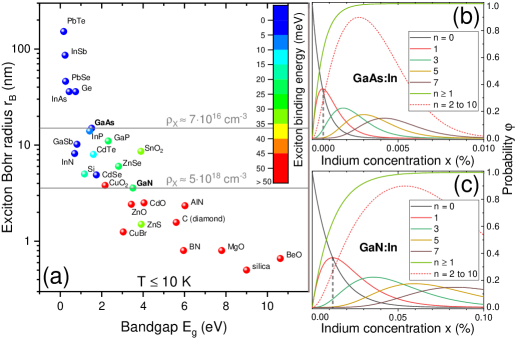
In order to obtain a general understanding of the sensitivity of excitons in alloys to crystal defects, Fig. 1(a) introduces the reduction of (excitonic ground state) with rising bandgap energy for a large variety of materials (direct as well as indirect semiconductors and insulators). The higher the ionicity of the crystal - following the transition from IV-IV, over III-V, to II-VI semiconductors - the larger are the effective masses of the electrons () and holes () that move in the periodic potential of the lattice. In turn, the excitonic effective mass increases accordingly with like , which is inversely proportional to Mathieu et al. (1992). Such ”heavy” excitons with small values ultimately lead to the transition from Wannier-Mott type excitons found in most semiconductors to self-trapped excitons frequently observed in silica Kalceff and Phillips (1995) and halides Tanimura and Itoh (1981). As soon as is reduced, the exciton binding energy rises as the Coulomb attraction between the electron and the hole is enhanced. Hence, is proportional to as encoded in the data-point colors of Fig. 1(a), leading to the experimental stability and the herewith interconnected accessibility of excitons beyond just cryogenic temperatures for large bandgap materials like, e.g., GaN Viswanath et al. (1998) and AlN Onuma et al. (2009).
Already these basic considerations facilitate some conclusions that should be valid for any alloy of class I or II formed by the materials summarized in Fig. 1(a). In alloys with low values an exciton averages at least over comparably large exciton volumes . Hence, correspondingly low densities of, e.g., impurities and structural defects suffice in order to affect or even trap an exciton if the associated perturbation is sufficiently large. In this sense, represents a tentative upper limit for the concentration of such centers affecting all excitons. In contrast, high materials with lower values should be less sensitive to higher defect concentrations based on this simplistic comparison. In order to illustrate this matter, we highlight the corresponding values for GaAs and GaN in Fig. 1(a), providing a first sensitivity estimate for excitons occurring in related alloys. As the value of both materials varies by a factor of , the corresponding approximations of differ by almost two orders of magnitude. However, this comparison is complicated by the occurrence of free, bound (isovalent), and impurity bound (non-isovalent) excitons constituting two- or three-particle complexes. One can either observe free excitons that move and hence monitor the alloy over an averaging volume leading to lower critical values, or localized, shallow impurity bound excitons sensing the material within (see Sec. III.1 for a detailed analysis). Nevertheless, the lower for large materials, the less excitons average over a random alloy and the more they just monitor the immediate neighborhood of a distribution of, e.g., (non-) isovalent centers in the lattice. This simple picture is further supported by the common neglect of any COM movement for excitons in an alloy Zimmermann (1990) - a simplification that will be discussed in detail in Sec. III.1 for InGaN.
We further motivate the present study by focussing our previous considerations to indium-doped GaAs:In (e.g. Ref. (16)) and GaN:In (this work) as representatives for the extremal cases of relatively low and high values in III-V semiconductor alloys of class II. Based on this choice, the associated values would always remain sufficiently high to ensure a straightforward PL analysis. The reasoning that further motivates this approach is threefold:
A) High quality material is available for InGaN and InGaAs alloys for studying the onset of alloy formation for class II alloys due to the availability of high quality substrates for the epitaxial growth of thick, ternary layers () as required for spectroscopy.
B) It is known that InGaAs- and AlGaAs-based LEDs are rather sensitive to the density of point and structural defects, whereas InGaN proves to be much more robust Stringfellow and Craford (1998); Chichibu et al. (2006a) against them.
C) It was pointed out theoretically that individual indium atoms in GaAs and GaN do not lead to any bound states in the bandgap Bellaiche et al. (1999), a matter that would rather require several indium atoms to form larger indium configurations Kent and Zunger (2001).
In other words, both materials are unambiguous representatives of class II alloys with relatively simple spectra that facilitate a detailed tracking of the alloy formation. For class I alloys known bound states are mostly associated to single atoms or (extended) pairs and can be observed for a wide range of materials as summarized in Sec. I. The absence of such optical signatures will allow us to study the very onset of alloy formation in InxGa1-xN (0 2.4%) by monitoring the undisturbed averaging process over the random alloy from the perspective of either free, bound, or impurity-(complex)-bound excitons.
Generally, the probability to find indium atoms in for a certain indium concentration is given by the Bernoulli distribution in a random alloy:
| (1) |
Here, is the cation number in the excitonic volume with 0.0438 Å-3 for wurtzite GaN in the indium composition range analyzed in this paper Vurgaftman and Meyer (2003); Butté et al. (2018). An illustration for the probability to find, e.g., indium atoms in is given for GaN and GaAs ( 0.0221 Å-3) Schubert et al. (1984) in Figs. 1(b) and 1(c), respectively. The indium concentration for which one can find, e.g., one indium atom in with deviates by more than one order of magnitude, due to the about 4 larger value of GaAs in comparison to GaN. This fact will be crucial for the following PL linewidths analysis of the InGaN alloy, providing insight into the material’s particular robustness against point and structural defects Chichibu et al. (2006a).
III Results
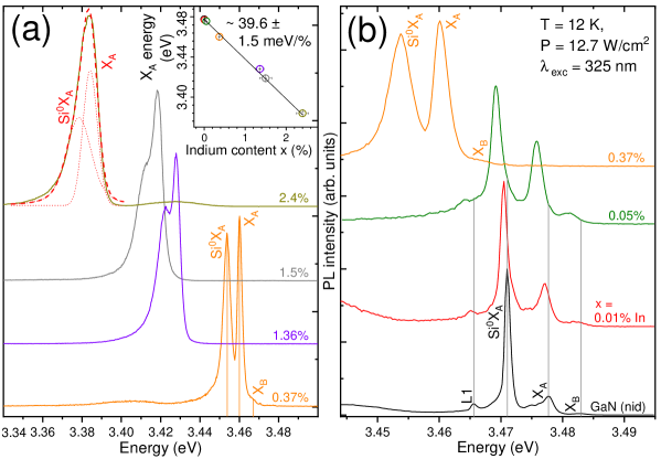
Figure 2 introduces the low temperature (12 K) PL spectra of the bulk InxGa1-xN sample series at hand with an indium content ranging from 0 to 2.4% (see Sec. I in the SI for experimental details). The spectrum of the non-intentionally doped (nid) GaN reference sample shows the common optical traces of the A- and B-exciton ( and ) along with a dominant neutral donor bound exciton line (). The energetic splitting in between and is known as the localization energy Callsen et al. (2018). Generally, this terminology is not only used for excitons binding to non-isovalent impurities, but also for the localization of excitons in an alloy due to isoelectronic impurities that induce the formation of a potential landscape Chichibu et al. (2006a). In both cases, the emission energy of the excitons exhibits a redshift with respect to , which will always be described by in the following. Previous results have shown that the dominant impurity giving rise to the main bound excitonic emission is the neutral silicon center , while other typical trace impurities in GaN like oxygen are negligible in our samples Callsen et al. (2018). In addition, towards lower energies one observes the L1 emission line in Fig. 2(b), whose origin is still under debate in the literature, ranging from a deep, over an ionized donor-bound exciton, to a neutral, shallow acceptor bound exciton Šantic et al. (1997); Monemar et al. (2001); Wysmołek et al. (2003); Fischer et al. (1997).
Upon increasing indium content, the entire set of emission lines shifts continuously towards lower energies, while the level of detail in the spectra diminishes due to linewidth broadening as commonly observed for a class II alloy. The spectral shift of the transition as a function of the change in bandgap energy with rising is linear in the given indium concentration range and amounts to at a temperature of 12 K as shown in the inset of Fig. 2(a). Clear evidence for the emission line L1 is lost at indium concentrations exceeding 0.05%, before even the spectral separation between and vanishes. Nevertheless, even at indium concentrations of 1.5% and 2.4% we can still reveal the presence of the centers in the corresponding spectra by a simple lineshape fitting procedure employing two Voigt profiles as exemplified for in Fig. 2(a). We find the Voigt profiles to be dominated by their Gaussian contribution due to the comparable small influence of homogeneous broadening at a temperature of 12 K. Note that the Voigt profiles from Fig. 2(a) only have an illustrative purpose, highlighting the two different spectral components. In the following all reported FWHM values originate from a manual data reading in order to avoid a troublesome and overparametrized lineshape fitting. We will subsequently analyze the temperature dependence of the linewidths in the context of Fig. 4 in Sec. III.2.
At first glance, the present alloying series of GaN:In seems to match the case of GaAs:In as presented by Laurenti et al. Laurenti et al. (1988) for indium concentrations down to 0.03% in GaAs. A continuous shift and a continuous broadening of all optical transitions are observed in GaN:In down to as expected for a class II alloy. Not even at the very onset of the alloying range one can observe any additional emission lines related to excitons bound to single isoelectronic indium centers in agreement with the aforementioned theoretical predictions Bellaiche et al. (1999). Note that an indium concentration of yields a probability of for a single indium atom to be present in the excitonic volume as shown in Fig. 1(c). Hence, the indium concentration should be sufficiently low to observe the occurrence of any additional bound states induced by single indium atoms.
However, a more detailed inspection of PL and -PL spectra will result in a manifold of interesting and so far unforeseen observations for the InGaN alloy as shown in Secs. III.1-III.4. The latter mark the transition from an analysis dealing with ensembles of excitons down to individual ones giving access to the microscopic properties of a class II alloy.
III.1 Probing alloying with free and bound excitons based on macro-photoluminescence
An in-depth analysis of the emission linewidth of and reveals an intriguing feature for GaN:In that is fostered by its large values and, in comparison to GaAs:In, its smaller values. At a temperature of 12 K and the transition exhibits a FWHM value of while the FWHM of is larger with due to the distribution of free excitons in momentum () space. Interestingly, with rising indium content this FWHM ratio is reversed as seen, e.g., in the PL spectrum recorded for , cf. Fig. 2(b). At this indium concentration we find , while has more than tripled to 4.47 0.08 meV.
The evolution of the experimentally determined values for the and excitonic complexes is summarized in Fig. 3(a) (black and red symbols). Both sets of FWHM values show a different evolution as averaging over the alloy occurs for different effective volumes. All values are commonly related to the peak width by . Generally, such values are composed of an inhomogeneous component due to alloy broadening, , and a homogeneous, temperature-dependent component , caused by phonon scattering, leading in first approximation to Grundmann and Dietrich (2009); Claus Klingshirn (2005). At low temperatures (12 K) dominates any phononic effects giving rise to the experimental trends shown in Fig. 3(a) for the directly measured values. Additional broadening by will subsequently be discussed for in Sec. III.2 in the context of Fig. 4, while the corresponding analysis for is given in SI Sec. III. Such predominance of inhomogeneous broadening due to alloy disorder at cryogenic temperatures was also observed for other ternary alloys of class II such as MgZnO Grundmann and Dietrich (2009), AlGaAs Schubert et al. (1984), CdZnTe Neu et al. (1984), and CdSSe Goede et al. (1978).
Based on Eq. 1, the standard deviation of the bandgap energy can be expressed by the binomial distribution Goede et al. (1978); Schubert et al. (1984):
| (2) |
Hence, for a two-particle system like , should equal the peak width determined via , while is deduced from Fig. 2(a). As a first approach, can be replaced by the standard spherical exciton volume () - a method that commonly yields a good agreement with experimental data Grundmann and Dietrich (2009). However, the quantum mechanical nature of the exciton is completely neglected by this approach, as one assumes a constant occupation probability density for the exciton over . Instead, the quantum-mechanical (qm) exciton volume should rather be considered in order to take the wavefunction of the exciton into account as outlined in Refs. (20) and (52).
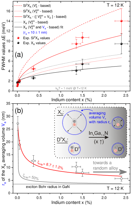
Figure 3(a) shows that both volumes ( and ) either lead to a complete over- (dashed red line) or underestimation (dotted red line) of the experimentally observed trend for as the effect of the donor electron in this three-particle complex is not yet considered. The complex as well as the donor electron sense the alloy formation, leading to energy fluctuations that are normally distributed. Hence, the square of the entire peak width of amounts to: . Here, one obtains based on Ref. (60) with the donor Bohr radius that is derived from the silicon donor binding energy of 28.5 meV Callsen et al. (2018) calculated within the framework of the hydrogenic model Gil et al. (2007). This consideration of as a three-particle complex leads to a reasonable agreement between experiment and theory [Fig. 3(a), solid red line].
In contrast, for the two-particle complex the consideration of (dotted black line) still yields an overestimation for most of the experimentally observed values as the COM movement of the exciton would need to be considered at the onset of the alloy formation. However, even the sophisticated theoretical treatment for alloys of Zimmermann given in Ref. (52) deems the COM movement of the exciton a task for future work, which has - to the best of our knowledge - never been accomplished. As a direct consequence of the excitons’ COM motion, the entire set of complexes averages over a larger fraction of the alloy, hence, we suggest to consider an effective, spherical averaging volume with scaling parameter as a measure for the COM movement. A fit to the experimental data from Fig. 3(a) for yields (solid black line), while the offset between experimental data points and the fit increases with . This indicates that scales with as described in the following.
For , Eq. 2 can be solved for using , yielding the indium content dependent averaging radius of the corresponding volume as shown in Fig. 3(b) (black circles). The value of is continuously decreasing with rising indium content as complexes get increasingly localized by indium-related trapping sites. Ultimately, approaches as the free exciton transforms into a bound two-particle complex as shown in Fig. 3(b) and illustrated in the corresponding inset. In contrast, a complex like always remains a bound complex at the onset of alloy formation and should, as a first approximation, maintain a constant averaging volume. At the present onset of alloy formation, we do not expect any strong influence of on , which is taken in Fig. 3(b) as that of pure GaN. Singlets, doublets, and with rising even more extended complexes of indium atoms [see Fig. 1(c)] should lead to such increasing localization of with rising . In this respect, the reported values represent a measure of the diffusion length. According to Bellaiche et al. Bellaiche et al. (1999) the hole as a building block of the complex can get localized even in the case of a single indium atom. However, the corresponding energy level is still hybridized with the valence band states of GaN, meaning that no additional states appear in the bandgap at the onset of alloy formation in agreement with our observations from Fig. 2 (no new emission lines appear with rising ) and our expectations for a class II alloy. This particular case is fundamentally different from that of conventional excitons bound to isoelectronic centers (cf. examples given in Sec. II) mostly situated on anionic lattice sites Hopfield et al. (1966), whose strong localization leads to the appearance of new energy levels in the bandgap.
Based on a simple, static approximation, the probability to capture at such indium-related sites can be approximated by with the average distance in between the indium atoms in the dilute alloy . This approximation relies on the common assumption made for most III-V Callsen et al. (2012) and II-VI Wagner et al. (2011) semiconductors that the exciton capture time is short compared to the radiative decay time, . Consequently, based on the spherical averaging volume one straightforwardly finds the following relation to fit the data from Fig. 3(b): . Clearly, only for it is possible to obtain a reasonable fit to the experimental data as shown in Fig. 3(b) by the solid red line. Hence, indeed on average a single indium atom per does not seem to provide a sufficiently deep potential in order to permanently capture the complex at the given temperature Bellaiche et al. (1999). This observation represents the main result of the present simple fitting model. For instance, already for the values for would rapidly diminish with rising . This evolution is shown in Fig. 3(b) (solid grey line) and constitutes the reason behind the common neglect of the excitons’ COM movement in alloys Zimmermann (1990), which is not highly diluted, or in other words, just doped.
The fit from Fig. 3(b) yields (solid red line), suggesting that indium-related complexes comprising 10 indium atoms predominantly contribute to the capture of in the InGaN alloy at 12 K. Clearly, the occurrence of such complexes becomes more likely with rising , explaining the reduction of towards the value of GaN in Fig. 3(b), while also approaches . Hence, around 2.4% of indium are required to form an InGaN alloy for which the neglect of the excitons’ COM movement is justified at cryogenic temperatures. Therefore, the difference in between the data points for and the corresponding fit in Fig. 3(a) (solid black line) starting from is likely caused by the increasing localization of , i.e., the transition from a free to a bound two-particle complex in a class II alloy.
This transitional regime of increasing excitonic localization at 12 K by indium-related complexes is challenging from a theoretical point of view as exciton diffusion needs to be considered. In this context, the present simplistic derivation of just represents a pragmatic approach that seems well suited, given the error and the scatter of the underlying data points, cf. Fig. 3(b). Furthermore, we plausibly assume that our findings are related to the indium zig-zag chains Kent and Zunger (2001) described by Chichibu et al. Chichibu et al. (2006a), however, the precise sub-structure at the atomic scale still remains of speculative nature. In this regard, Sec. III.3 and III.4 will describe a pathway towards an analysis of the particular configuration of indium atoms by spectroscopic means at the onset of alloy formation. In the following we will always refer to such dilute indium assemblies, because larger, non-dilute indium aggregates should lead to the formation of electronic states in the bandgap Kent and Zunger (2001) [i.e., quantum dot (QD) like states].
We suggest that the apparent localization of complexes with rising enhances the robustness of the InGaN alloy against point and structural defects in contrast to other III-V alloys as outlined by Chichibu et al. in Ref. (64). Such a picture also accounts for the intensity increase of relative to as shown in Fig. 2. As exciton diffusion is inhibited with rising , the probability to reach non-radiative exciton trapping sites is reduced. In this respect, we wish also to note that the overall intensity of the bandedge luminescence shown in Fig. 2 continuously increases with rising indium content at the onset of alloy formation (not shown) as frequently reported in the literature Shu et al. (1998); Shen et al. (1999); Shen and Aoyagi (1999); Kumano et al. (2001). Naturally, with rising the trapping potential becomes deeper as larger indium assemblies are formed that ultimately even govern the -distribution of at a temperature of 300 K with localization energies already in excess of at Butté et al. (2018). In addition, larger indium assemblies can not only lead to exciton localization but also to confinement, which commonly boosts excitonic decay rates. Such an inhibited exciton diffusion should also be relevant for the impact of threading dislocations, which could directly be analyzed by means of, e.g., CL Liu et al. (2016a) in bulk InxGa1-xN epilayers with rising . However, the data presented in Fig. 3(b) is of a more general nature as the trapping of excitons is monitored over a large PL excitation area (excitation spot diameter of ) and does not depend on the specific strain-driven impurity distribution around a structural defect Hayama et al. (2017). Obviously, such increasing exciton localization with rising is less beneficial for alloys like InxGa1-xAs as already much larger values prevail in the related binary compounds as indicated in Fig. 1(a).
III.2 Analysis of the local indium distribution around impurity bound excitons
The transition from a free to a bound excitonic two-particle complex summarized in Fig. 3(b) represents a spectroscopic probe, whose sensitivity to the local environment in the alloy increases with rising indium content as converges to . In contrast, an impurity bound three-particle complex always remains localized, giving rise to a permanently local alloy probe as illustrated in the inset of Fig. 3(b).
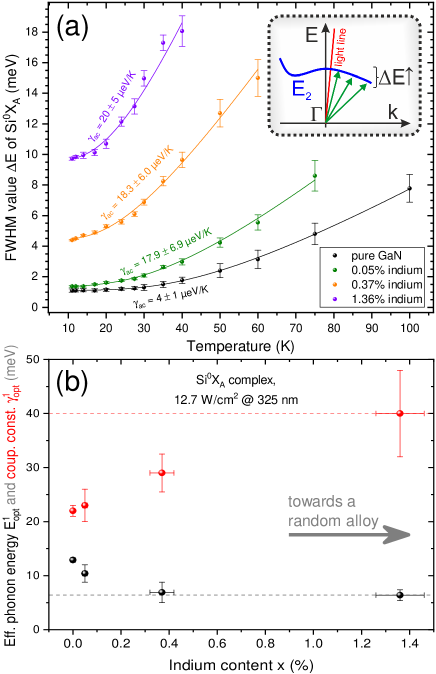
In the following, we will show that the impurity bound exciton complex also provides an extremely versatile tool to study the formation of dilute indium assemblies in GaN:In. While the temperature-dependent linewidth of does not show any clear indium content dependent trend (see Fig. S3), the broadening of upon rising temperature increases with as shown in Fig. 4(a) - a quite unexpected finding in the light of previous alloy studies Goede et al. (1978). In addition to the data shown in Fig. 4, SI Secs. II and III provide an overview about the underlying, temperature-dependent PL spectra and the corresponding analysis of peak positions and linewidths.
Generally, the phonon-induced linewidth broadening is given by
| (3) |
with the acoustical () and the optical () phonon coupling constants as well as the corresponding effective optical phonon energies () numbered by . The best fit to the evolution of shown in Fig. 4(a) for at (solid black line) is obtained for and one set of , values as summarized in Fig. 4(b). Here, is smaller than the energy of the phonon mode in GaN of Callsen et al. (2011). This difference can be explained by the curvature of the corresponding phonon dispersion relation around with as illustrated in the inset of Fig. 4(a). The exciton-phonon coupling related to probes an extended phonon energy interval due to the localization of the bound exciton in real space, providing access to a larger fraction of the first Brillouin zone near the -point. Hence, the temperature-dependent PL data yields an effective phonon energy that is weighted by the corresponding one-phonon density of states Davydov et al. (1998); Pässler (2001); Song et al. (2006).
For the effective phonon energy gradually decreases from to for as depicted in Fig. 4(b). The corresponding fitting parameters denoted in Fig. 4(a) approach values equal to the ones observed for within the given error bars with rising (see Fig. S3 and the corresponding discussion in SI Sec. III). The observed trend for is likely originating from an alloying-induced local variation of the environment. Callsen et al. have found for single excitons trapped in GaN/AlN QDs that, e.g., the exciton-LO-phonon interaction averages over a volume with a radius on the order of Callsen et al. (2015a). Hence, alloying in thick InGaN epilayers can not only directly be monitored by emission energy shifts (see Fig. 2) caused by the immediate indium atom configuration in the vicinity of impurities, which in total leads to the formation of bound excitons. More indirectly, the interaction of bound excitons with phonons can also be used as an alloy probe as shown in Fig. 4.
As for does not show any pronounced indium content dependence (see Fig. S3), we suggest that the environment of centers is richer in indium atoms, a feature only noticeable at the very onset of alloy formation. Thus, here it can be expected that the phonon energies and coupling constants (e.g., and ) will rapidly converge with rising . Any local variation in the indium content caused by the particular distribution of atoms will get increasingly masked by random alloy fluctuations with rising . As a signature of this masking, converges towards as shown in Fig. 4(b). The optical phonon coupling constant continuously rises with , but exhibits an opposite convergence behavior in Fig. 4(b) at the onset of alloy formation. Indium atoms that surround the center within can act as strongly localized isoelectronic centers, whose broad combined distribution in -space seems to foster the interaction with phonons that deviate from the Brillouin zone center. Therefore, the aforementioned bowing of the associated phonon dispersion relation () leads to an effective reduction of the measured values that is accompanied by a rise in . Clearly, the total reduction in the effective phonon energy cannot exclusively be explained by a local rise in indium content as even pure InN still exhibits an phonon energy of around Davydov et al. (1999). In addition, non-dilute indium assemblies matching the size of could have been detected by APT in state-of-the-art InGaN/GaN QW samples Cerezo et al. (2007); Galtrey et al. (2007) commonly comprising silicon concentrations (cf. SI Sec. I). Thus, as a possible reason for the local indium enrichment in the vicinity of centers, we suggest tensile strain that is commonly introduced upon silicon doping of GaN Nenstiel et al. (2015). Hence, it is energetically more favorable for a rather large atom like indium to incorporate close to a silicon atom (distance on the order of ), in order to approach the lattice’s strain equilibrium at the onset of the alloy formation. Bezyazychnaya et al. have theoretically predicted the impact of point defects (vacancies) in InGaN and InGaAs on the indium distribution in these alloys Bezyazychnaya et al. (2015). Here, we experimentally find - to a certain degree - a similar situation for the impurity. Future theoretical work is needed to validate this picture of a point defect embedded in a dilute assembly of indium atoms. This image differs from the common concept of direct complex formation Liu et al. (2016b) that often just considers nearest- or second-nearest-neighbor sites on the cationic sub-lattice.
III.3 Individual bound excitonic complexes analyzed by micro-photoluminescence
Fortunately, -PL measurements with an excitation spot diameter can provide more detailed information regarding the particular configurations of indium atoms close to a donor at the onset of alloy formation. Even on completely unprocessed samples one can resolve individual emission lines around the transition for and partially for 1.36% as show in Fig. 5(a), while the emission remains a rather unstructured emission band due to the given probe volume and excitation power density (). This observation is of high importance as the subsequently described processing of metal apertures on the sample could lead to exciton localization by any damage to the sample as discussed in SI Sec. IV.
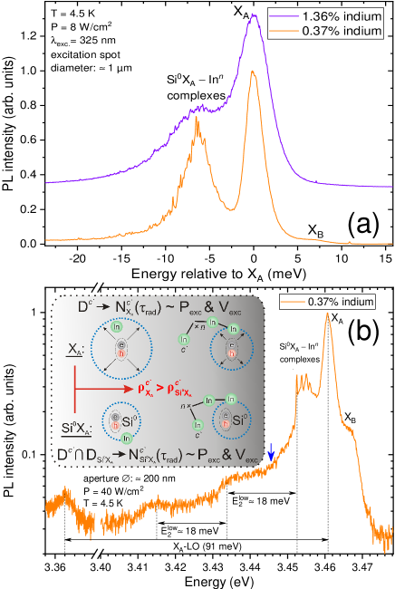
We further reduced the size of the probe volume by processing apertures into an aluminum film with diameters down to on the sample with . As a result, a set of spectrally well separated emission lines can be resolved around along with particular phonon sidebands as shown in Fig. 5(b). An equally spaced ( 18 meV) double step appears on the low energy side of the set of sharp emission lines due to coupling with phonons. Interestingly, the optical signature of the exciton-phonon coupling does not appear as a commonly observed Callsen et al. (2012) isolated peak [see the LO-replica of in Fig. 5(b)], but as a step due to the energetically broad range of contributing phonons with symmetry. About 7 meV below the first step related to the zero phonon lines in the spectrum of Fig. 5(b) (marked by a blue arrow) one even observes an additional, step-like increase in intensity and hence phonon coupling strength in accordance with the findings of Fig. 4(b) ( for ). Hence, the -PL spectrum shown in Fig. 5(b) represents a coarse probe of the phonon density of states that stands in direct relation to the homogeneous broadening of the complex introduced in Fig. 4(a).
The sharp emission lines from Fig. 5(b) present the most direct evidence for an alloying-induced perturbation of the immediate environment at . Here, emission lines with a linewidth of just 320 30 eV can be resolved, opening the perspective for a spectroscopic study of the environment at the nanometer scale based on the emission of such dilute assemblies. In contrast to , the emission remains an unstructured band in our -PL spectra as the density of that attach to a specific indium atom configuration with indium atoms is comparably larger than the corresponding density of centers with an identical configuration of indium atoms in their vicinity.
Generally, the number of any (transition from ) per time interval decaying, indium-related complex is proportional to the -PL excitation volume as well as pump power ( and ) and depends on the corresponding radiative decay time . However, for the case of impurity bound excitons, as illustrated in the inset of Fig. 5(b), the intersecting set of a certain distribution of exemplary indium configurations (e.g., ) and centers () defines the total number of experimentally accessible complexes () via . However, in this simplified description no varying distances are considered in between these sites. Here, could represent a meaningful upper limit for the distance in between a certain indium configuration and the center. Our experimental findings from Sec. III.4 will further elucidate this point.
Hence, only the emission band falls apart into individual emission lines in the -PL spectra of Fig. 5, while a similar observation for would require an even lower excitation density or a smaller probe volume. For instance, the impact of individual indium atoms on the emission of could possibly be resolved for smaller indium concentrations (e.g., ). However, the temperature-induced emission line shifts shown in Fig. S1 and summarized in Fig. S2 (comparison in between ) suggest corresponding values . Hence, the emission energy difference in between, e.g., and centers at cannot straightforwardly be resolved with the present emission linewidths in our samples (eV). So far the impact of individual indium atoms can only be monitored by the localization onset of as demonstrated in Figs. 3(a) and 3(b) based on PL measurements.
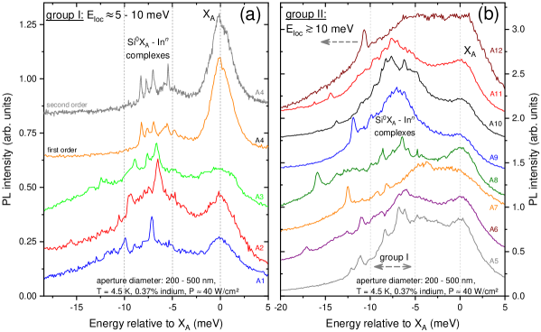
III.4 Statistical analysis of individual bound excitonic complexes
The observation of sharp emission lines in Fig. 5 caused by dilute assemblies directly evokes the need for a statistical analysis of the underlying emitters. Figure 6(a) shows selected -PL spectra recorded for four different metal apertures labeled A1-A4. Here, the two spectra for aperture A4 (measured using the first and second order of the optical grating) provide a detailed view of the -PL spectrum shown in Fig. 5(b). All spectra in Fig. 6(a) show a common optical signature of sharp emission lines related to dilute assemblies in addition to a rather unstructured emission band related to . For the latter case, a smaller spectroscopic probe would be required in order to resolve any spectral details. The localization energy (energetic spacing between and the complexes) commonly ranges in between . Figure 6(b) introduces eight additional -PL spectra (A5-A12) that also show emission lines with that we assign to group II. Generally, the emission lines of group I occur more frequently than their group II counterparts. While almost all spectra in Fig. 6 show emission lines below (partially overlapping likely due to a high density of the associated excitonic complexes), only a few apertures show a clear signature of the emission lines of group II. Here, apertures A5-A12 illustrate the rare cases of these group II emission lines that we extracted from -PL measurements on more than apertures.
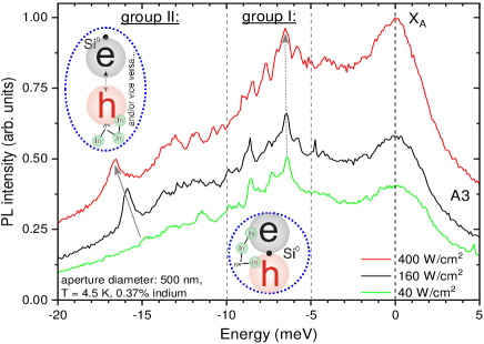
The classification of the sharp emission lines into two groups, I and II, becomes clearer based on Fig. 7, showing excitation power dependent -PL spectra for aperture A3. This excitation power series shows a sequence of spectra that is typical for all apertures showing emission lines of groups I and II. When varying the excitation power density by a factor of ten, group I emission lines only exhibit minor energetic shifts on the order of . In contrast, the emission line of group II from Fig. 7 shifts by towards lower energies.
The emission lines of group I seem to behave like common bound excitons in GaN upon rising excitation power that do not exhibit any pronounced energetic shifts Šantic et al. (1997). The effects of bandgap renormalization and band filling almost perfectly compensate each other over a wide excitation range in GaN, hence, only negligible shifts of bound excitons are noticeable Reynolds et al. (2000). At the given low indium concentration of 0.37% (cf. Figs. 6 and 7) we do not expect any strong deviation from this common behavior of bulk GaN. Hence, we assume that the emission lines of group I belong to complexes comprising a unique configuration of indium atoms within the Bohr radius of the exciton . In this respect, the two electrons and the single hole of this complex occupy a well-defined region and can therefore be referred to as spatially direct, neutral, complex bound excitons as sketched in Fig. 7 for group I. Here in Fig. 7 an exemplary dilute assembly of indium atoms is sketched, along with the center and the most relevant charge carriers.
The pronounced redshift of the emission lines belonging to group II points towards a gradual change in the effective Coulomb interaction in between the charge particles that contribute to the overall emission. A spatially indirect transition as drawn in Fig. 7 for group II could explain such a particular sensitivity to the excitation power as well as the larger values with respect to the emission lines of group I. Clearly, with rising such spatially indirect transitions involving complexes with increasing size and density become more probable. At first glance, the observation of group II emitters resembles the common picture of excitons trapped in -plane (In)GaN QDs that are embedded in, e.g., AlxGa1-xN (0 1) as the matrix material Kindel (2010). Charge fluctuations commonly occur in the matrix material due to point defects, which in-turn leads to a pronounced linewidth broadening known to be particularly strong in III-nitrides Kindel et al. (2014). Upon changing the laser excitation power, the occupation probability of charges in the vicinity of such QDs is altered. As a result of this statistical process, a pronounced red-shift of single QD emission lines can be observed with rising excitation power Kindel (2010); Holmes et al. (2015), which resembles the emission line shift of the group II emitter from Fig. 7. Hence, the pronounced energetic shift of group II emission lines upon varying excitation power could originate from a spectral diffusion phenomenon, which scales with the size of the excitonic dipole moment Kindel et al. (2014). Clearly, indirect excitonic transitions as sketched in Fig. 7 exhibit a larger excitonic dipole moment and are consequently more sensitive to charge fluctuations. Future work should analyze if any preferential orientation exists for this excitonic dipole. However, currently, a more detailed analysis of these group II emitters is hindered by the comparably long integration times for spectra on the order of tens of minutes and the spectral overlap with other emitters, preventing a detailed linewidths and emission line jitter analysis.
IV Discussion
More detailed -PL measurements need to be performed based on further optimized samples in order to reach a conclusive picture regarding the sharp emission lines shown in Figs. 5 - 7. In addition, future temperature-dependent -PL measurements should provide further insights. So far we only observed that the emission lines summarized in Fig. 6 rapidly broaden and thermalize (traceable up to ) due to the associated exciton-phonon coupling involving the mode and acoustic phonons as described for Figs. 4 and 5 (not shown). The distinction made between emission lines of group I and II is mainly motivated by experiments and helps to access the mechanisms of alloying. Generally, a continuous transition can be expected in between these two groups of emission lines, e.g., with rising the probability for spatially indirect transitions should first increase in the dilute alloy limit.
The appearance of spatially direct and indirect recombinations is likely interlinked with the -dependence of the homogeneous linewidth broadening (see Eq. 3) shown in Fig. 4(a). Spatially more indirect transitions exhibit larger excitonic dipole moments that would enable a strong coupling to, e.g., polar phonons like LO-phonons via the Fröhlich interaction Callsen et al. (2015b). However, the limited values of render the contribution of the exciton-LO-phonon coupling negligible in the present temperature range (due to the large LO-phonon energies in nitrides Davydov et al. (1999); Callsen et al. (2011)) and the coupling to acoustic and non-polar, e.g., phonons becomes most relevant as introduced in the context of Fig. 4. The associated exciton-phonon interaction is dominated by the deformation potential coupling, which does not depend on the excitonic dipole moment. In addition, a less prominent piezoelectric coupling will occur Ostapenko et al. (2012). Hence, we can expect complexes with large values (group II) to be more temperature-stable Meyer et al. (2010) than their group I counterparts as long as a dominant contribution of LO-phonons can be excluded. Therefore, with rising temperature the overall emission band related to should first become increasingly influenced by complexes with effectively larger values (group II), while the more spatially direct recombination channels (group I) should preferentially dissociate. However, already at 12 K the emitters of group II seem to increasingly contribute to the linewidth broadening of with rising . Thus, the offset in between the associated experimental values and the model (solid red line) increases with as shown in Fig. 3(a). Finally, the evolution of the weighting in between spatially direct and indirect centers is likely involved in the indium content dependence of at the onset of the alloy formation. Finally, we suggest a twofold reasoning for the particular evolution of : At the onset of alloy formation one can observe a local indium enrichment in the vicinity of centers that affects the exciton-phonon coupling. In addition, spatially direct and indirect transitions exhibit different thermalization behaviors, contributing to the particular evolution of .
V Conclusions
In summary, we have demonstrated the detailed spectroscopic analysis of a III-V mixed crystal alloy by PL and -PL constituting a macro- and even microscopic material characterization. Thus, the present work on a class II alloy approaches the high level of spectroscopic sophistication known for class I alloys that relies on the emission of excitons bound to isoelectronic centers. As no such strongly localized excitons appear in the investigated InxGa1-xN epilayers (0 2.4%), we utilized shallow impurities forming bound states as a tool to study the particular distribution of isoelectronic centers at the onset of alloy formation. By means of -PL we directly observed a hierarchy of bound excitons related to dilute silicon-indium assemblies as individual, energetically sharp (FWHM 300 eV) emission lines appear. Consequently, we introduced a classification of the underlying emitters into spatially direct and indirect bound excitonic complexes, whose balance is weighted by the indium-induced localization of charge carriers at the very onset of alloy formation. However, not only such -PL data, but even conventional macro PL spectra allowed us to extract crucial material parameters for the mixed crystal alloy at hand. Based on ensembles of impurity bound excitons (three-particle complexes) we studied the indium-enriched environment of neutral silicon donors in InGaN at the length scale of the exciton Bohr radius. The analysis of the related exciton phonon coupling revealed a reduction of the average optical phonon energy that governs the temperature-dependent emission line broadening from to upon rising indium content from pure GaN up to . Interestingly, for we found an alloying dependence for the homogeneous emission line broadening caused by local indium enrichment and an indium-induced delocalization of the bound exciton yielding a transition from spatially direct to indirect transitions excitonic complexes. Based on the luminescence traces of free excitons that become increasingly trapped upon alloy formation, we extracted microscopic material properties from conventional PL data. We motivated that upon increasing indium content the radius of the excitonic averaging volume reduces gradually from at down to at . This transition illustrates the evolution from a free exciton in a doped semiconductor to a bound exciton (two-particle complex) in a class II alloy. As a result, the exciton capture by point- and structural defects will be diminished, supporting the high values of the InGaN alloy even at defect densities that are detrimental for other III-V binary semiconductors and alloys like, e.g, (In)GaAs Nozawa and Horikoshi (1991); Chichibu et al. (2006a), AlInGaP Stringfellow and Craford (1998), and AlGaAs Schubert et al. (1984); Chichibu et al. (2006a). Based on our detailed linewidth analysis we estimated that 10 indium atoms are required to form assemblies capable of effectively capturing an exciton at a temperature of 12 K. In contrast, a single indium atom does not introduce an electronic state in the bandgap of InGaN as confirmed by our PL experiments and first theoretically predicted by Bellaiche et al. Bellaiche et al. (1999). Clearly, this justifies the categorization of InGaN as a class II alloy. The present results open the perspective to utilize ensembles, but also individual excitonic complexes as a beneficial tools for any class II alloy analysis at the few nanometer scale. In this regard, our results are not limited to the InGaN alloy. However, the constraints regarding a suitable doping interval are strict and explain - to the best of our knowledge - the absence of corresponding data in the literature for any other class II alloys.
Acknowledgments
This work is supported by the Marie Skłodowska-Curie action ”PhotoHeatEffect” (Grant No. 749565) within the European Union’s Horizon 2020 research and innovation program. The authors wish to thank I. M. Rousseau for his support with the experimental setup. Furthermore, we highly acknowledge D. Martin for growing the samples and K. Shojiki for processing the metal apertures.
References
- Czaja (1971) W. Czaja, Festkörperprobleme XI, Advances in Solid State Physics, edited by O. Madelung (Pergamon, Vieweg, Marburg, Braunschweig, 1971) pp. 65–85.
- Thomas (1966) D. G. Thomas, J. Phys. Soc. Japan 21, 265 (1966).
- Thomas et al. (1965) D. G. Thomas, J. J. Hopfield, and C. J. Frosch, Physical Review Letters 15, 857 (1965).
- Zhang et al. (2000) Y. Zhang, B. Fluegel, A. Mascarenhas, H. Xin, and C. Tu, Physical Review B 62, 4493 (2000).
- Faulkner and Dean (1970) R. A. Faulkner and P. J. Dean, Journal of Luminescence 1, 2, 552 (1970).
- Francoeur et al. (2008) S. Francoeur, S. Tixier, E. Young, T. Tiedje, and A. Mascarenhas, Physical Review B 77, 085209 (2008).
- Wolford (1979) D. Wolford, Journal of Luminescence 18/19, 863 (1979).
- Merz (1968) J. L. Merz, Physical Review 176, 961 (1968).
- Fukushima and Shionoya (1976) T. Fukushima and S. Shionoya, Japanese Journal of Applied Physics 15, 813 (1976).
- Cullen et al. (2013) J. Cullen, K. Johnston, D. Dunker, E. McGlynn, D. R. Yakovlev, M. Bayer, and M. O. Henry, Journal of Applied Physics 114, 193515 (2013).
- Faulkner (1968) R. A. Faulkner, Physical Review 175, 991 (1968).
- Phillips (1969) J. C. Phillips, Physical Review Letters 22, 285 (1969).
- Allen (1971) J. W. Allen, Journal of Physics C: Solid State Physics 4, 1936 (1971).
- Braunstein et al. (1958) R. Braunstein, A. R. Moore, and F. Herman, Physical Review 109, 695 (1958).
- Tietjen and Weisberg (1965) J. J. Tietjen and L. R. Weisberg, Applied Physics Letters 7, 261 (1965).
- Laurenti et al. (1988) J. P. Laurenti, P. Roentgen, K. Wolter, K. Seibert, H. Kurz, and J. Camassel, Physical Review B 37, 4155 (1988).
- Schubert et al. (1984) E. F. Schubert, E. O. Göbel, Y. Horikoshi, K. Ploog, and H. J. Queisser, Physical Review B 30, 813 (1984).
- Butté et al. (2018) R. Butté, L. Lahourcade, T. K. Uždavinys, G. Callsen, M. Mensi, M. Glauser, G. Rossbach, D. Martin, J.-F. Carlin, S. Marcinkevičius, and N. Grandjean, Applied Physics Letters 112, 032106 (2018).
- Wagener et al. (2004) M. C. Wagener, G. R. James, A. W. R. Leitch, and F. Omnès, Phys. Stat. Sol. (c) 1, 2322 (2004).
- Goede et al. (1978) O. Goede, L. John, and D. Hennig, Physica Status Solidi B 89, K183 (1978).
- Klochikhin et al. (1999) A. Klochikhin, A. Reznitsky, S. Permogorov, T. Breitkopf, M. Grün, M. Hetterich, C. Klingshirn, V. Lyssenko, W. Langbein, and J. M. Hvam, Physical Review B 59, 947 (1999).
- Grundmann and Dietrich (2009) M. Grundmann and C. P. Dietrich, Journal of Applied Physics 106, 123521 (2009).
- Bellaiche et al. (1999) L. Bellaiche, T. Mattila, L. W. Wang, S. H. Wei, and A. Zunger, Applied Physics Letters 74, 1842 (1999).
- Dean (1970) P. J. Dean, Journal of Luminescence 1, 398 (1970).
- Kanzaki and Sakuragi (1969) H. Kanzaki and S. Sakuragi, Journal of the Physical Society of Japan 27, 109 (1969).
- Hopfield et al. (1966) J. J. Hopfield, D. G. Thomas, and R. T. Lynch, Physical Review 17, 312 (1966).
- Thomas and Hopfield (1966) D. G. Thomas and J. J. Hopfield, Physical Review 150, 680 (1966).
- Muller et al. (2006) A. Muller, P. Bianucci, C. Piermarocchi, M. Fornari, I. C. Robin, R. André, and C. K. Shih, Physical Review B 73, 081306(R) (2006).
- Manfra (2014) M. J. Manfra, Annual Review of Condensed Matter Physics 5, 347 (2014).
- Stringfellow and Craford (1998) G. B. Stringfellow and M. G. Craford, High Brightness Light Emitting Diodes: Vol 48 (Semiconductors and Semimetals) (Academic Press Inc., San Diego, 1998).
- Chichibu et al. (2006a) S. F. Chichibu, A. Uedono, T. Onuma, B. A. Haskell, A. Chakraborty, T. Koyama, P. T. Fini, S. Keller, S. P. DenBaars, J. S. Speck, U. K. Mishra, S. Nakamura, S. Yamaguchi, S. Kamiyama, H. Amano, I. Akasaki, J. Han, and T. Sota, Nature Materials 5, 810 (2006a).
- Kneissl et al. (2011) M. Kneissl, T. Kolbe, C. Chua, V. Kueller, N. Lobo, J. Stellmach, A. Knauer, H. Rodriguez, S. Einfeldt, Z. Yang, N. M. Johnson, and M. Weyers, Semiconductor Science and Technology 26, 014036 (2011).
- Gil (2014) B. Gil, Physics of Wurtzite Nitrides and Oxides - Passport to Devices (Springer, Heidelberg, 2014).
- Nakamura et al. (1991) S. Nakamura, T. Mukai, and M. Senoh, Japanese Journal of Applied Physics 30, L1998 (1991).
- Nakamura et al. (1997) S. Nakamura, S. Pearton, and G. Fasol, The Blue Laser Diode (Springer, Berlin, 1997).
- Mishra et al. (2008) U. K. Mishra, L. Shen, T. E. Kazior, and Y.-f. Wu, Proceedings of the IEEE 96, 287 (2008).
- Rajan and Jena (2013) S. Rajan and D. Jena, Semiconductor Science and Technology 28, 070301 (2013).
- Wächter et al. (2011) C. Wächter, A. Meyer, S. Metzner, M. Jetter, F. Bertram, J. Christen, and P. Michler, Physica Status Solidi (B) 248, 605 (2011).
- Nippert et al. (2016) F. Nippert, S. Y. Karpov, G. Callsen, B. Galler, T. Kure, C. Nenstiel, M. R. Wagner, M. Straßburg, H. J. Lugauer, and A. Hoffmann, Applied Physics Letters 109, 161103 (2016).
- Ponce and Bour (1997) F. A. Ponce and D. P. Bour, Nature 386, 351 (1997).
- Hangleiter et al. (2005) A. Hangleiter, F. Hitzel, C. Netzel, D. Fuhrmann, U. Rossow, G. Ade, and P. Hinze, Physical Review Letters 95, 127402 (2005).
- Narukawa et al. (1997) Y. Narukawa, Y. Kawakami, M. Funato, S. Fujita, S. Fujita, and S. Nakamura, Applied Physics Letters 70, 981 (1997).
- Kent and Zunger (2001) P. R. C. Kent and A. Zunger, Applied Physics Letters 79, 1977 (2001).
- Galtrey et al. (2007) M. J. Galtrey, R. A. Oliver, M. J. Kappers, C. J. Humphreys, D. J. Stokes, P. H. Clifton, and A. Cerezo, Applied Physics Letters 90, 061903 (2007).
- Cerezo et al. (2007) A. Cerezo, P. H. Clifton, M. J. Galtrey, C. J. Humphreys, T. F. Kelly, D. J. Larson, S. Lozano-Perez, E. A. Marquis, R. A. Oliver, G. Sha, K. Thompson, M. Zandbergen, and R. L. Alvis, Materials Today 10, 36 (2007).
- Rigutti et al. (2018) L. Rigutti, B. Bonef, J. Speck, F. Tang, and R. A. Oliver, Scripta Materialia 148, 75 (2018).
- Mathieu et al. (1992) H. Mathieu, P. Lefebvre, and P. Christol, Physical Review B 46, 4092 (1992).
- Kalceff and Phillips (1995) M. A. S. Kalceff and M. R. Phillips, Physical Review B 52, 3122 (1995).
- Tanimura and Itoh (1981) K. Tanimura and N. Itoh, Journal of Physics and Chemistry of Solids 42, 901 (1981).
- Viswanath et al. (1998) A. K. Viswanath, J. I. Lee, D. Kim, C. R. Lee, and J. Y. Leem, Physical Review B 58, 16333 (1998).
- Onuma et al. (2009) T. Onuma, T. Shibata, K. Kosaka, K. Asai, S. Sumiya, M. Tanaka, T. Sota, A. Uedono, and S. F. Chichibu, Journal of Applied Physics 105, 023529 (2009).
- Zimmermann (1990) R. Zimmermann, Journal of Crystal Growth 101, 346 (1990).
- Vurgaftman and Meyer (2003) I. Vurgaftman and J. R. Meyer, Journal of Applied Physics 94, 3675 (2003).
- Callsen et al. (2018) G. Callsen, T. Kure, M. R. Wagner, R. Butté, and N. Grandjean, Journal of Applied Physics 123, 215702 (2018).
- Šantic et al. (1997) B. Šantic, C. Merz, U. Kaufmann, R. Niebuhr, H. Obloh, and K. Bachem, Applied Physics Letters 71, 1837 (1997).
- Monemar et al. (2001) B. Monemar, W. M. Chen, P. P. Paskov, T. Paskova, G. Pozina, and J. P. Bergman, Physica Status Solidi B 228, 489 (2001).
- Wysmołek et al. (2003) A. Wysmołek, M. Potemski, K. Pakuła, J. M. Baranowski, I. Grzegory, S. Porowski, G. Martinez, and P. Wyder, Physical Review Letters 91, 226404 (2003).
- Fischer et al. (1997) S. Fischer, D. Volm, D. Kovalev, B. Averboukh, A. Graber, H. C. Alt, and B. K. Meyer, Materials Science and Engineering B 43, 192 (1997).
- Claus Klingshirn (2005) Claus Klingshirn, Semiconductor Optics, 2nd ed. (Springer, Berlin Heidelberg New York, 2005).
- Neu et al. (1984) G. Neu, A. A. Mbaye, and R. Triboulet, Proceedings of the 17th International Conference on the Physics of Semiconductors 1, 1029 (1984).
- Gil et al. (2007) B. Gil, P. Bigenwald, M. Leroux, P. P. Paskov, and B. Monemar, Physical Review B 75, 085204 (2007).
- Callsen et al. (2012) G. Callsen, M. Wagner, T. Kure, J. Reparaz, M. Bügler, J. Brunnmeier, C. Nenstiel, A. Hoffmann, M. Hoffmann, J. Tweedie, Z. Bryan, S. Aygun, R. Kirste, R. Collazo, and Z. Sitar, Physical Review B 86, 075207 (2012).
- Wagner et al. (2011) M. R. Wagner, G. Callsen, J. S. Reparaz, J. H. Schulze, R. Kirste, M. Cobet, I. A. Ostapenko, S. Rodt, C. Nenstiel, M. Kaiser, A. Hoffmann, A. V. Rodina, M. R. Phillips, S. Lautenschlaeger, S. Eisermann, and B. K. Meyer, Physical Review B 84, 035313 (2011).
- Chichibu et al. (2006b) S. F. Chichibu, T. Onuma, M. Kubota, A. Uedono, T. Sota, A. Tsukazaki, A. Ohtomo, and M. Kawasaki, Journal of Applied Physics 99, 093505 (2006b).
- Shu et al. (1998) C. K. Shu, J. Ou, H. C. Lin, W. K. Chen, and M. C. Lee, Applied Physics Letters 73, 641 (1998).
- Shen et al. (1999) X. Shen, P. Ramvall, P. Riblet, and Y. Aoyagi, Japanese Journal of Applied Physics 38, L411 (1999).
- Shen and Aoyagi (1999) X.-Q. Shen and Y. Aoyagi, Japanese Journal of Applied Physics 38, L14 (1999).
- Kumano et al. (2001) H. Kumano, K.-i. Hoshi, S. Tanaka, I. Suemune, X.-Q. Shen, P. Riblet, P. Ramvall, and Y. Aoyagi, Applied Physics Letters 75, 2879 (2001).
- Liu et al. (2016a) W. Liu, J.-F. Carlin, N. Grandjean, B. Deveaud, and G. Jacopin, Applied Physics Letters 109, 042101 (2016a).
- Hayama et al. (2017) Y. Hayama, I. Takahashi, and N. Usami, Energy Procedia 124, 734 (2017).
- Callsen et al. (2011) G. Callsen, J. S. Reparaz, M. R. Wagner, R. Kirste, C. Nenstiel, A. Hoffmann, and M. R. Phillips, Applied Physics Letters 98, 061906 (2011).
- Davydov et al. (1998) V. Y. Davydov, Y. E. Kitaev, I. N. Goncharuk, A. N. Smirnov, J. Graul, O. Semchinova, D. Uffmann, M. B. Smirnov, A. P. Mirgorodsky, and R. A. Evarestov, Physical Review B 58, 12899 (1998).
- Pässler (2001) R. Pässler, Journal of Applied Physics 89, 6235 (2001).
- Song et al. (2006) D. Y. Song, M. Basavaraj, S. A. Nikishin, M. Holtz, V. Soukhoveev, A. Usikov, and V. Dmitriev, Journal of Applied Physics 100, 113504 (2006).
- Callsen et al. (2015a) G. Callsen, G. Pahn, S. Kalinowski, C. Kindel, J. Settke, J. Brunnmeier, C. Nenstiel, T. Kure, F. Nippert, A. Schliwa, A. Hoffmann, T. Markurt, T. Schulz, M. Albrecht, S. Kako, M. Arita, and Y. Arakawa, Physical Review B 92, 235439 (2015a).
- Davydov et al. (1999) V. Y. Davydov, V. V. Emtsev, I. N. Goncharuk, A. N. Smirnov, V. D. Petrikov, V. V. Mamutin, V. A. Vekshin, S. V. Ivanov, M. B. Smirnov, and T. Inushima, Applied Physics Letters 75, 3297 (1999).
- Nenstiel et al. (2015) C. Nenstiel, M. Bügler, and G. Callsen, Physica Status Solidi (RRL) 9, 716 (2015).
- Bezyazychnaya et al. (2015) T. V. Bezyazychnaya, D. M. Kabanau, V. V. Kabanov, Y. V. Lebiadok, A. G. Ryabtsev, G. I. Ryabtsev, V. M. Zelenkovskii, and S. K. Mehta, Lithuanian Journal of Physics 55, 10 (2015).
- Liu et al. (2016b) Z. Liu, B. Fu, X. Yi, G. Yuan, and J. Wang, RSC Advances 6, 5111 (2016b).
- Reynolds et al. (2000) D. C. Reynolds, D. C. Look, and B. Jogai, Journal of Applied Physics 88, 5760 (2000).
- Kindel (2010) C. H. Kindel, Study on Optical Polarization in Hexagonal Gallium Nitride Quantum Dots, Ph.D. thesis, University of Tokyo (2010).
- Kindel et al. (2014) C. Kindel, G. Callsen, S. Kako, T. Kawano, H. Oishi, G. Hönig, A. Schliwa, A. Hoffmann, and Y. Arakawa, Phys Status Solidi - Rapid Research Letters 8, 408 (2014).
- Holmes et al. (2015) M. Holmes, S. Kako, K. Choi, M. Arita, and Y. Arakawa, Physical Review B 92, 115447 (2015).
- Callsen et al. (2015b) G. Callsen, G. Pahn, S. Kalinowski, C. Kindel, J. Settke, J. Brunnmeier, C. Nenstiel, T. Kure, F. Nippert, A. Schliwa, A. Hoffmann, T. Markurt, T. Schulz, M. Albrecht, S. Kako, M. Arita, and Y. Arakawa, Physical Review B 92, 235439 (2015b).
- Ostapenko et al. (2012) I. A. Ostapenko, G. Hönig, S. Rodt, A. Schliwa, A. Hoffmann, D. Bimberg, M. R. Dachner, M. Richter, A. Knorr, S. Kako, and Y. Arakawa, Physical Review B 85, 081303(R) (2012).
- Meyer et al. (2010) B. K. Meyer, J. Sann, S. Eisermann, S. Lautenschlaeger, M. R. Wagner, M. Kaiser, G. Callsen, J. S. Reparaz, and A. Hoffmann, Physical Review B 82, 115207 (2010).
- Nozawa and Horikoshi (1991) K. Nozawa and Y. Horikoshi, Japanese Journal of Applied Physics 30, L668 (1991).