Quantum electron transport in ohmic edge contacts between two-dimensional materials
Abstract
The metal-semiconductor contact is a major factor limiting the shrinking of transistor dimension to further increase device performance. In-plane edge contacts have the potential to achieve lower contact resistance due to stronger orbital hybridization compared to conventional top contacts. However, a quantitative understanding of the electron transport properties in the edge contact is still lacking. In this work, we present full-band atomistic quantum transport simulations of the graphene/\chMoS2 edge contact. By using a Wannier function basis to accurately describe the electronic bands, together with a full self-consistent solution of the electrostatics, we are able to efficiently model device structures on a micron scale, but with atomic level accuracy. We find that the potential barrier created by trapped charges decays fast with distance away from the interface, and is thus thin enough to enable efficient injection of electrons. This results in Ohmic behavior in its I-V characteristics, which agrees with experiments. Our results demonstrate the role played by trapped charges in the formation of a Schottky barrier, and how one can reduce the Schottky barrier height (SBH) by adjusting the relevant parameters of the edge contact system. Our framework can be extended conveniently to incorporate more general nanostructure geometries. For example, a full 3D solution of the electrostatics will also lead to better modeling of the electrical potential. Furthermore, better ab-initio calculations can be conveniently added to our methods to further improve their accuracy.
keywords:
2D material, edge contacts, electron transport, self-consistent simulations, electrostatics, ohmic I-V characteristicsThe University of Chicago] James Franck Institute and Department of Physics, The University of Chicago, Chicago, Illinois 60637, United States The University of Chicago] James Franck Institute and Department of Physics, The University of Chicago, Chicago, Illinois 60637, United States \alsoaffiliation[Argonne National Laboratory] Materials Science Division, Argonne National Laboratory, Lemont, Illinois 60439, United States \abbreviations
Two-dimensional (2D) materials such as graphene and transition metal dichalcogenides (TMDCs) are pushing the forefront of complementary metal-oxide semiconductor (CMOS) technology beyond the Moore’s law 1, 2, and show great promises for realizing atomically thin circuitry 3, 4, 5. A fundamental challenge to their effective use remains the large resistance of electrical contacts to 2D materials for probing and harnessing their novel electronic properties 6, 7, 8. There are generally two types of contact geometries, namely top contacts and edge contacts 6. Conventional 3D metallic top contacts can achieve low contact resistance with monolayer 2D materials, but cannot avoid the intrinsic problem of large electrode volume. 9, 10, 6, 11 2D top contacts, including graphene 12, 13, 14 and recently demonstrated atomically flat metal thin films 11, can achieve both small volumes and low contact resistances of metal-semiconductor interfaces, but they suffer from weak van der Waals coupling to TMDCs 15. Their transfer efficiency depends largely on the contact area and is compromised dramatically below a transfer length which is typically tens of nm scale 16, 8. In contrast, 2D edge contacts are formed by joining atomically thin metal electrodes and semiconductors laterally in a single plane. They offer the possibilities for high-quality contacts to 2D materials despite minimal contact area defined by their atomic thickness as shown by both simulations 15 and recent experimental successes 16, 17. Among them, the graphene-\chMoS2 system considered in this paper is particularly promising for a low-resistance 2D edge contact 16, 18, 17. According to the Schottky-Mott rule, the combination of a low-work-function metallic graphene electrode and a typical n-type 19 semiconducting monolayer \chMoS2 channel naturally leads to a small SBH. Moreover, the overall system is stable under working conditions and resistant to phase transitions induced by adsorbates. While improving experimental techniques makes more tests feasible, a better quantitative understanding of the electronic structure and transport properties is still critical for improving the design of 2D edge contacts. In 2016, Yu et al. 20 suggested a highly non-localized carrier redistribution and strong reduction of Fermi level pinning in 2D systems based on a semi-classical macroscopic model. In 2017, Chen et al. 21 performed first-principles studies based on density functional theory (DFT) on the morphologies of the graphene/\chMoS2 lateral junction and proposed several stable interface configurations. Sun et al. 22 performed similar studies and tried to calculate the transport efficiencies, but did not reproduce the linear I-V characteristics observed in experiments, possibly due to the lack of doping in the semiconductor region.
In order to better model the graphene/\chMoS2 interface at the atomic scale and quantitatively calculate the charge transfer properties, we introduced a custom-built self-consistent quantum transport solver based on the Keldysh Nonequilibrium Green’s Function formalism 23, 24 and Maximally Localized Wannier functions (MLWFs) 25. Such a method can efficiently solve the local electrostatics and electron transport with first-principles accuracy at a minimal cost of tight-binding calculations. It enables the inclusion of large areas of both materials, which is necessary in order to allow for a long screening length for charged interfacial states and thus to have equilibrium conditions near the edge of the central device region. This is also a necessary condition for the decimation technique to account for the effects of the semi-infinite leads. We find that trapped interface states lead to a potential barrier, which is however small enough that we find Ohmic behavior at room temperature and high enough doping levels. We successfully reproduced the linear current-voltage (I-V) characteristics with a resistivity value of approximately 30 close to that observed in experiments 17 at room temperature, which is a first for 2D edge contact systems. At lower temperatures, We observe increasing non-linearity as a result of reduced thermalization. In the following, we calculate the band structures of graphene and monolayer \chMoS2, and extract their tight-binding parameters using MLWFs. Based on these parameters, we use our custom-built quantum transport solver to generate the electrostatic potential self-consistently with the inhomogeneous charge densities induced by band bending, and by local impurity states. We confirm the validity of our solver by comparing the converged electrostatic potential profile to the analytical predictions from Thomas-Fermi screening theory, beyond angstrom distances from the contact region. Finally, we calculate the transport properties based on the Keldysh formalism and discuss how to further improve device performance.
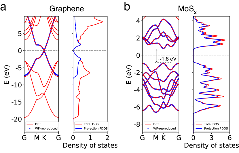
Wannier functions can accurately and efficiently capture delicate electronic structures. We used them to extract the tight-binding parameters of both materials after obtaining the band structures in the DFT framework. Figure 1 compares the band structures obtained with DFT and with the MLWF Hamiltonian for both monolayer graphene and \chMoS2. From the plot, we can see that the Wannier projections work so well that the differences between the two bands are largely unnoticeable. We also compare the total Density of States (DOS) and the Projected Density of States (PDOS) reproduced by the MLWF orbitals for both materials. Instead of using all the orbitals in a unit cell, we choose only those contributing to the DOS near the Fermi level for Wannier projections. This can minimize the sizes of matrices used in our calculations and further reduce computational cost. The extracted hopping parameters then serve as basis for the transport simulations.
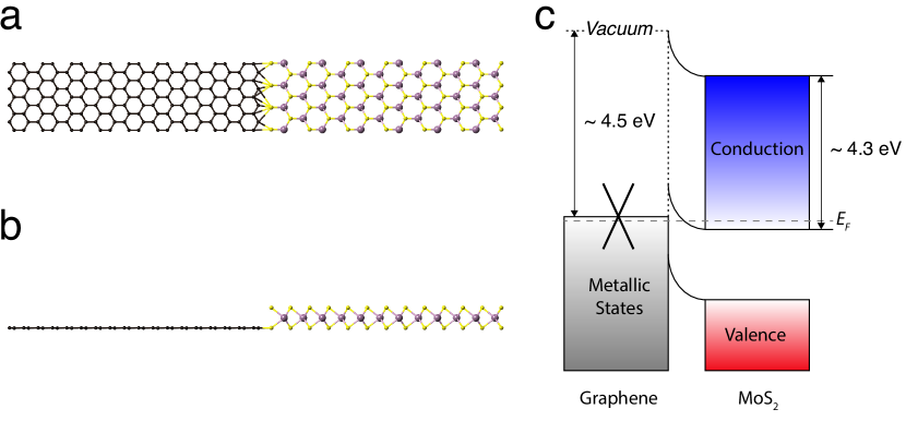
The geometry of the graphene-\chMoS2 edge contact is sketched in Figure 2a and 2b. We assume periodicity of the device in the y direction, at a level of a few unit cells which is long enough to approximately match the lattice constants. As a result, the Hamiltonian shows a dependence and can be decomposed into three components according to the Bloch’s theorem as
| (1) |
where are the interactions within a strip of width, are the interactions with a neighbor strip along the or direction, and is the width of the supercell. To make second-nearest-neighbor interactions negligible, we choose to be exactly times the width of the graphene unit cell, and approximately times that of the \chMoS2 unit cell, resulting in a lattice mismatch of only 4.2%. We do not change the lattice constant of graphene because it has a much larger Young’s modulus 26. For the interface, we consider the predominant zigzag edge of graphene 27 and \chMoS2 28 as shown in Figure 2a and choose a structure motivated by ab initio calculations. According to Chen et al. 21, the configuration chosen in our study has the lowest formation energies among other alternative geometries. We adjust the Fermi level of both materials to match the induced doping by gate voltage. For the details of the parameters used in this study and their effects on the simulation results, please refer to our supporting information. Figure 2c illustrates the band alignments of the edge contact device simulated in this paper. Having established the atomic geometry and band alignments of the junction, we now investigate the electrostatics and charge transfer effects at the boundary.
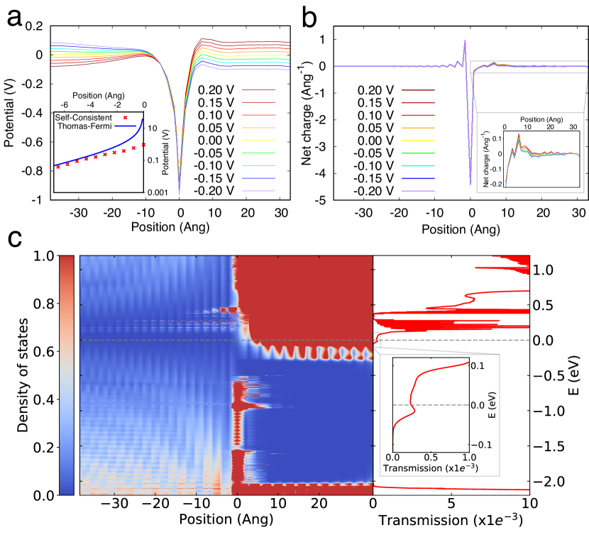
To evaluate the tunneling barrier, we calculate charge densities self-consistently with electrostatic potential for the edge contact device. We use the Nonequilibrium Green’s Function technique based on the Keldysh formalism to calculate the charge densities, and the non-linear Newton-Raphson technique to solve for the electrostatic potential from the Poisson equation. We performed simulations for different source-drain biases at a MoS2 doping level of and at room temperature of . The converged potential and charge profiles are shown in Figure 3a and Figure 3b respectively. We can see that the electrostatic potential reaches equilibrium at both edges of our simulated region. Applied source-drain biases shift the potential level in the two electrodes and in turn modify the net charge profile. In the inset of Figure 3b, we enlarge the plot for the \chMoS2 side to better show how the net charge distribution adapts to the external biases. Here we safely ignored the electron-phonon scattering, due to the short channel length of 2D edge contacts. In order to check the validity of the electrostatics obtained from our self-consistent simulations, we compare the converged potential profile with the analytical predictions of a quasi-1D Thomas-Fermi screening potential, and the result is shown in the inset of Figure 3a. We find that the two results agree well beyond angstrom distances from the contact region, where the charge densities can stay low enough for the Thomas-Fermi theory to work well. This confirms the accuracy of our method. The derivations of the quasi-1D Thomas-Fermi screening potential are given in the supporting information.
Using the converged electrostatic profiles, we further examine the quantum transport properties of the graphene-\chMoS2 edge contact by calculating its Local Density of States (LDOS) and transmission spectrum using the Landauer-Buttiker formalism. The transmission coefficients are determined by the equation:
| (2) |
where and are the linewidth functions that describe the coupling between the scattering region and the two leads on the left and right. In Figure 3c, We show the two results under room temperature and zero bias side by side.
From the results in Figure 3, we find that the electrostatic potential is screened by the electrons and decays fast as one goes away from the interface, which allows charge carriers to tunnel through the boundary efficiently. When the metallic graphene contacts with monolayer \chMoS2 contacts, free electrons will flow from the graphene side to the \chMoS2 side since the work function of p-type graphene is smaller than that of n-type \chMoS2. When the charge redistribution reaches equilibrium, graphene is positively charged whereas \chMoS2 monolayer is negatively charged near the interface region, in which a built-in electric dipole is induced. 29 In addition, trapped charges at the interface produce a monopole, which we find to be substantial. Such electric fields can shift the energy bands of the \chMoS2 monolayer upward. However, we find that the barrier is efficiently screened by the free charges and becomes thin enough for the electrons to tunnel through. From Figure 3c, we can see the two-fold effects of the interfacial bonding: The trapped charges at the interface form a thin potential barrier, which is screened effectively allows electrons to go through; The overlap states serve as a bridge inside the barrier further assisting with charge transfer. As a result, for given parameter settings, no Schottky barrier is present in this case, and we observe sufficient transmission near the Fermi level, indicating the ohmic nature of the graphene-\chMoS2 interface.
To check the reliability of our interface modeling, we integrate the boundary DOS over energy within the band gap of the \chMoS2 interior states, and obtain the number of the interfacial states to be about states . This is close to the full DFT simulation results reported by Chen et al 21 ranging from 6.3 to 8.3 states , and therefore proves the accuracy of our modeling method. However, the ohmic behavior in our simulation requires doping level one order of magnitude larger than the one reported by experiments. One possible explanation is that we only assume electron hopping between graphene supercells and sulfur atoms immediately next to the interface. By considering interactions of longer range, one can make the overlap states couple better with the conduction band. This could potentially improve transport efficiency and lower the needed doping level to achieve ohmic behavior in our simulation. Also, although we find that relative perpendicular positions of the two materials hardly affect the transmission efficiency, other boundary configurations including different edge types (armchair or zigzag) and interface roughness could still alter the positions of the overlap states, and in turn change the tunneling current. We leave a systematic examination of the above factors to future work.
To explore more on the ohmic behavior of graphene-\chMoS2 edge contact, we calculate the source-drain currents under different biases and temperatures. The electric current can be calculated as:
| (3) |
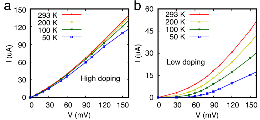
where is the transmission coefficient given by equation (2), is the bias voltage, and is the Fermi distribution function of the left/right lead. In Figure 4a, we find that at a high \chMoS2 doping level of , the I-V curves of the graphene-\chMoS2 edge contact show linear characteristics at room temperature, with ohmic behavior maintained down to temperatures at least as low as 50 K. Moreover, we run the same calculation for a \chMoS2 doping level of , and find non-linear I-V behaviors due to the existence of a large Schottky barrier (see Figure 3b of Supporting Information) at low carrier densities, as shown in Figure 4b. This barrier also leads to smaller currents at lower temperatures because reduced thermalization makes it harder for the electrons to go across the interface, which also agrees with experiment. 17
From Figure 3c, we notice that the resonant levels from graphene edge states can assist in the carrier injection across the interface in the range of 0.1 to 0.5 . One could potentially take advantage of these edge states by adding more n-type doping to graphene and effectively moving down its resonant levels closer to the Fermi level. We verified our prediction by performing simulations with the above changes, and indeed obtained larger transmission values at the Fermi level, as shown in Figure 4 of our Supporting Information. This leads to a lower resistance with a greater source-drain current under the same bias. Therefore, we propose that the usage of an n-doped graphene electrode could be a further improvement to the present edge contact design.
In conclusion, we have developed a computational pipeline to study the electrostatic and transport properties of the 2D graphene-\chMoS2 edge contact, and proposed a possible explanation for its ohmic behavior observed in experiments. By applying the custom-built quantum transport simulation scheme, we obtain the charge density profile self-consistently with the electrostatic potential profile of the device. We find that the potential barrier decays fast away from the interface and is thin enough for the electron to tunnel through efficiently. Our results are consistent with both analytical Thomas-Fermi screening theory and the experimental measurements. Because our methods can be scaled effectively to large systems, but maintain the fidelity of ab initio band structures, they can be used to efficiently predict the electrostatic and transport properties for nanostructures, including those with complex geometries. These findings could have broad implications in the design and fabrication of metal-semiconductor junction for realizing low-resistance contacts.
The authors thank Jiwoong Park and Saptarshi Das for discussions and for comments on an earlier draft of the paper. Research at Argonne is supported by DOE Office of Science, Basic Energy Sciences, Materials Science and Engineering.
The supporting information is available free of charge.
-
•
Transport simulation pipeline
-
•
Band structure calculation and Wannierization
-
•
Self-consistent iteration scheme
-
•
Effects of different parameters on the simulation results
-
•
Derivation of Thomas-Fermi approximation for quasi-1D systems
References
- Neto et al. 2009 Neto, A. C.; Guinea, F.; Peres, N. M.; Novoselov, K. S.; Geim, A. K. The electronic properties of graphene. Reviews of modern physics 2009, 81, 109
- Novoselov et al. 2016 Novoselov, K.; Mishchenko, A.; Carvalho, A.; Neto, A. C. 2D materials and van der Waals heterostructures. Science 2016, 353, aac9439
- Levendorf et al. 2012 Levendorf, M. P.; Kim, C.-J.; Brown, L.; Huang, P. Y.; Havener, R. W.; Muller, D. A.; Park, J. Graphene and boron nitride lateral heterostructures for atomically thin circuitry. Nature 2012, 488, 627
- Fiori et al. 2014 Fiori, G.; Bonaccorso, F.; Iannaccone, G.; Palacios, T.; Neumaier, D.; Seabaugh, A.; Banerjee, S. K.; Colombo, L. Electronics based on two-dimensional materials. Nature nanotechnology 2014, 9, 768
- Duan et al. 2015 Duan, X.; Wang, C.; Pan, A.; Yu, R.; Duan, X. Two-dimensional transition metal dichalcogenides as atomically thin semiconductors: opportunities and challenges. Chemical Society Reviews 2015, 44, 8859–8876
- Allain et al. 2015 Allain, A.; Kang, J.; Banerjee, K.; Kis, A. Electrical contacts to two-dimensional semiconductors. Nature Materials 2015, 14, 1195
- Xu et al. 2016 Xu, Y.; Cheng, C.; Du, S.; Yang, J.; Yu, B.; Luo, J.; Yin, W.; Li, E.; Dong, S.; Ye, P.; Duan, X. Contacts between two-and three-dimensional materials: ohmic, Schottky, and p–n heterojunctions. ACS nano 2016, 10, 4895–4919
- Schulman et al. 2018 Schulman, D. S.; Arnold, A. J.; Das, S. Contact engineering for 2D materials and devices. Chemical Society Reviews 2018,
- Li et al. 2014 Li, S.-L.; Komatsu, K.; Nakaharai, S.; Lin, Y.-F.; Yamamoto, M.; Duan, X.; Tsukagoshi, K. Thickness scaling effect on interfacial barrier and electrical contact to two-dimensional MoS2 layers. ACS nano 2014, 8, 12836–12842
- Liu et al. 2015 Liu, W.; Sarkar, D.; Kang, J.; Cao, W.; Banerjee, K. Impact of contact on the operation and performance of back-gated monolayer MoS2 field-effect-transistors. ACS nano 2015, 9, 7904–7912
- Liu et al. 2018 Liu, Y.; Guo, J.; Zhu, E.; Liao, L.; Lee, S.-J.; Ding, M.; Shakir, I.; Gambin, V.; Huang, Y.; Duan, X. Approaching the Schottky–Mott limit in van der Waals metal–semiconductor junctions. Nature 2018, 557, 1
- Das et al. 2012 Das, S.; Chen, H.-Y.; Penumatcha, A. V.; Appenzeller, J. High performance multilayer MoS2 transistors with scandium contacts. Nano letters 2012, 13, 100–105
- Das et al. 2014 Das, S.; Gulotty, R.; Sumant, A. V.; Roelofs, A. All two-dimensional, flexible, transparent, and thinnest thin film transistor. Nano letters 2014, 14, 2861–2866
- Liu et al. 2015 Liu, Y.; Wu, H.; Cheng, H.-C.; Yang, S.; Zhu, E.; He, Q.; Ding, M.; Li, D.; Guo, J.; Weiss, N. O.; Huang, Y.; Duan, X. Toward barrier free contact to molybdenum disulfide using graphene electrodes. Nano letters 2015, 15, 3030–3034
- Kang et al. 2014 Kang, J.; Liu, W.; Sarkar, D.; Jena, D.; Banerjee, K. Computational study of metal contacts to monolayer transition-metal dichalcogenide semiconductors. Physical Review X 2014, 4, 031005
- Ling et al. 2016 Ling, X. et al. Parallel stitching of 2D materials. Advanced Materials 2016, 28, 2322–2329
- Guimarães et al. 2016 Guimarães, M.; Gao, H.; Han, Y.; Kang, K.; Xie, S.; Kim, C.; Muller, D.; Ralph, D.; Park, J. Atomically thin ohmic edge contacts between two-dimensional materials. ACS nano 2016, 10, 6392–6399
- Zhao et al. 2016 Zhao, M.; Ye, Y.; Han, Y.; Xia, Y.; Zhu, H.; Wang, S.; Wang, Y.; Muller, D. A.; Zhang, X. Large-scale chemical assembly of atomically thin transistors and circuits. Nature nanotechnology 2016, 11, 954
- Lee et al. 2012 Lee, Y.-H.; Zhang, X.-Q.; Zhang, W.; Chang, M.-T.; Lin, C.-T.; Chang, K.-D.; Yu, Y.-C.; Wang, J. T.-W.; Chang, C.-S.; Li, L.-J.; Lin, T. Synthesis of large-area MoS2 atomic layers with chemical vapor deposition. Advanced materials 2012, 24, 2320–2325
- Yu et al. 2016 Yu, H.; Kutana, A.; Yakobson, B. I. Carrier delocalization in two-dimensional coplanar p–n junctions of graphene and metal dichalcogenides. Nano letters 2016, 16, 5032–5036
- Chen et al. 2017 Chen, W.; Yang, Y.; Zhang, Z.; Kaxiras, E. Properties of in-plane graphene/MoS2 heterojunctions. 2D Materials 2017, 4, 045001
- Sun et al. 2017 Sun, J.; Lin, N.; Tang, C.; Wang, H.; Ren, H.; Zhao, X. First principles studies on electronic and transport properties of edge contact graphene-MoS2 heterostructure. Computational Materials Science 2017, 133, 137–144
- Luisier et al. 2006 Luisier, M.; Schenk, A.; Fichtner, W.; Klimeck, G. Atomistic simulation of nanowires in the s p 3 d 5 s* tight-binding formalism: From boundary conditions to strain calculations. Physical Review B 2006, 74, 205323
- Datta 2000 Datta, S. Nanoscale device modeling: the Green’s function method. Superlattices and microstructures 2000, 28, 253–278
- Marzari et al. 2012 Marzari, N.; Mostofi, A. A.; Yates, J. R.; Souza, I.; Vanderbilt, D. Maximally localized Wannier functions: Theory and applications. Reviews of Modern Physics 2012, 84, 1419
- Jiang 2015 Jiang, J.-W. Graphene versus MoS 2: A short review. Frontiers of Physics 2015, 10, 287–302
- Yu et al. 2011 Yu, Q. et al. Control and characterization of individual grains and grain boundaries in graphene grown by chemical vapour deposition. Nature materials 2011, 10, 443
- Lauritsen et al. 2007 Lauritsen, J. V.; Kibsgaard, J.; Helveg, S.; Topsøe, H.; Clausen, B. S.; Lægsgaard, E.; Besenbacher, F. Size-dependent structure of MoS 2 nanocrystals. Nature nanotechnology 2007, 2, 53
- Bristowe et al. 2014 Bristowe, N.; Ghosez, P.; Littlewood, P. B.; Artacho, E. The origin of two-dimensional electron gases at oxide interfaces: insights from theory. Journal of Physics: Condensed Matter 2014, 26, 143201