SkyLogic – A proposal for a skyrmion logic device
Abstract
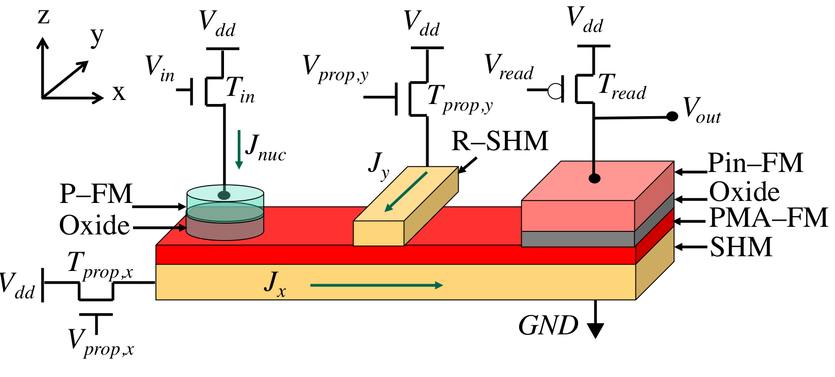
This work proposes a novel logic device (SkyLogic) based on skyrmions, which are magnetic vortex-like structures that have low depinning current density and are robust to defects. A charge current sent through a polarizer ferromagnet (P–FM) nucleates a skyrmion at the input end of an intra-gate FM interconnect with perpendicular magnetic anisotropy (PMA–FM). The output end of the PMA–FM forms the free layer of an MTJ stack. A spin Hall metal (SHM) is placed beneath the PMA–FM. The skyrmion is propagated to the output end of the PMA–FM by passing a charge current through the SHM. The resistance of the MTJ stack is low (high) when a skyrmion is present (absent) in the free layer, thereby realizing an inverter. A framework is developed to analyze the performance of the SkyLogic device. A circuit-level technique is developed that counters the transverse displacement of skyrmion in the PMA–FM and allows use of high current densities for fast propagation. The design space exploration of the PMA–FM material parameters is performed to obtain an optimal design point. At the optimal point, we obtain an inverter delay of ps with a switching energy of fJ.
Index Terms:
Design space exploration, skyrmions, spintronics.I Introduction
Recently, research in spintronics has accelerated in an effort to find an alternative to or complement the existing CMOS-based electronics. Several physical phenomena have been exploited to develop novel spin logic devices [6, 9]. Some of the more successful logic device concepts are based on manipulation of the magnetic nanostructures like domain-walls [7, 8, 11], but domain-walls are susceptible to pinning due to material defects [16]. Recently, skyrmions, which are vortex-like spin structures in magnetic thin films, have been actively studied [4]. Skyrmions have proven to be more robust to pinning compared to domain walls [4]. The recent room temperature experimental observation of skyrmion creation, current-driven displacement, and detection [3], make them attractive structures to develop skyrmion-based logic devices.
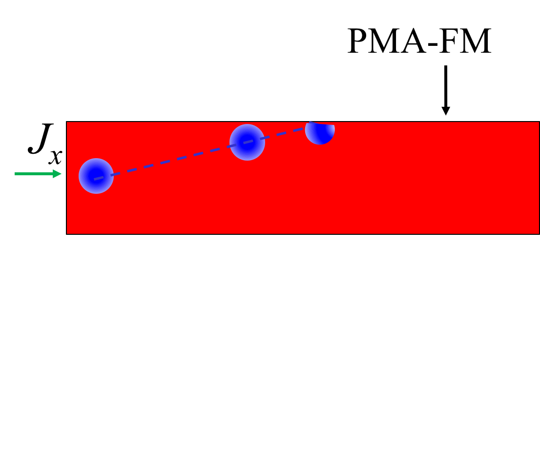
Several skyrmion-based logic devices [23, 24, 15] have been proposed. The skyrmion velocity in these devices is limited by its transverse displacement due to Magnus force [4]. Prior works have considered this effect as a constraint, severely limiting their performance. Magnetic bilayer systems, where the skyrmions nucleated in each of these layers are anti-ferromagnetically coupled to each other [25, 19] such that the Magnus force cancels out, have been proposed. However, in such cases, careful engineering of the materials is required to obtain perfect coupling of the skyrmions.
In this work, we propose a skyrmion-based logic device, SkyLogic. A spin-polarized charge current is injected into a PMA ferromagnet (PMA–FM) to nucleate a skyrmion at the input end. A charge current sent through a high resistivity material, called the spin Hall metal (SHM) placed directly beneath the PMA–FM propagates the skyrmion from the input end to the output end of the PMA–FM. We counter the transverse displacement of the skyrmion from the Magnus effect by sending a charge current through a repeater SHM (R–SHM) placed at intervals above the PMA–FM, and perpendicular to the direction of the SHM. The skyrmion is detected at the output end as a resistance change in the magnetic tunnel junction (MTJ) stack. A charge current sent through the MTJ stack turns the input transistor switch of the next stage SkyLogic on. Depending on the resistance of the MTJ stack, the strength of the charge current nucleates a skyrmion in the next stage, thereby implementing an inverter.
We derive an analytical model to analyze the skyrmion motion through the PMA–FM under the application of the two charge currents. We obtain the delay and energy model of SkyLogic as a function of the PMA–FM material parameters. Next, we perform a systematic design space exploration of the material parameters to optimize the device performance. We show that our novel approach to counter the Magnus force allows the use of large current densities for skyrmion propagation. In addition, our circuit-based solution can be implemented with the existing materials that have been used to demonstrate skyrmion propagation. With the novel design and optimization, we show that it is possible to achieve an inverter delay of ps, with fJ switching energy.
II Overview of the SkyLogic Device
We first propose the SkyLogic device and explain it using an inverter. We then show the design of a two-input NOR (NOR2) gate implemented using SkyLogic.
II-A Design of the SkyLogic Inverter
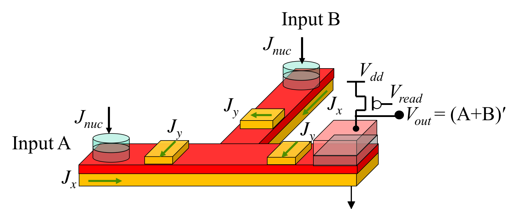
A schematic of our proposed skyrmion–based logic device is shown in Fig. 1 (a), and consists of the following components. At the input end, a polarizer ferromagnet (P–FM) is placed on top of ferromagnetic intra–gate interconnect with perpendicular magnetic anisotropy, PMA–FM, which connects the input to the output of the device. A layer of SHM is placed below the PMA–FM, along its entire length. Another layer of SHM, called the repeater SHM (R–SHM), is placed on top of the PMA–FM between the input and the output in a direction transverse to the PMA–FM. At the output end, the presence of a skyrmion is detected by an MTJ structure. This consists of an oxide layer sandwiched between a ferromagnet with pinned magnetization (Pin–FM) and the output end of the PMA–FM channel. The output end of the PMA–FM acts as the MTJ free layer. The functionality of the device can be understood by examining its operation in stages:
Stage 1 – Skyrmion nucleation: At the input end, a voltage turns a transistor on and sends a charge current with current density . This charge current is spin–polarized by the P–FM [3]. If is greater than a critical current density , the spin-polarized current nucleates a skyrmion in the PMA–FM beneath the P–FM, in time .
Stage 2 – Skyrmion propagation: Once the skyrmion is nucleated, a voltage turns on transistor and sends a charge current with density through the SHM. As a result, the skyrmion propagates from the input end to the output end of the PMA–FM due to the spin Hall effect (SHE) in time . As the skyrmion is propagated longitudinally along the x–direction, it also experiences a transverse motion in the y–direction due to the effect of Magnus force [10].
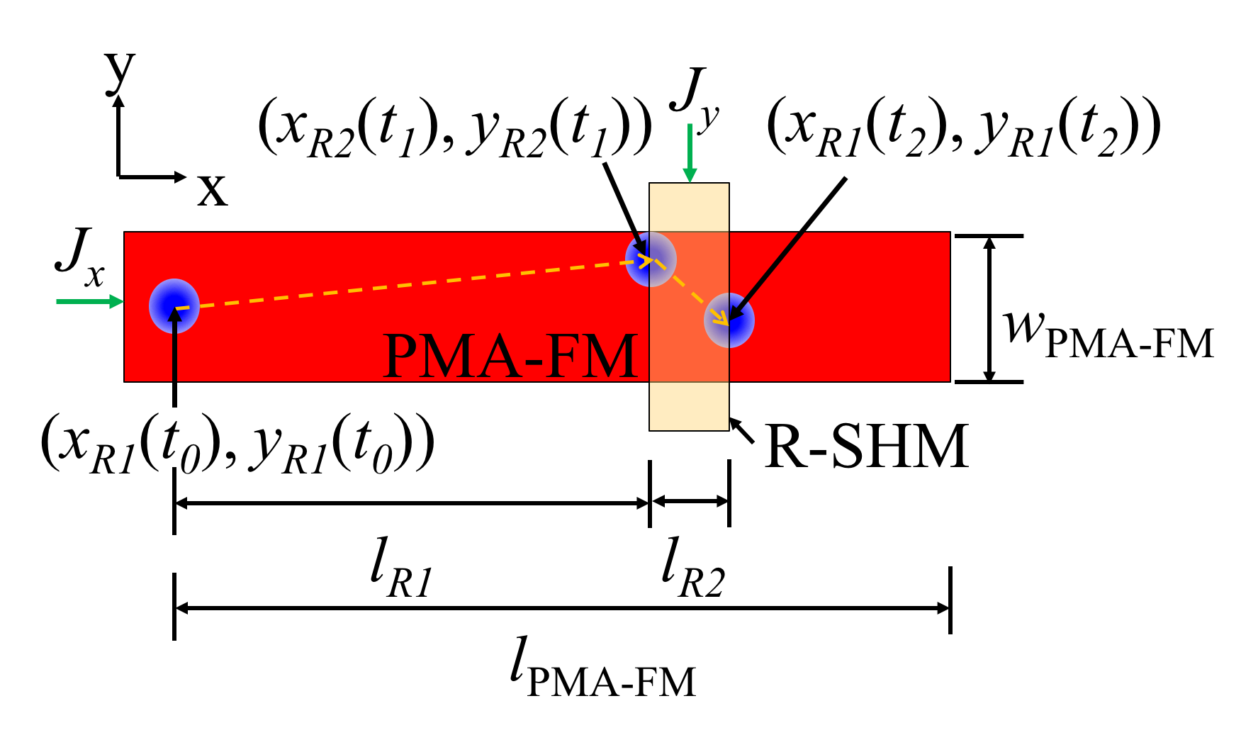
When is applied to the SHM, as shown in Fig. 2(a), the transverse motion of the skyrmion causes it to travel towards the edge of the PMA–FM where it is annihilated. The placement of R–SHM above the PMA–FM addresses this issue. As shown in Fig. 2(b), we assume equally-spaced repeaters above the PMA–FM, and define segments of the PMA–FM that do not lie under R–SHM as Region 1 (), with length . The segments of the PMA–FM below R–SHM is denoted as Region 2 (), with length . The width of the PMA–FM is denoted as .
The role of the repeater is to deflect the skyrmion back into the body of the PMA–FM, and is chosen to ensure the deviation due to the Magnus force does not allow the skyrmion to reach the PMA–FM edge where it would be annihilated. The transistor is turned on by applying a gate voltage and a charge current with density is applied through the R–SHM layer in a direction transverse to that of , as shown in Fig. 2(b). Therefore in , the skyrmion motion is defined by the forcing function from and in , the skyrmion motion is dictated by the forcing function from both and . Due to , the skyrmion experiences a longitudinal motion in the y–direction and a Magnus force in the x–direction. The magnitudes of and can be optimized such that the skyrmion moves back towards the PMA–FM interior from its edge to negate the y–direction shift due to the Magnus force from . At the same time, the Magnus force due to moves the skyrmion forward towards the output.
Additional repeaters can be inserted along the PMA–FM length to allow the skyrmion to traverse long interconnects. Our approach with repeaters differs from conventional approaches [10, 21, 20, 13, 18] that only use applied at one end of the SHM to propagate the skyrmion in the PMA–FM. In these approaches, a low current density is essential to contain the skyrmion within the PMA–FM, directly translating to high skyrmion propagation delays. In contrast, our novel approach of inserting R–SHM and using both and allows the use of high current densities for fast propagation of skyrmions through the PMA–FM, while ensuring that the skyrmion is not annihilated due to its transverse motion.
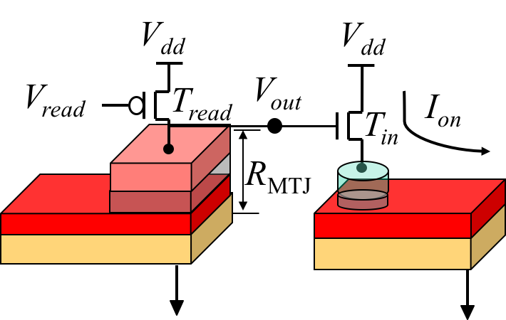
Stage 3 – Skyrmion detection: Once the skyrmion reaches the output end, it creates a polarization in the free layer of the MTJ stack at the output. The Pin–FM magnetization is anti-parallel to that of the steady-state PMA–FM. The presence or absence of a skyrmion is differentiated by different resistances for the MTJ stack for these two cases [5, 14]: the resistance is high if no skyrmion is present, and low otherwise. The time required for the skyrmion detection is denoted by .
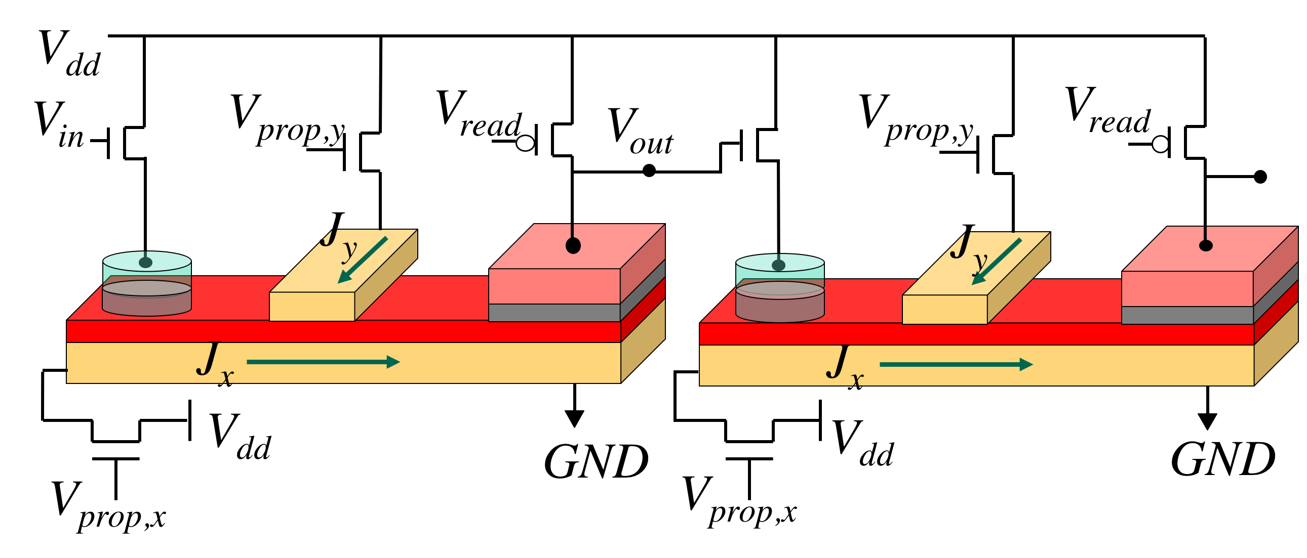
Stage 4 – Cascading logic stages: The cascading of successive SkyLogic stages can be achieved as shown in Fig. 3. The voltage is set to low to turn on the transistor and a voltage is induced at the output node. This switches the transistor in the next logic stage on. The current density through is greater than the critical nucleation current density, , when the skyrmion is absent at the output end in the PMA–FM layer of the MTJ. Therefore, a skyrmion is nucleated; when the current density is lower than the critical value, the skyrmion is present at the output, and no nucleation occurs at the next stage. Thus, we realize an inverter.
II-B Design of the SkyLogic NOR gate
The presence of a skyrmion in at least one of the input results in a skyrmion being absent (present) at the output to realize a (N)OR gate. Skyrmion-based (N)OR gates has been shown in [24]. We use this design and combine it with that of the SkyLogic inverter presented in Section II-A to build a NOR gate, as shown in Fig. 4. For clarity, we do not show the CMOS transistors.
The SkyLogic NOR2 gate consists of two input branches and an output branch. For each of the two inputs, when a current with density is applied, a skyrmion is nucleated if , thereby representing logic 1. The absence of a skyrmion, when , represents logic 0. A charge current with density sent through the SHM through each of the input branches propagates the skyrmion from the input branch towards the output branch of the PMA–FM. As in the case of the SkyLogic inverter, R–SHMs are inserted in the input branches atop the PMA–FM to correct the course of the skyrmion. At the output end, if any one of the inputs is logic 1, i.e., if at least one skyrmion is nucleated at the input end, then a skyrmion is present at the output end. The skyrmion is then detected using the MTJ stack, as explained in Stage 3 of Section II-A. The voltage at the output node, , therefore represents a logical NOR of the two inputs.
III Performance modeling of SkyLogic inverter
In this section, we analyze the performance of SkyLogic inverter shown in Fig. 1 in the four stages of its operation.
III-A Skyrmion nucleation
We model the skyrmion nucleation using the micromagnetic simulator OOMMF [12] with the DMI extension [17]. The PMA–FM is initially uniformly magnetized in the z direction. A spin-polarized current is sent through the P–FM in the z direction. If the current density through the P–FM, , is greater than , then a skyrmion is nucleated in the PMA–FM layer beneath the P–FM.
III-B Skyrmion propagation
Next, we separately analyze the propagation of the skyrmion in regions and using Fig. 2(b).
Case 1: Skyrmion propagation in : The motion of the skyrmion in can be explained using the two-dimensional Thiele equation [2, 13, 20, 21, 10] as follows:
| (1) |
where is the gyrovector, is the PMA–FM saturation magnetization, is the PMA–FM thickness, is the gyromagnetic ratio, / is the skyrmion chirality, and is the confinement constant. The skyrmion velocity in is denoted by its x– and y– components as . The time-dependent x– (y–) position of the skyrmion center in of the PMA–FM is given by (). The skyrmion driving force due to the SHE as a result of , is given by . The damping constant is denoted by while the dissipative force tensor is given by . The skyrmion radius is given by , denotes its domain-wall width and represents the spin Hall angle. The repelling force experienced by the skyrmion from the PMA–FM edges along its width is given by .
The first term in Equation (1), , represents the impact of the Magnus force on the skyrmion, and defines its transverse motion. The second term in Equation (1), , is the opposing force experienced by the skyrmion due to the intrinsic damping of the PMA–FM. At steady state, these forces are countered by the driving force due to SHE, , and the repelling force, . We solve the 2D first-order differential equation (1) to obtain and :
| (2) | ||||
| (3) |
where is the characteristic relaxation time of the skyrmion. At time , (x,y) co-ordinates of the center of the nucleated skyrmion is given by (,). The term represents the ratio of the Magnus force and dissipative force. The relative magnitude of each of these forces determines the net strength of the opposing force to the skyrmion propagation. The term does not have an counterpart because there is no repelling force on the skyrmion from the PMA–FM edges along its length.
Case 2: Skyrmion propagation in : We modify Equation (1) to model the skyrmion motion in , in which both and are active, by adding to the right hand side. Here, is the force experienced by the skyrmion as a result of the SHE arising from in Region 2. The instantaneous skyrmion velocity in is given by with () denoting the time-dependent x–position (y–position) of the center of the skyrmion in . We solve the 2D first-order differential equation for to obtain and :
| (4) | ||||
| (5) |
At time , the skyrmion reaches the PMA–FM edge in and a current is applied along R-SHM length as shown in Fig. 2(b). The (x,y) coordinates of the skyrmion center at time is given by (, ). Equation (4) shows that the skyrmion is propelled forward towards the PMA–FM output in by the combined force of and the Magnus force resulting from applying in R-SHM. The value of in should be chosen such that the skyrmion continues to move back towards the PMA–FM interior upon its application. This can be achieved by enforcing the constraint and in Equations (4) and (5).
For a fixed PMA–FM length, the number of required R-SHMs, , depend on the choice of and and can be determined by solving the skyrmion displacement equations for each of and regions independently. The average net velocity (propagation time) of the skyrmion, (), as it propagates from the PMA–FM input to its output with repeaters, is therefore given by the sum of their velocities (propagation times) in and .

III-C Skyrmion detection and cascading SkyLogic devices
We explain the detection of the skyrmion using the MTJ stack. The initial magnetization in the Pin–FM layer is uniform in direction, whereas that of the PMA–FM layer is in the z direction. Let () denote the resistance of the MTJ stack when the skyrmion is absent (present) in the PMA–FM layer, which forms the free layer of the MTJ stack. We can write and as
| (6) |
Here, () corresponds to the resistance of the MTJ stack when its pinned layer and the free layer are parallel (anti-parallel) to each other. In the absence of the skyrmion (logic 0) in the PMA–FM layer, corresponds to . However, when the skyrmion is present in the PMA–FM layer (logic 1), the PMA–FM layer magnetization is not completely parallel to the pinned layer due to the averaging nature of the magnetization profile of the skyrmion [22, 26, 23]. We therefore model as a linear combination of and with being the scalar coefficient defined as . Here refers to the area of the skyrmion while refers to the area of the detector enclosed by the length of the fixed layer of the MTJ, , and its width, . Since , it follows that .
We analyze the cascading of two SkyLogic devices, shown in Fig. 5(a), with the equivalent circuit shown in Fig. 5(b). The voltage at the output node, is determined by the voltage divider circuit formed by the resistances of transistor (), MTJ (), and SHM (). Once the transistor is turned on, the current in the transistor in the next SkyLogic stage, , is proportional to and its strength determines whether a skyrmion is nucleated at the next stage.
III-D Modeling performance
Here, we outline the model used to measure the performance of SkyLogic inverter. We model the delay, , and energy, , of the SkyLogic inverter in Fig. 1 as follows.
| (7) | ||||
The energy dissipated during the nucleation, propagation, detection, and peripheral CMOS transistor switching is given respectively by , , , and . The energy terms and represent the Joule heating during the nucleation and detection process, while represents both Joule heating due to and , and the energy required to turn on the CMOS transistors that supply both and . The energy required to turn on the rest of the CMOS transistors is grouped in the term .
| Parameter | Value |
|---|---|
| [nm3] | 200500.4 |
| [nm3] | 200501 |
| [nm3] | 25501 |
| Exchange constant, [pJ/m] | 15 |
| Radius of the skyrmion, [m] | |
| Confinement constant, [N/m] | |
| , [-m] | |
| [-m] | |
| Spin Hall angle, | 0.33 |
| Spin polarization, | 1 |
| TMR of the output MTJ stack [] | 300 |
| [] | 4000 |
| 0.5 | |
| CMOS transistor gate capacitance, [F] | |
| , [V] | 1 |
| , [V] | 0.25 |
IV Results and Discussion
In this section, we demonstrate the SkyLogic device design and obtain its delay and energy with the help of the models explained in Section III and the peripheral CMOS circuity implemented in the 10nm Predictive Technology Model (PTM) [1] with the parameters shown in Table I.
IV-A Insertion of R–SHM
Here, we examine the process of R–SHM insertion in a SkyLogic device. We use the following PMA–FM material parameters in our simulations: A/m, J/m3, . We show, at the end of Section IV-B, that this design point gives the best energy-delay product for skyrmion propagation phase. We assume that the center of the nucleated skyrmion is the origin of the coordinate system. For various values of , we simulate the skyrmion trajectory by solving the displacement equations shown in Section III-B and plot the results in Fig. 6(a).
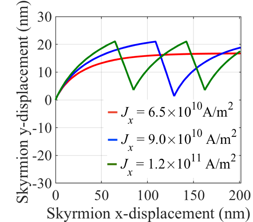
For A/m2, the skyrmion reaches the PMA–FM output without reaching the edge due to low transverse and longitudinal velocity. Next, when is increased to A/m2, is greater than and therefore reaches the PMA–FM edge faster than the case where A/m2. In this case, an R–SHM needs to be inserted to avoid the skyrmion being annihilated at the edge. When an R–SHM is inserted and A/m2 is applied through it, the skyrmion is pushed back into the interior of the PMA–FM in underneath the R–SHM. When is further increased to A/m2, further increases relative to increase in and causes the skyrmion to reach the PMA–FM edge faster than the earlier two cases. Two R–SHMs are required in this case between the PMA–FM input and output.
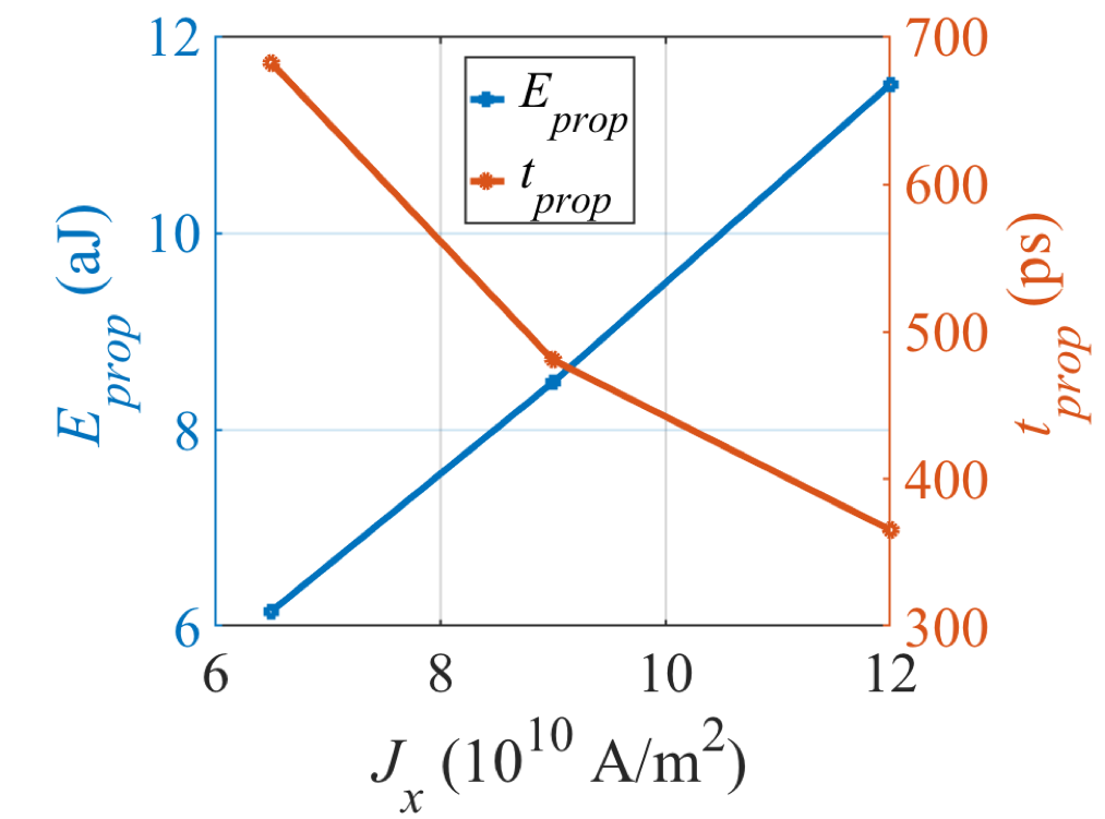
Next, we calculate the cost of inserting an R–SHM on and and plot the results in Fig. 6(b). As increases, decreases because of an increase in and also due to the effect of the Magnus force in along the x–direction due to which propels the skyrmion faster towards the output. The propagation energy, , however increases. Though is directly proportional to , the R–SHM insertion requires an additional transistor to drive through it, thereby increasing . The net energy-delay product, , as is increased from A/m2 to A/m2, decreases because of the decrease in . With a further increase in to A/m2, decreases, but increases due to Joule heating from the currents and in SHM and R–SHM, respectively, and the energy required to turn two transistors on. The decrease in is outweighed by the increase in and therefore increases. Therefore, inserting one R–SHM provides an optimal for this design point for the chosen values of and .
IV-B Skyrmion propagation
The initial steady-state magnetization of the PMA–FM is set to z direction. We evaluate and at the design points formed by the combination of the following material parameters and their values: { A/m, A/m, A/m, A/m , A/m}, { J/m3, J/m3, J/m3}, {0.05, 0.1, 0.15, 0.2, 0.25}. At these design points, we assume that a skyrmion can be nucleated at the input end of the PMA–FM by injecting a spin polarized current through P–FM. We study the impact of these parameters on the skyrmion velocity, device energy, and energy-delay product (EDP).
Skyrmion velocity, device energy, and EDP: We choose A/m2 such that we obtain ps. We fix the value of A/m2. This choice of ensures that we obtain a valid skyrmion trajectory in and for each design point. We set , i.e., we restrict the number of R–SHMs that can be inserted to two and disregard the material parameters that violate this criteria. A large number of R–SHMs is impractical because additional R–SHMs would incur extra energy to route through the addition of access transistors leading to higher as we observed in Section IV-A. We also disregard material parameters where it is impractical to insert a R–SHM in cases where it would physically overlap with the MTJ structure. We show and as a function of the three material parameters in Figs. 7(a) and 7(b), respectively. In these plots, we denote the infeasible design points by black triangles.
Impact of and : For , the skyrmion reaches the PMA–FM edge along its width faster. This is because for low values of , we have and , the skyrmion experiences lower opposition to motion and requires more than two R–SHMs, as indicated by the black triangles in Fig. 7(a). For and J/m3, the skyrmion trajectory is such that it is infeasible to insert an R–SHM. Therefore, we discard these design points. In general, for a chosen value of and , increasing decreases , and therefore increases as shown in Fig. 7(a). The energy-delay product, , shows a corresponding increase, as seen from Fig. 7(b), because is directly proportional to . Hereafter, we restrict our analysis to feasible design points that are represented by circles in Figs. 7(a) and 7(b).
As increases, the domain-wall width, , decreases by . Since the dissipative tensor, , is inversely proportional to , it follows that increasing will increase . As the term determines the strength of the opposition to the skyrmion propagation, increasing has the same effect as increasing .
Impact of : As increases, for a given and , decreases as seen in Fig. 7(a). The dependence of the and skyrmion displacement equations (2) and (4) on can be seen in the term . Simplifying , we determine that is directly proportional to . Therefore, for larger , the skyrmion takes longer to reach the PMA–FM output because of the larger relaxation time, thereby reducing . The propagation energy, , which is directly proportional to also increases with increase in , for a given . This in turn results in an increase in as seen from Fig. 7(b).
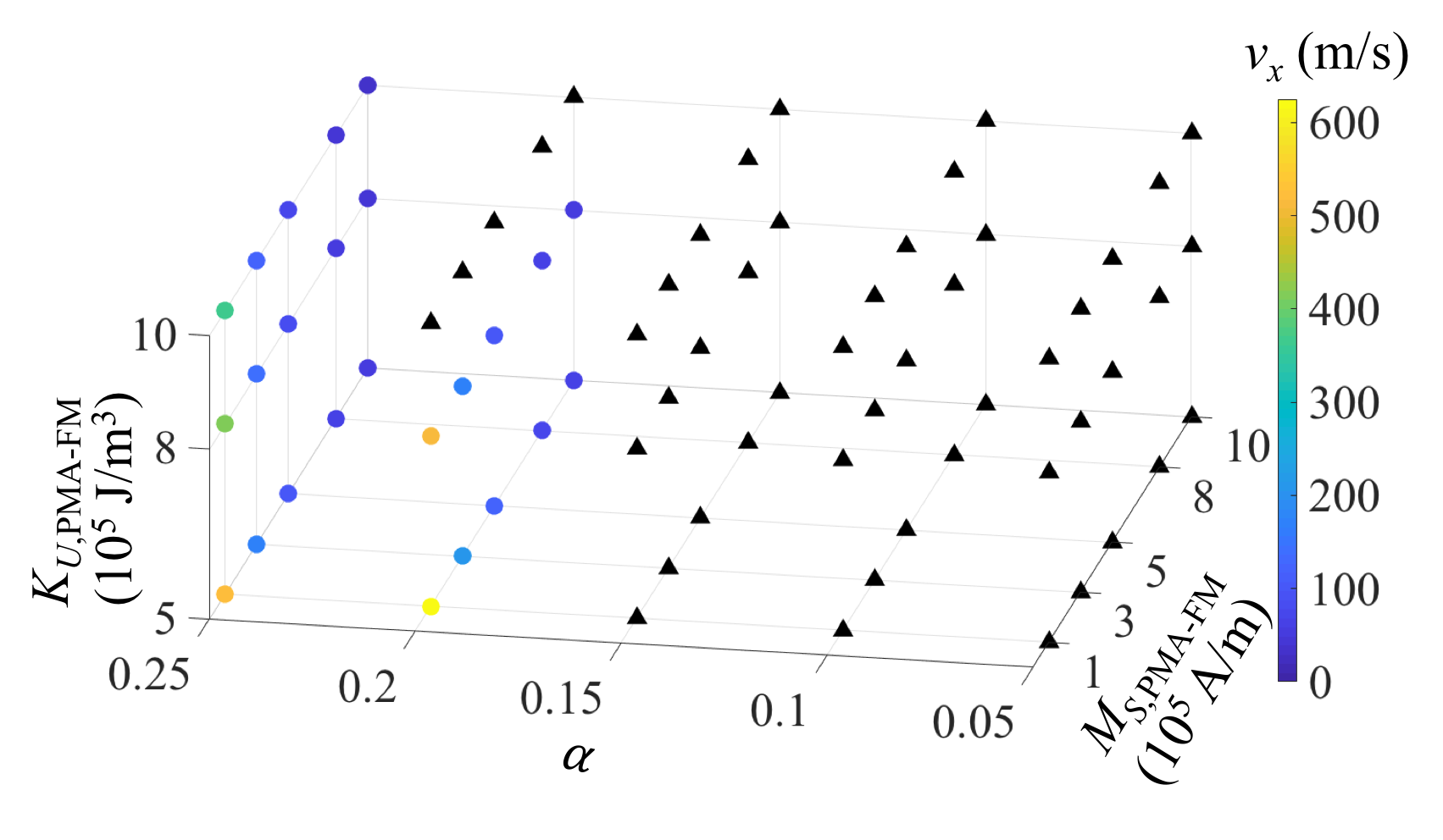
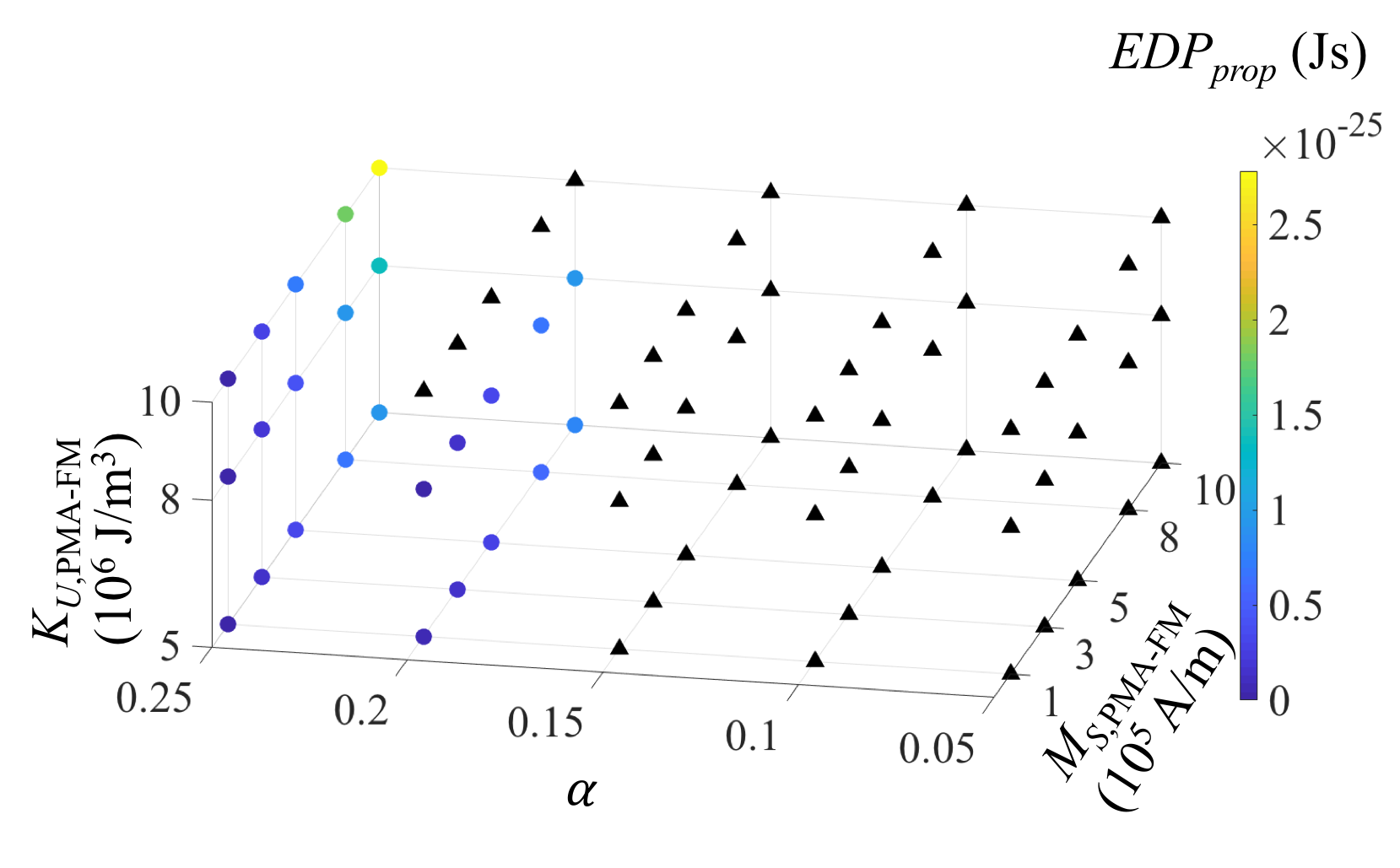
With this experiment, we obtain the design point that provides the best as: A/m, J/m3, and . At this design point, we have m/s, ps, aJ, , and Js.
IV-C Skyrmion nucleation
The critical current density required for skyrmion nucleation primarily depends on the choice of [10]. A smaller (larger) value of results in lower (higher) critical current density. However, as seen in Section IV-B, the choice of and , are infeasible for skyrmion propagation. Therefore, we restrict the design space exploration of our nucleation process to feasible design points for skyrmion propagation. We perform our nucleation experiment in OOMMF and observe that once , the skyrmion nucleates within ps.
In order to derive PMA–FM material parameters that provides the best performance, we choose the design point that provides the minimum energy-delay product for both the nucleation and the propagation. This design point is obtained as: A/m, J/m3, and . At this point, for propagation we obtain m/s, ps, aJ, and Js. For nucleation, the parameter values are as follows: A ( A/m2), ps, fJ, and Js.
IV-D Skyrmion detection and logic cascading
We analyze the skyrmion detection and cascading of two SkyLogic devices using the circuit shown in Fig. 5(b). We perform the circuit simulation in SPICE with the parameters shown in Table I. When is turned on by applying V, the voltage at the output node is given by V (V) when (). Correspondingly, the next stage transistor on current is given by A (A). We observe that A, corresponding to A/m2, can nucleate a skyrmion in the next stage. This can be seen from the OOMMF simulation results shown in Section IV-C. In the case of A, the charge current is insufficient for skyrmion nucleation. The circuit simulation is run for a period of ps, the time required to nucleate a skyrmion in the next stage. From the simulation, we determine, fJ and Js.
IV-E Total delay and energy of the SkyLogic device
With the parameters shown in Table I, we obtain fJ. Using Equation (7), we obtain ps and fJ. The total energy-delay product of the SkyLogic device is given by Js. We note that for an optimized SkyLogic inverter, as seen from Section IV-C, skyrmion nucleation is an energy-expensive process. This is due to the high current density required to nucleate the skyrmion. The detection process, similarly also requires a high current through the MTJ read stack, and therefore consumes a large amount of energy.
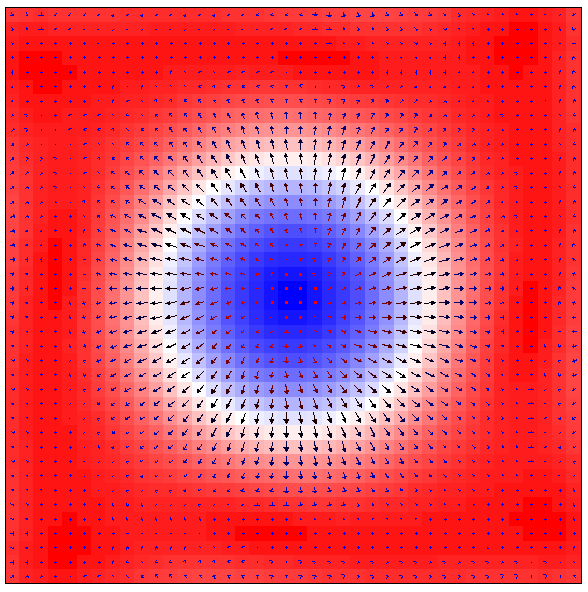
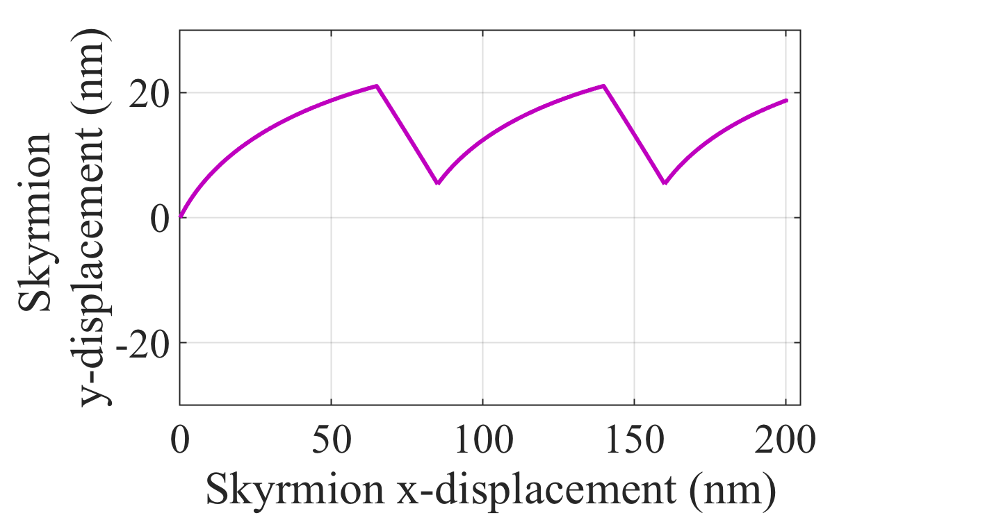
We show the result of the skyrmion nucleation for the optimal design point in Fig. 8(a). The skyrmion trajectory in the PMA–FM during the skyrmion propagation process for this design point is shown in Fig. 8(b). We assume that the skyrmion nucleation process nucleates the skyrmion in the PMA–FM at (x,y) coordinate of the skyrmion center corresponding to (nm, nm). It is then propagated to the output end of the PMA–FM such that its final (x,y) coordinate corresponds to (nm, nm). Along with the longitudinal motion, the transverse motion of the skyrmion in and its subsequent motion into the interior of the PMA–FM in can be clearly deduced from Fig. 8(b). At the optimal design point, we need two R–SHMs to be inserted to avoid the skyrmion being destroyed at the edge of the PMA–FM.
V Conclusion
In this paper, we present SkyLogic, a proposal for a skyrmion-based logic device. We present a framework for analyzing the device performance by analyzing the skyrmion nucleation in a PMA–FM using micromagnetic simulation, analyzing the skyrmion propagation in the PMA–FM using an analytical model, and analyzing the skyrmion detection at the output using an MTJ stack. The transverse motion of skyrmion due to Magnus force during the current-driven skyrmion propagation restricts the use of high current densities and leads to high propagation latencies. We present a novel circuit-based technique to counter the Magnus force and allows the use of high current densities to drive the skyrmion from the SkyLogic input to the output. We also perform a complete design space exploration of the device for nucleation and propagation over a range of PMA–FM material parameters and obtain an optimal design point for the SkyLogic inverter. At this design point, we evaluate the performance of the SkyLogic inverter and obtain a delay of ps and an energy of fJ.
References
- [1] “Predictive Technology Model,” http://ptm.asu.edu, accessed: 2016-08-09.
- [2] A. A. Thiele, “Steady–state motion of magnetic domains,” Physical Review Letters, vol. 30, pp. 230–233, Feb. 1973, doi:10.1103/PhysRevLett.30.230.
- [3] A. Fert, N. Reyren, and V. Cros, “Magnetic skyrmions: advances in physics and potential applications,” Nature Reviews Materials, vol. 2, no. 17031, pp. 1–15, June 2017, doi:10.1038/natrevmats.2017.31.
- [4] A. Fert, V. Cros, and J. Sampaio, “Skyrmions on the track,” Nature Nanotechnology, vol. 8, no. 3, pp. 152–156, Mar. 2013, doi:10.1038/nano.2013.29.
- [5] C. Hanneken, F. Otte, A. Kubetzka, B. Dupé, N. Romming, K. Von Bergmann, R. Wiesendanger, and S. Heinze, “Electrical detection of magnetic skyrmions by tunnelling non-collinear magnetoresistance,” Nature Nanotechnology, vol. 10, no. 12, pp. 1039–1042, Oct. 2015, doi:10.1038/nnano.2015.218.
- [6] C. Pan and A. Naeemi, “An expanded benchmarking of beyond–CMOS devices based on Boolean and neuromorphic representative circuits,” IEEE Journal on Exploratory Solid–State Computational Devices and Circuits, vol. 3, pp. 101–110, Dec. 2017, doi:10.1109/JXCDC.2018.2793536.
- [7] D. A. Allwood, G. Xiong, C. C. Faulkner, D. Atkinson, D. Petit, and R. P. Cowburn, “Magnetic domain-wall logic,” Science, vol. 309, no. 5741, pp. 1688–1692, Sep. 2005, doi:10.1126/science.1108813.
- [8] D. E. Nikonov, G. I. Bourianoff, and T. Ghani, “Proposal of a spin torque majority gate logic,” IEEE Electron Device Letters, vol. 32, no. 8, pp. 1128–1130, Aug. 2011, 10.1109/LED.2011.2156379.
- [9] D. E. Nikonov and I. A. Young, “Benchmarking of beyond–CMOS exploratory devices for logic integrated circuits,” IEEE Journal on Exploratory Solid–State Computational Devices and Circuits, vol. 1, pp. 3–11, Dec. 2015, doi:10.1109/JXCDC.2015.2418033.
- [10] J. Sampaio, V. Cros, S. Rohart, A. Thiaville, and A. Fert, “Nucleation, stability and current–induced motion of isolated magnetic skyrmions in nanostructures,” Nature Nanotechnology, vol. 8, no. 11, pp. 839–844, Oct. 2013, doi:10.1038/nnano.2013.210.
- [11] M. G. Mankalale, Z. Liang, Z. Zhao, C. H. Kim, J. P. Wang, and S. S. Sapatnekar, “CoMET: Composite-input magnetoelectric-based logic technology,” IEEE Journal on Exploratory Solid–State Computational Devices and Circuits, vol. 3, pp. 27–36, Apr. 2017, doi:10.1109/JXCDC.2017.2690629.
- [12] M. J. Donahue and D. G. Porter, OOMMF User’s Guide. US Department of Commerce, Technology Administration, National Institute of Standards and Technology, Gaithersburg, Maryland, USA, 1999.
- [13] R. Tomasello, E. Martinez, R. Zivieri, L. Torres, M. Carpentieri, and G. Finocchio, “A strategy for the design of skyrmion racetrack memories,” Scientific Reports, vol. 4, no. 6784, pp. 1–6, Oct. 2014, doi:10.1038/srep06784.
- [14] R. Tomasello, M. Ricci, P. Burrascano, V. Puliafito, M. Carpentieri, and G. Finocchio, “Electrical detection of single magnetic skyrmion at room temperature,” AIP Advances, vol. 7, no. 5, pp. 056 022–1–056 022–8, Feb. 2017, doi:10.1063/1.4975998.
- [15] S. Luo, M. Song, X. Li, Y. Zhang, J. Hong, X. Yang, X. Zou, N. Xu, and L. You, “Reconfigurable Skyrmion Logic Gates,” Nano Letters, vol. 18, no. 2, pp. 1180–1184, Jan. 2018, doi:10.1021/acs.nanolett.7b04722.
- [16] S. Pizzini, V. Uhlíř, J. Vogel, N. Rougemaille, S. Laribi, V. Cros, E. Jiménez, J. Camarero, C. Tieg, E. Bonet, M. Bonfim, R. Mattana, C. Deranlot, F. Petroff, C. Ulysse, G. Faini, and A. Fert, “High domain wall velocity at zero magnetic field induced by low current densities in spin valve nanostripes,” Applied Physics Express, vol. 2, no. 2, pp. 023 003–1–023 003–3, Jan. 2009, doi:10.1143/APEX.2.023003.
- [17] S. Rohart and A. Thiaville, “Skyrmion confinement in ultrathin film nanostructures in the presence of Dzyaloshinskii-Moriya interaction,” Physical Review B, vol. 88, no. 18, pp. 184 422–1–184 422–8, Nov. 2013, doi:10.1103/PhysRevB.88.184422.
- [18] S. Woo, K. M. Song, H.-S. Han, M.-S. Jung, M.-Y. Im, K.-S. Lee, K. S. Song, P. Fischer, J.-I. Hong, J. W. Choi, B. C. Mjin, C. K. Hyun, and J. Chang, “Spin-orbit torque-driven skyrmion dynamics revealed by time-resolved X-ray microscopy,” Nature Communications, vol. 8, pp. 15 573–1–15 573–8, May 2017, doi: 10.1038/ncomms15573.
- [19] S. Woo, K. M. Song, X. Zhang, Y. Zhou, M. Ezawa, X. Liu, S. Finizio, J. Raabe, N. J. Lee, S.-I. Kim, S.-Y. Park, Y. Kim, J.-Y. Kim, D. Lee, O. Lee, J. W. Choi, B.-C. Min, H. C. Koo, and J. Chang, “Current-driven dynamics and inhibition of the skyrmion Hall effect of ferrimagnetic skyrmions in GdFeCo films,” Nature Communications, vol. 9, no. 959, pp. 1–8, Mar. 2018, doi:10.1038/s41467-018-03378-7.
- [20] V. Raposo, R. F. L. Martinez, and E. Martinez, “Current–driven skyrmion motion along disordered magnetic tracks,” AIP Advances, vol. 7, no. 5, pp. 056 017–1–056 017–7, Feb. 2017, doi:10.1063/1.4975658.
- [21] W. Jiang, X. Zhang, G. Yu, W. Zhang, X. Wang, M. B. Jungfleisch, J. E. Pearson, X. Cheng, O. Heinonen, K. L. Wang, Y. Zhou, A. Hoffmann, and S. G. E. Velthuis, “Direct observation of the skyrmion Hall effect,” Nature Physics, vol. 13, no. 2, pp. 162–169, Sep. 2017, doi:10.1038/nphys3883.
- [22] W. Kang, Y. Huang, C. Zheng, W. Lv, N. Lei, Y. Zhang, X. Zhang, Y. Zhou, and W. Zhao, “Voltage controlled magnetic skyrmion motion for racetrack memory,” Scientific Reports, vol. 6, no. 23164, pp. 1–11, Mar. 2016, doi: 10.1038/srep23164.
- [23] W. Kang, Y. Huang, X. Zhang, Y. Zhou, and W. Zhao, “Skyrmion–Electronics: An Overview and Outlook,” Proceedings of the IEEE, vol. 104, no. 10, pp. 2040–2061, Oct. 2016, doi:10.1109/JPROC.2016.2591578.
- [24] X. Zhang, M. Ezawa, and Y. Zhou, “Magnetic skyrmion logic gates: conversion, duplication and merging of skyrmions,” Scientific Reports, vol. 5, no. 9400, pp. 1–8, Mar. 2015, doi:10.1038/srep09400.
- [25] X. Zhang, Y. Zhou, and M. Ezawa, “Magnetic bilayer-skyrmions without skyrmion Hall effect,” Nature Communications, vol. 7, no. 10293, pp. 1–7, Jan. 2016, doi: 10.1038/ncomms10293.
- [26] X. Zhang, Y. Zhou, M. Ezawa, G. P. Zhao, and W. Zhao, “Magnetic skyrmion transistor: skyrmion motion in a voltage-gated nanotrack,” Scientific Reports, vol. 5, no. 11369, pp. 1–8, June 2015, doi:10.1038/srep11369.
![[Uncaptioned image]](/html/1811.02016/assets/bib_pics/MMG.jpg) |
Meghna G. Mankalale received the B.E. degree from Visvesvaraya Technological University, India in 2007. She worked as a Research and Development Engineer in the Electronic Design Automation group in IBM, India from 2007 to 2013. She is currently pursuing the Ph.D. degree in the Department of Electrical and Computer Engineering at the University of Minnesota. Her research interests include design and optimization techniques for beyond-CMOS technologies. |
![[Uncaptioned image]](/html/1811.02016/assets/bib_pics/Zhengyang.jpg) |
Zhengyang Zhao is currently pursuing the Ph.D. degree in Electrical and Computer Engineering at the University of Minnesota, Minneapolis, MN. He received the B.S. degree in Electrical Engineering from Xi’an Jiaotong University, China. His research focuses on the development of novel spintronic devices to implement energy-efficient memory cells and logic applications. His recent work includes studying current-induced magnet reversal using spin-orbit torque (SOT), as well as voltage-induced magnet reversal using piezoelectric strain or VCMA effect. More specific work includes the stack design, MTJ cell nanofabrication, advanced device characterization and physics study. |
![[Uncaptioned image]](/html/1811.02016/assets/bib_pics/Wang.jpg) |
Jian-Ping Wang received the Ph.D. degree from the Institute of Physics, Chinese Academy of Sciences, where he performed research on nanomagnetism, Beijing, China, in 1995. He was a Post-Doctoral Researcher with the National University of Singapore, Singapore, from 1995 to 1996. He established and managed the Magnetic Media and Materials Program with the Data Storage Institute, Singapore, from 1998 to 2002. He joined the faculty of the Electrical and Computer Engineering Department with the University of Minnesota, Minneapolis, MN, USA, in 2002 and was promoted to Full Professor in 2009. He is the Robert F. Hartmann Chair and a Distinguished McKnight University Professor of Electrical and Computer Engineering and a member of the Graduate Faculty in Physics and Chemical Engineering and Materials Science at the University of Minnesota. He is the Director of the Center for Spintronic Materials, Interfaces and Novel Architectures (C-SPIN), one of six STARnet program centers. Dr. Wang received the Information Storage Industry Consortium Technical Award in 2006 for his pioneering experimental work in exchange coupled composite magnetic media and the Outstanding Professor Award for his contribution to undergraduate teaching in 2010. His group is also known for several important experimental demonstrations and conceptual proposals, including the perpendicular spin transfer torque device, the magnetic tunnel junction-based logic device and random number generator, ultrafast switching of thermally stable MTJs, topological insulator spin pumping at room temperature, and a computation architecture in random access memory. |
![[Uncaptioned image]](/html/1811.02016/assets/bib_pics/sachin.jpg) |
Sachin S. Sapatnekar (S’86, M’93, F’03) received the B. Tech. degree from the Indian Institute of Technology, Bombay, the M.S. degree from Syracuse University, and the Ph.D. degree from the University of Illinois. He taught at Iowa State University from 1992 to 1997 and has been at the University of Minnesota since 1997, where he holds the Distinguished McKnight University Professorship and the Robert and Marjorie Henle Chair in the Department of Electrical and Computer Engineering. He has received seven conference Best Paper awards, a Best Poster Award, two ICCAD 10-year Retrospective Most Influential Paper Awards, the SRC Technical Excellence award and the SIA University Researcher Award. He is a Fellow of the ACM and the IEEE. |