Open-Circuit Voltage Deficit in Cu2ZnSnS4 Solar Cells by Interface Band Gap Narrowing
Abstract
There is evidence that interface recombination in Cu2ZnSnS4 solar cells contributes to the open-circuit voltage deficit. Our hybrid density functional theory calculations suggest that electron-hole recombination at the Cu2ZnSnS4/CdS interface is caused by a deeper conduction band that slows electron extraction. In contrast, the bandgap is not narrowed for the Cu2ZnSnSe4/CdS interface, consistent with a lower open-circuit voltage deficit.
Solar cells based on earth-abundant Cu2ZnSn(S,Se)4 (CZTSSe) absorber materials suffer from lower solar conversion efficiency than other mature technologies because of the large open-circuit voltage (VOC) deficit.Polizzotti et al. (2013); Walsh et al. (2012); Yang et al. (2016); Guchhait et al. (2016); Bourdais et al. (2016); Grenet et al. (2018); Yan et al. (2018) Since the open-circuit voltage is determined by the quasi-Fermi level splitting, understanding recombination mechanisms not only in the bulk regionKim et al. (2018) but also at the interfacesGunawan et al. (2010); Wang et al. (2014); Crovetto et al. (2017); Redinger and Unold (2018) is essential to developing a proper passivation strategy to achieve a higher efficiency.Repins et al. (2015) In this circumstance, fundamental properties of interfaces formed in CZTSSe solar cells need to be thoroughly investigated,Crovetto and Hansen (2017); Kaur et al. (2017); Antunez et al. (2017); Turnbull et al. (2018) a strategy that has proved effective in other mature technologies.Aberle (2000); Battaglia et al. (2016); Park et al. (2018a)
One open question in this community is why there is stronger interface recombination in CZTSSe solar cells with a higher S composition ratio. This increased recombination is primarily characterized by a smaller activation energy for recombination compared with the bandgap energy.Wang et al. (2010); Redinger et al. (2013); Yan et al. (2018) Previously, a cliff-type conduction band offset (CBO)Crovetto and Hansen (2017) has been suggested to be the culprit behind this stronger interface recombination.Wang et al. (2010) However, a recent study indicated that the CBO is instead actually a weak spike under the strain-free condition when temperature effects were considered.Monserrat et al. (2018)
Another recent model based on density functional theory (DFT) calculations insists that Cu-S bonds at the CZTS/CdS interface can introduce gap states 0.20.3 eV higher than the VBM even without point defects.Crovetto et al. (2017) Performing device simulations taking into account the interface states, the study was able to reproduce the experimentally measured temperature dependent VOC data without cliff-type conduction band offsets.Crovetto et al. (2017, 2018) Since the electronic band gap of semiconductors is usually underestimated in the generalized gradient approximation (GGA) calculations,Heyd et al. (2005) the Hubbard U correction, which has been widely used to improve the band gap and formation enthalpies,Wang et al. (2006); Jain et al. (2011); Noh et al. (2011) was applied in the study.Crovetto et al. (2017) The results are worth being re-examined by more advanced methods, considering the importance and implications of the conclusion.
In this letter, we report our first-principles DFT calculation results on the electronic structure of CZTS(Se)/CdS interface. Several exchange-correlation functionals were examined to check how the interface band gap is narrowed. We suggest that the interface band gap narrowing is caused by the lowered conduction band of CZTS. As the electron carriers are captured at the interface, the quasi-Fermi level splitting and the open-circuit voltage will be reduced significantly.
In our DFT calculations, we used the projector augmented wave (PAW) method to describe the interaction between ions and electrons,Blöchl (1994) as implemented in the Vienna ab-initio Simulation Package (VASP) code.Kresse and Furthmüller (1996) To verify the effect of exchange-correlation functional on the electronic structure of materials, we employed various exchange-correlation functional including PBE,Perdew et al. (1996) revised PBE,Zhang and Yang (1998) PBEsol,Perdew et al. (2008) AM05,Armiento and Mattsson (2005) SCAN,Sun et al. (2015) and HSE06.Heyd et al. (2003) The wavefunctions were expanded in plane waves with an energy cutoff of 400 eV. A 666 k-point grid was used for Brillouin zone integration of the primitive cell. Here we consider zinc-blende CdS (zb-CdS), not thermodynamically stable wurtzite CdS (wz-CdS) to avoid the effect of spontaneous polarization in the interface calculations. Following our examination of the pristine interfaces, further work is needed to consider the role of defects and non-stoichiometry on the interfacial processes in kesterite solar cells.
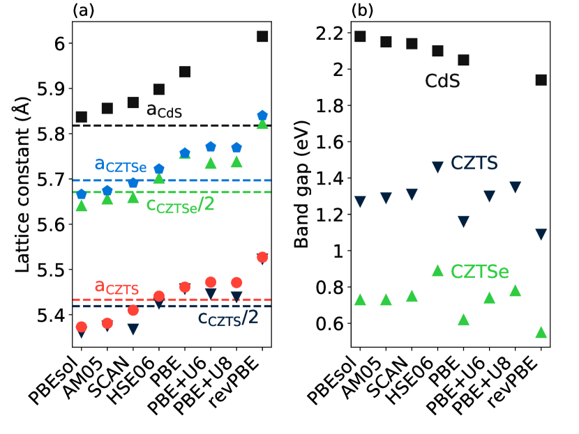
The optimized lattice constants are summarized in Figure 1a. Since CZTS and CZTSe have tetragonal symmetry, there are two lattice constants, which are the lattice constant along (100) and (010) directions, , and that along (001) direction, . The experimentally measured lattice constants (dashed horizontal lines in Figure 1a)Többens et al. (2016); Bosson et al. (2016) are similar to the lattice constants optimized by the SCAN and the HSE06 functionals. The SCAN functional seems better than the PBE functional for the investigation of the CZTS(Se)/CdS interfaces as the PBE overestimates the lattice constant of zb-CdS more than the SCAN does. We also note that is calculated to be generally lower than , consistent with the experiment results.Többens et al. (2016); Bosson et al. (2016) It is also noteworthy that the exchange-correlation functionals are arranged equally in all materials when the optimized lattice constants are sorted with increasing order.
Heavy computational cost of the hybrid calculation can be relieved if the internal coordinates are optimized at the GGA level only.Park and Chan (2018) To find which functional is the most suitable method for this strategy, we obtained the band gap of CdS, CZTS, and CZTSe using the HSE06 functional keeping the structures optimized by various exchange-correlation functionals, as summarized in Figure 1b. The SCAN seems superior to other functionals as it reproduces the closer band gap to the HSE06 value. The band gap can be improved by applying moderate on-site Coulomb potentials, however, larger deviations in the lattice constants were obtained. The result indicates that we can describe the electronic structure cost-effectively by relaxation of the atomic structure using SCAN functional and a subsequent SCF calculation using the HSE06 to correct the band gap of CZTS(Se).
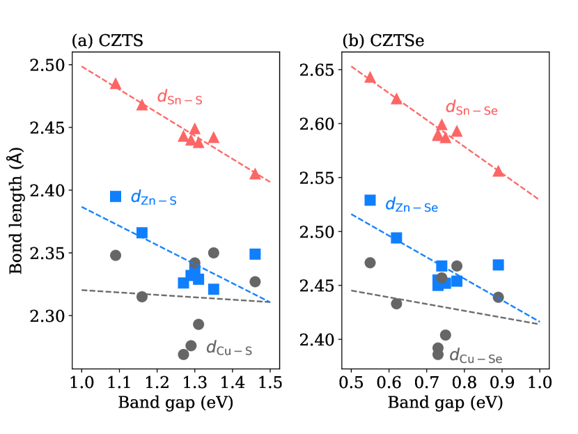
There is no such clear correlation between the lattice constants and the HSE06 band gap of CZTS(Se) summarized in Figure 1b. But the change of the band gap is well explained by the change of the Sn-S(Se) bond length (Figure 2), indicating that the internal coordinates play a significant role in determining the band gap. The conduction band minimum (CBM) of CZTS(Se) is an anti-bonding state of Sn s and S(Se) p orbitals, thus the shortened Sn-S(Se) bond length results in the larger band gap.Park et al. (2015) The average Zn-S(Se) bond length also follows the same trend with larger deviations, whereas the Zn atoms do not constitute the band edges. The low band gap calculated by using the PBE optimized structure is explained by the lengthened Sn-S(Se) bond by 0.05 Å (0.07 Å). Therefore, if the experiment band gap is reproduced by applying large on-site Coulomb potential on Cu d orbitals, then the valence band maximum, which is an anti-bonding state of Cu d and S(Se) p orbitals, could be too deep with respect to the vacuum level within PBE+U calculations. The band gap of zb-CdS increases monotonically with decreasing of the lattice constant because the Cd-S bond length also changes accordingly.
The atomic structure of a (100) CZTS/(100) zb-CdS interface model is shown in Figure 3a. The (100) Miller index of CdS is justified by experimental evidence of the epitaxial growth of CdS on CZTS.Tajima et al. (2014); Liu et al. (2016) The supercell of the interface model includes six CZTS double layers and the same number of zb-CdS double layers. The two lattice vectors parallel to the interface plane were set to [0,,0] and [0,0,], where the lattice constants and are those obtained using the HSE06. A perfectly clean CZTS/CdS interface is expected to have states composed of Cu-S, Zn-S, Sn-S, and/or Cd-S states, in principle. Therefore, the position of the interface states should be affected by the distance between the CZTS layer and the adjacent CdS. To avoid artificially close or distant layers, the cell size along the direction normal to the interface was optimized within 0.01 Å. In each calculation, the CZTS layers were fixed because otherwise it results in the lower HSE06 band gap. The other layers (CdS layers and S atoms at the interfaces) were relaxed using the PBEsol functional until the residual force becomes smaller than 0.03 eV Å-1 because the functional reproduces the atomic structure of zb-CdS most (see Figure 1a). A (100) CZTSe/(100) zb-CdS interface model was generated similarly.
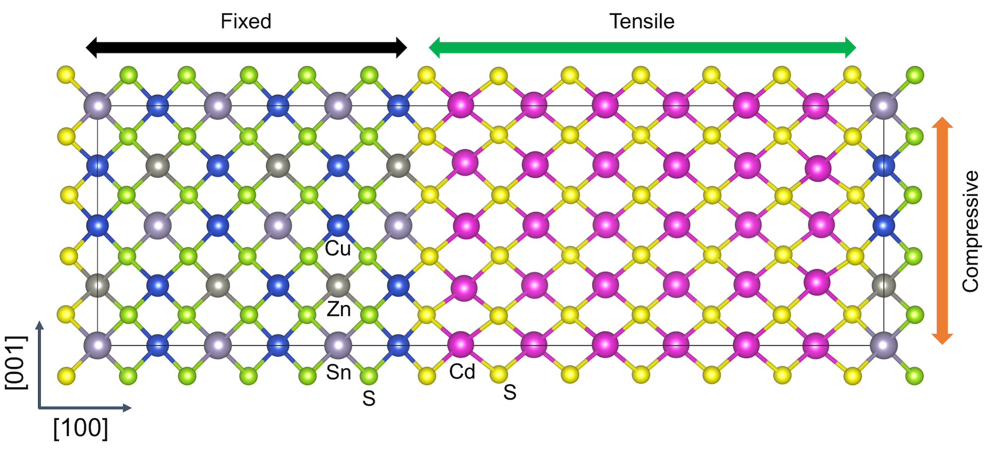
Since CdS has the larger lattice constant than CZTS, a biaxial compressive strain is applied to the CdS layers, and thus the lattice constant along the [100] direction is elongated. When the CdS atoms are optimized with the PBEsol functional, the lattice constant along the [100] direction is increased by 8.3 % in the CZTS/CdS interface model compared to the HSE06 optimized lattice constant (5.90 Å). Much smaller change (1.7 %) is observed in the CZTSe/CdS interface model because of the smaller difference in the lattice constant. This large lattice mismatch between CZTS and CdS will make epitaxial growth difficult in large areas. The epitaxial growth observed in the experiment is probably due to the nanocrystalline nature of CdS.Wuu et al. (1990); Liu et al. (2016)
After we determined the size of the supercell, we optimized the internal coordinates including the CZTS(Se) layers using PBE+U or SCAN+U functionals. Since it is computationally heavy to relax the interface structures using the HSE06 functional, we performed a single SCF calculation with the HSE06 functional using the optimized structures by PBE+U or SCAN+U functionals. The band edges of bulk CZTS(Se) were estimated using the local potential as a reference. The highest occupied states and the lowest unoccupied states in the interface calculations were compared to the estimated band edges.
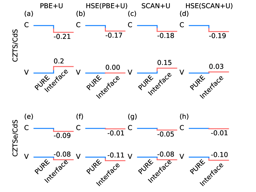
Figure 4 shows the band edge positions calculated from the interface calculation (red) with respect to those obtained from the bulk calculations (blue). Consistent with the previous result, we found the increase of the VBM at the CZTS/CdS interface when PBE+U (Figure 4a) or SCAN+U (Figure 4c) functionals were used.Crovetto et al. (2017) When the electronic structure was calculated using the HSE06 functional, however, there was no evidence of the increased VBM (Figure 4b and Figure 4d). It is also worth emphasizing that the CBM is lowered in every calculation (0.17-0.21 eV) due to the lengthened Sn-S bonds at the interface. Such interface band gap narrowing is not clearly found in CZTSe/CdS interface as the CBM is composed of Sn-Se anti-bonding which is lower than Sn-S anti-bonding.
We also analyzed the electronic structure using the HSE06 functional after we optimized the CdS domain only. In the CZTS/CdS calculation, the CBM of CZTS is lowered by 0.18 eV while the VBM is increased by only 0.01 eV. On the other hand in the CZTSe/CdS calculation, the CBM and the VBM are decreased by 0.03 eV and 0.09 eV, respectively. The CBM of CZTS is reduced no matter whether the CZTS layers were relaxed or not, and thus we rule out an argument that the interface band gap narrowing is caused by the structural relaxation.
We expect that our model is thick enough to confirm nature of the interface band gap narrowing as the electrostatic potential converges quickly as compared to the eigenvalues, which enables a cost-effective estimation of the band edges of pure CZTS(Se).Park et al. (2018b) We also made another CZTS/CdS model by doubling the CZTS and CdS layers, performed a SCAN+U calculation, and found that the reduced CBM of 0.19 eV is reproduced.
We note that the VBM of CZTSe is reduced by 0.1 eV in every calculation as Cu-S bonds are formed at the interfaces in our model. To quantitatively prove this explanation, we substituted Se atoms for S atoms at the interfaces and relaxed the substituted Se atoms using PBE+U functional. The valence band offset (VBO) from the substituted interface was calculated to be -0.03 eV, which is clearly higher in absolute energy than the value before the substitution (-0.08 eV). We note that a slightly higher S composition at the CZTSe/CdS interface could be beneficial as the hole barrier is formed at the interface.
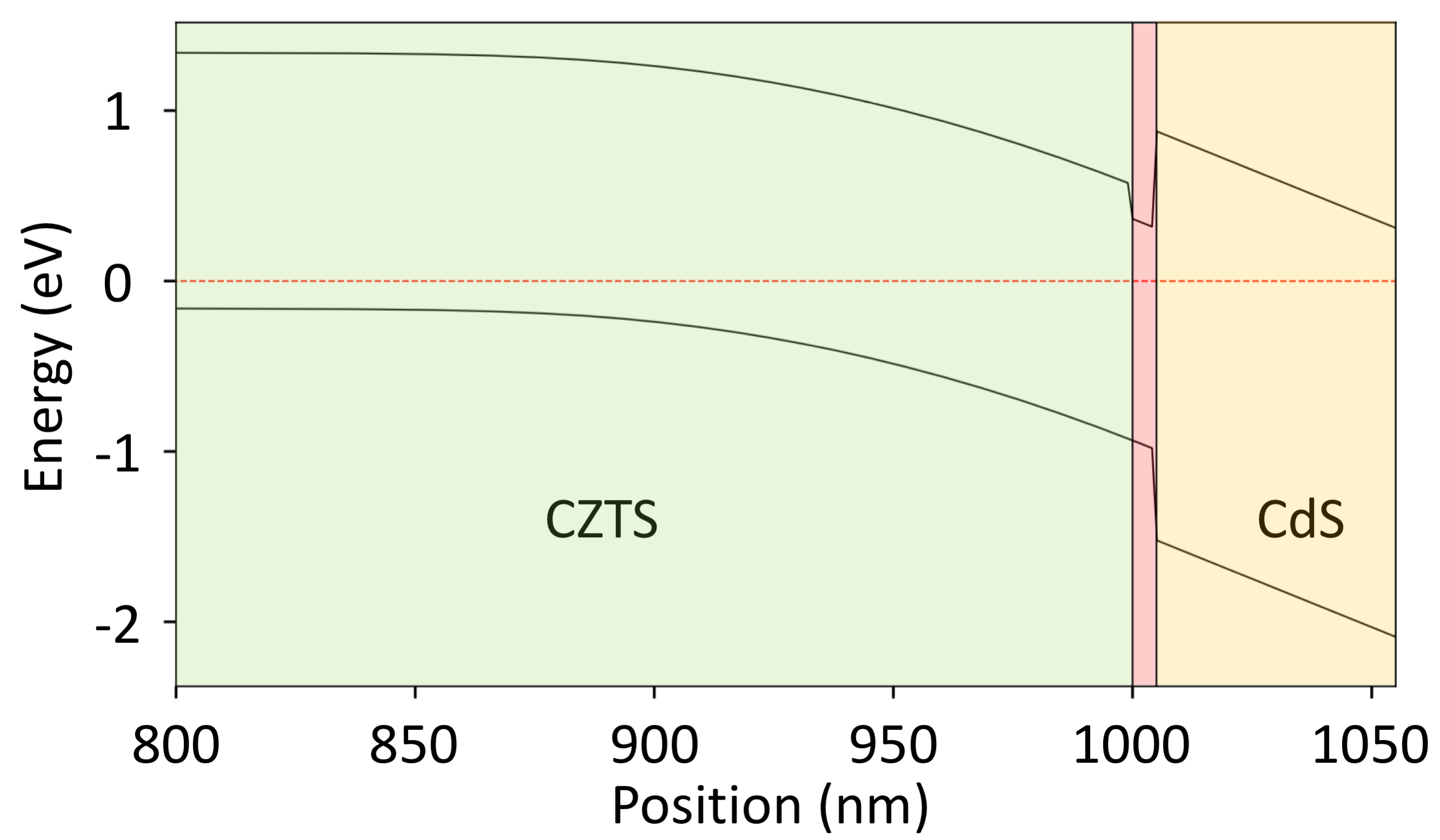
The band diagram of a CZTS/CdS interface was obtained by the solving the Poisson-Boltzmann equation as shown in Figure 5. We adapted the parameters used in another study.Crovetto et al. (2017) Thin layers of CZTS ( 5 nm, red shaded region) is set to have lower conduction band than bulk CZTS by 0.2 eV because of the interface states. The lowered CBM at the interface means that electron charge carriers could be accumulated at the CZTS/CdS interface. The accumulated charges will recombine radiatively or through recombination centers, and then the quasi-Fermi level splitting, which corresponds to the open-circuit voltage, becomes narrower because of the resulting stronger interface recombination.Kim et al. (2018); Neuschitzer et al. (2018)
Based on the calculation results, we suggest that the interface band gap narrowing by the lowered conduction band is an origin of the larger VOC deficit in the CZTS solar cells. Such interface band gap narrowing was not observed in CZTSe/CdS interface, and thus the VOC is less affected by the interface recombination in CZTSe solar cells. Consistent with this expectation, the activation energy for the dominant recombination measured from CZTSe solar cells is almost equivalent to the band gap of the absorber layer.Redinger et al. (2013); Neuschitzer et al. (2015) We also note that the open-circuit voltage deficit has been discussed comprehensively based on the band edge fluctuations.Rau and Werner (2004); Gokmen et al. (2013); Park et al. (2015, 2018c) The band gap fluctuation model, the potential fluctuation model, and the current model based on the interface band gap narrowing do not contradict to each other because the fluctuation happens in bulk regions while the band gap narrowing occurs at the interface.
Experimental studies show that not only the bulk properties but also the interface recombination is essential to improve the CZTS solar cell. The interface can be improved by inserting thin Al2O3 layers between CZTS(Se)/CdS interface,Lee et al. (2016) potentially due to less elemental intermixing.Kim et al. (2017) CZTS solar cells with Zn1-xSnxOy buffer layer also exhibit higher VOC.Ericson et al. (2017) Ge doping was claimed to be effective to reduce the recombination, which mechanism should be investigated further.Neuschitzer et al. (2018) Effect of the light soaking on the cell parameters could be investigated in future studies to widen our understanding.Guo et al. (2010); Neuschitzer et al. (2015); Chantana et al. (2018)
To investigate the electronic structure of CZTS/CdS interface, we employed (100) CZTS/(100) CdS interface. The biaxial tensile strain applied to the CdS layers does not introduce bending in the electrostatic potential, thus we used the potential far from the interface as a reference. When we generated an epitaxial (112) CZTS/(111) CdS interface model, the strong piezoelectric polarization was built along the interface normal direction, resulting in a linear slope in the electrostatic potential.
In summary, we re-examined the electronic structure of the CZTS(Se)/CdS interface and conclude that the bandgap narrowing is caused by a change in the conduction band energy rather than the valence band. We find that a strong on-site Coulomb potential is required to reproduce the HSE06 band gap in GGA+U calculations, while the large on-site Coulomb potential can result in the error in the electron affinity. We also obtained the lattice constants of kesterites and CdS using various exchange-correlation functionals, and suggest a way to reduce errors in the interface calculations.
See supplementary material for the physical properties of CZTS and CZTSe calculated using various exchange-correlation functionals. The primary data for this article is available in a repository at https://zenodo.org/record/1478110.
We thanks Andrea Crovetto and Mattias Lau Nhr Palsgaard for helpful discussion. This project has received funding from the European H2020 Framework Programme for research, technological development and demonstration under grant agreement no. 720907. See http://www.starcell.eu. Via our membership of the UK’s HPC Materials Chemistry Consortium, which is funded by EPSRC (EP/L000202), this work used the ARCHER UK National Supercomputing Service (http://www.archer.ac.uk). We are grateful to the UK Materials and Molecular Modelling Hub for computational resources, which is partially funded by EPSRC (EP/P020194/1). JP thanks the Royal Society for a Shooter International Fellowship.
References
- Polizzotti et al. (2013) A. Polizzotti, I. L. Repins, R. Noufi, S.-H. Wei, and D. B. Mitzi, Energy & Environ. Sci. 6, 3171 (2013).
- Walsh et al. (2012) A. Walsh, S. Chen, S.-H. Wei, and X.-G. Gong, Adv. Energy Mater. 2, 400 (2012).
- Yang et al. (2016) K.-J. Yang, D.-H. Son, S.-J. Sung, J.-H. Sim, Y.-I. Kim, S.-N. Park, D.-H. Jeon, J. Kim, D.-K. Hwang, C.-W. Jeon, D. Nam, H. Cheong, J.-K. Kang, and D.-H. Kim, J. Mater. Chem. A 4, 10151 (2016).
- Guchhait et al. (2016) A. Guchhait, Z. Su, Y. F. Tay, S. Shukla, W. Li, S. W. Leow, J. M. R. Tan, S. Lie, O. Gunawan, and L. H. Wong, ACS Energy Letters 1, 1256 (2016).
- Bourdais et al. (2016) S. Bourdais, C. Choné, B. Delatouche, A. Jacob, G. Larramona, C. Moisan, A. Lafond, F. Donatini, G. Rey, S. Siebentritt, et al., Adv. Energy Mater. 6, 1502276 (2016).
- Grenet et al. (2018) L. Grenet, M. A. A. Suzon, F. Emieux, and F. Roux, ACS Appl. Energy Mater. 1, 2103 (2018).
- Yan et al. (2018) C. Yan, J. Huang, K. Sun, S. Johnston, Y. Zhang, H. Sun, A. Pu, M. He, F. Liu, K. Eder, et al., Nat. Energy 3, 764 (2018).
- Kim et al. (2018) S. Kim, J.-S. Park, and A. Walsh, ACS Energy Letters 3, 496 (2018).
- Gunawan et al. (2010) O. Gunawan, T. K. Todorov, and D. B. Mitzi, Appl. Phys. Lett. 97, 233506 (2010).
- Wang et al. (2014) W. Wang, M. T. Winkler, O. Gunawan, T. Gokmen, T. K. Todorov, Y. Zhu, and D. B. Mitzi, Adv. Energy Mater. 4, 1301465 (2014).
- Crovetto et al. (2017) A. Crovetto, M. L. Palsgaard, T. Gunst, T. Markussen, K. Stokbro, M. Brandbyge, and O. Hansen, Appl. Phys. Lett. 110, 083903 (2017).
- Redinger and Unold (2018) A. Redinger and T. Unold, Sci. Rep. 8, 1874 (2018).
- Repins et al. (2015) I. Repins, J. Li, A. Kanevce, C. Perkins, K. Steirer, J. Pankow, G. Teeter, D. Kuciauskas, C. Beall, C. Dehart, et al., Thin Solid Films 582, 184 (2015).
- Crovetto and Hansen (2017) A. Crovetto and O. Hansen, Sol. Energy Mater. Sol. Cells 169, 177 (2017).
- Kaur et al. (2017) K. Kaur, N. Kumar, and M. Kumar, J. Mater. Chem. A 5, 3069 (2017).
- Antunez et al. (2017) P. D. Antunez, D. M. Bishop, Y. S. Lee, T. Gokmen, O. Gunawan, T. S. Gershon, T. K. Todorov, S. Singh, and R. Haight, Adv. Energy Mater. 7, 1602585 (2017).
- Turnbull et al. (2018) M. J. Turnbull, D. Vaccarello, J. Wong, Y. M. Yiu, T.-K. Sham, and Z. Ding, J. Chem. Phys. 148, 134702 (2018).
- Aberle (2000) A. G. Aberle, Prog. Photovoltaics: Res. Appl. 8, 473 (2000).
- Battaglia et al. (2016) C. Battaglia, A. Cuevas, and S. De Wolf, Energy Environ. Sci. 9, 1552 (2016).
- Park et al. (2018a) J. S. Park, S. Kim, Z. Xie, and A. Walsh, Nat. Rev. Mater. 3, 194 (2018a).
- Wang et al. (2010) K. Wang, O. Gunawan, T. Todorov, B. Shin, S. Chey, N. Bojarczuk, D. Mitzi, and S. Guha, Appl. Phys. Lett. 97, 143508 (2010).
- Redinger et al. (2013) A. Redinger, M. Mousel, M. H. Wolter, N. Valle, and S. Siebentritt, Thin Solid Films 535, 291 (2013).
- Monserrat et al. (2018) B. Monserrat, J.-S. Park, S. Kim, and A. Walsh, Appl. Phys. Lett. 112, 193903 (2018).
- Crovetto et al. (2018) A. Crovetto, A. Cazzaniga, R. B. Ettlinger, J. Schou, and O. Hansen, Sol. Energy Mater. Sol. Cells 187, 233 (2018).
- Heyd et al. (2005) J. Heyd, J. E. Peralta, G. E. Scuseria, and R. L. Martin, J. Chem. Phys. 123, 174101 (2005).
- Wang et al. (2006) L. Wang, T. Maxisch, and G. Ceder, Phys. Rev. B 73, 195107 (2006).
- Jain et al. (2011) A. Jain, G. Hautier, S. P. Ong, C. J. Moore, C. C. Fischer, K. A. Persson, and G. Ceder, Phys. Rev. B 84, 045115 (2011).
- Noh et al. (2011) H.-K. Noh, K. Chang, B. Ryu, and W.-J. Lee, Phys. Rev. B 84, 115205 (2011).
- Blöchl (1994) P. E. Blöchl, Phys. Rev. B 50, 17953 (1994).
- Kresse and Furthmüller (1996) G. Kresse and J. Furthmüller, Phys. Rev. B 54, 11169 (1996).
- Perdew et al. (1996) J. P. Perdew, K. Burke, and M. Ernzerhof, Phys. Rev. Lett. 77, 3865 (1996).
- Zhang and Yang (1998) Y. Zhang and W. Yang, Phys. Rev. Lett. 80, 890 (1998).
- Perdew et al. (2008) J. P. Perdew, A. Ruzsinszky, G. I. Csonka, O. A. Vydrov, G. E. Scuseria, L. A. Constantin, X. Zhou, and K. Burke, Phys. Rev. Lett. 100, 136406 (2008).
- Armiento and Mattsson (2005) R. Armiento and A. E. Mattsson, Phys. Rev. B 72, 085108 (2005).
- Sun et al. (2015) J. Sun, A. Ruzsinszky, and J. P. Perdew, Phys. Rev. Lett. 115, 036402 (2015).
- Heyd et al. (2003) J. Heyd, G. E. Scuseria, and M. Ernzerhof, J. Chem. Phys. 118, 8207 (2003).
- Wei and Zhang (2000) S.-H. Wei and S. B. Zhang, Phys. Rev. B 62, 6944 (2000).
- Többens et al. (2016) D. M. Többens, G. Gurieva, S. Levcenko, T. Unold, and S. Schorr, Phys. Status Solidi B 253, 1890 (2016).
- Bosson et al. (2016) C. Bosson, M. Birch, D. P. Halliday, K. Knight, C. Tang, A. Kleppe, and P. Hatton, in Photovoltaic Specialists Conference (PVSC), 2016 IEEE 43rd (IEEE, 2016) pp. 0405–0410.
- Park and Chan (2018) J.-S. Park and M. K. Chan, J. Appl. Phys. 123, 161560 (2018).
- Park et al. (2015) J.-S. Park, J.-H. Yang, A. Kanevce, S. Choi, I. L. Repins, and S.-H. Wei, Phys. Rev. B 91, 075204 (2015).
- Tajima et al. (2014) S. Tajima, R. Asahi, D. Isheim, D. Seidman, T. Itoh, M. Hasegawa, and K. Ohishi, Appl. Phys. Lett. 105, 093901 (2014).
- Liu et al. (2016) F. Liu, C. Yan, J. Huang, K. Sun, F. Zhou, J. A. Stride, M. A. Green, and X. Hao, Adv. Energy Mater. 6, 1600706 (2016).
- Wuu et al. (1990) D. Wuu, R. Horng, and M. Lee, J. Appl. Phys. 68, 3338 (1990).
- Park et al. (2018b) J.-S. Park, Y.-K. Jung, K. T. Butler, and A. Walsh, arXiv preprint arXiv:1808.00359 (2018b).
- Neuschitzer et al. (2018) M. Neuschitzer, M. Espindola-Rodriguez, M. Guc, J. A. M. Prieto, S. Giraldo, I. Forbes, A. Perez-Rodriguez, and E. Saucedo, J. Mater. Chem. A 6, 11759 (2018).
- Neuschitzer et al. (2015) M. Neuschitzer, Y. Sanchez, S. López-Marino, H. Xie, A. Fairbrother, M. Placidi, S. Haass, V. Izquierdo-Roca, A. Perez-Rodriguez, and E. Saucedo, Prog. Photovoltaics: Res. Appl. 23, 1660 (2015).
- Rau and Werner (2004) U. Rau and J. Werner, Appl. Phys. Lett. 84, 3735 (2004).
- Gokmen et al. (2013) T. Gokmen, O. Gunawan, T. K. Todorov, and D. B. Mitzi, Appl. Phys. Lett. 103, 103506 (2013).
- Park et al. (2018c) J.-S. Park, S. Kim, and A. Walsh, Phys. Rev. Mater. 2, 014602 (2018c).
- Lee et al. (2016) Y. S. Lee, T. Gershon, T. K. Todorov, W. Wang, M. T. Winkler, M. Hopstaken, O. Gunawan, and J. Kim, Adv. Energy Mater. 6, 1600198 (2016).
- Kim et al. (2017) J. Kim, S. Park, S. Ryu, J. Oh, and B. Shin, Prog. Photovoltaics: Res. Appl. 25, 308 (2017).
- Ericson et al. (2017) T. Ericson, F. Larsson, T. Törndahl, C. Frisk, J. Larsen, V. Kosyak, C. Hägglund, S. Li, and C. Platzer-Björkman, Solar RRL 1, 1700001 (2017).
- Guo et al. (2010) Q. Guo, G. M. Ford, W.-C. Yang, B. C. Walker, E. A. Stach, H. W. Hillhouse, and R. Agrawal, J. Am. Chem. Soc. 132, 17384 (2010).
- Chantana et al. (2018) J. Chantana, T. Kato, H. Sugimoto, and T. Minemoto, ACS Appl. Mater. Interfaces 10, 11361 (2018).