Perspective: Dielectric and Ferroic Properties of Metal Halide Perovskites
Abstract
Halide perovskite semiconductors and solar cells respond to electric fields in a way that varies across time and length scales. We discuss the microscopic processes that give rise to the macroscopic polarization of these materials, ranging from the optical and vibrational response to the transport of ions and electrons. The strong frequency dependence of the dielectric permittivity can be understood by separating the static dielectric constant into its constituents, including the orientional polarization due to rotating dipoles, which connects theory with experimental observations. The controversial issue of ferroelectricity is addressed, where we highlight recent progress in materials and domain characterization, but emphasize the challenge associated with isolating spontaneous lattice polarization from other processes such as charged defect formation and transport. We conclude that CH3NH3PbI3 exhibits many features characteristic of a ferroelastic electret, where a spontaneous lattice strain is coupled to long-lived metastable polarization states.
I Introduction
Semiconducting halide perovskite materials have attracted intense research interest over the past five years due to the potential for inexpensive solution processing, and desirable optoelectronic properties for photovoltaic (PV) and light emission applications.Stranks et al. ; Kojima et al. (2009); Gong et al. (2018) Halide perovskites synthesize with the chemical formula \ceABX3, where A is a positively charged cation located in the central cavity created by an extended framework of corner-sharing \ceBX6 metal-halide octahedra.
Thin-film devices based upon the hybrid organic-inorganic perovskite (\ceMAPbI3) were the first to utilize a halide perovskite as the PV absorber layer.Kojima et al. (2009); Lee et al. (2012) This material features prominently in the literature due to the rapid increase in power conversion efficiency (PCE), from 3.8 to 23.3.Shin et al. (2017); Google Scholar However, \ceMAPbI3 has been shown to be chemically unstable and contains the toxic element Pb.Yang and Kelly (2017); Lucia et al. Therefore, materials with elemental compositions including: A = \ceCH3(\ceNH2)2+ (FA), Cs+, Rb+;Koh et al. (2014); Eperon et al. (2015); Protesescu et al. (2015); Saliba et al. (2016a) B = Sn2+, and Ge2+;Noel et al. (2014); Hao et al. (2014); Gu et al. (2000) and X = Br-, and Cl-,Edri et al. (2013); Kulbak et al. (2016); Hui et al. ; Chen et al. (2015) as well as numerous 2-D layered perovskites,Gong et al. (2018); Tsai et al. (2016); Jinwoo et al. have been widely studied. The best performing PV devices (PCE and lifetime) are based upon the mixed-cation, mixed-halide perovskite (Cs,MA,FA)Pb\ce(I,Br)3 and are currently the most promising route to commercialize the technology.Saliba et al. (2016b); NREL ; OPV
MAPbI3 has been shown to form in three perovskite structures: a high-temperature cubic Pmm phase stable above 330K; a tetragonal phase (I4/mm or I4/mcm) between 330K and 160K; and a final low-temperature orthorhombic phase (Pnma) stable below 160K.Baikie et al. (2013) Similar phase behavior is observed for other halide perovskites, with the phase stability and transition temperatures being influenced by factors including the radius ratio of the chemical constituents.Stoumpos et al. (2013); Kieslich et al. (2014); Travis et al. (2016)
A number of models have been proposed to explain the origin of the high performance of halide perovskite solar cells, including: defect tolerance;Joseph et al. Rashba splitting;Amat et al. (2014) large polarons;Frost (2017) and ferroelectric (FE) polarons.Miyata and Zhu (2018) Polar nanodomains, observed by piezoforce microscopy (PFM),Kutes et al. (2014); Coll et al. (2015); Kim et al. (2015); Hermes et al. (2016); Röhm et al. (2017); Strelcov et al. (2017) have also been suggested to contribute towards improved charge separation and transport properties.Frost et al. (2014); Rossi et al. (2018) However, following the confirmation of ionic transport, current-voltage (-) curve hysteresis – typically an indicator of ferroelectricity – has been attributed to the migration of mobile ions rather than spontaneous lattice polarization.Beilsten-Edmands et al. (2015); Meloni et al. (2016) Photo-enhanced ionic conductivity has also been reported.Kim et al. (2018) The most recent effective-circuit models suggest that coupling between electronic and ionic charge at interfaces dominates the charge transport and extraction properties of halide perovskite solar devices, though a consensus is yet to be formed.Moia et al. (2018); Weber et al. (2018)
The dielectric response function describes the long-range response of a material to an external electric field. This can provide information on the underlying physical mechanisms which manifest such diverse behavior. In halide perovskites, differences in the microscopic crystalline properties of samples, experimental or computational methodologies, and nomenclature lead to disparity in dielectric literature which can be confusing to navigate. In this Perspective, we briefly introduce the theory of dielectric polarization in order to critically interpret the polarization mechanisms reported for halide perovskites. Where possible, we highlight publications which employ the ’best practice’ experimental techniques for investigating the dielectric response. Additionally, we contemplate the ferroic nature of halide perovskites that continues to inspire debate in the field.
II Dielectric Polarization in Crystals
A dielectric is defined as a medium which cannot completely screen a static, external, macroscopic electric field from its interior due to physical constraints on charge rearrangement.of Encyclopaedia Britannica (2011) The response of a dielectric to an applied electric field is described by the theory of dielectric polarization and is usually framed within classical electrodynamics.Jackson (2012); Zangwill (2013)
An external electric field will act to distort the ground-state charge density of a dielectric material with which it interacts –– schematically shown in the inset diagrams of Figure 1. If the displacement is such that the centre of positive charge no longer corresponds to the centre of negative charge, a polarization field, P, is induced; that is, the material becomes polarized. The polarization field opposes the direction of the external field, the effect of which is to reduce (screen) the electric field present in the bulk material, E, when compared to the electric field present in the absence of a dielectric (). Considering only the dielectric response of the electronic charge density, and in the small, static, linear limit, a dielectric obeys the constitutive equation:Wooten (1972)
| (1) |
where, is the dielectric permittivity, (sometimes written ), is the vacuum permittivity or, equally, the permittivity of free space, and we have introduced the auxillary vector field, . The dielectric permittivity is a complex function () of the frequency of the applied field () that quantifies the linear dielectric response of a material to a constant applied field.
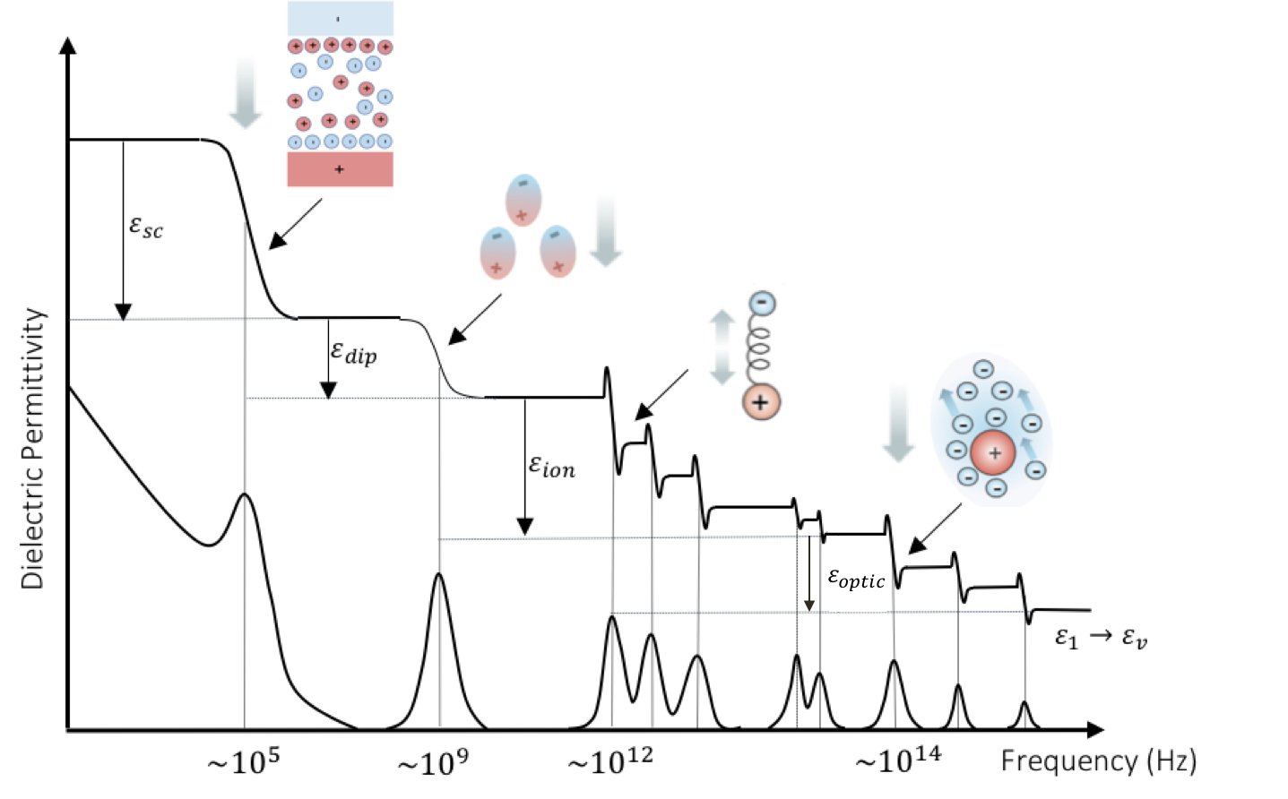
In complex materials, such as the halide perovskites, multiple dielectric mechanisms (physical processes which manifest dielectric polarization) are present.Zheludev (1971) If the same assumptions as above are taken, the contributions from these mechanisms toward the dielectric permittivity are additive, such that we may write:
| (2) |
where is the relative permittivity and we have dropped the frequency dependency for ease of notation. The optical dielectric response, , is due to the (femtosecond) response of the electron density. The ionic contribution, , is due to the (picosecond) response of lattice vibrations (phonon modes), and is proportional to the polarity of the chemical bonds and the softness of the vibrations.Zangwill (2013) The orientational component, , is due to the slower (nanosecond) realignment of any dipolar species.Kirkwood (1939) The space charge contribution, , results from free charges (both ionic and electronic) redistributing (in microseconds to seconds) over macroscopic distances in the material.Kao (2004a) The theoretical and practical considerations necessary to perform computational or experimental investigations of these processes shall be outlined in the following subsections, though we point the reader to Ref. Martin, 2004; Spaldin, 2012 for in-depth reviews on the core topics.
II.1 Dielectric polarization in theory
The dielectric polarization of a solid is often defined as the sum of the induced dipole of a polarizable unit, divided by the volume of the unit.Ashcroft and Mermin (1976) This approach is well defined for finite ionic systems and forms the theoretical foundation of the Clausius-Mossotti model.Felderhof et al. (1983) However, it breaks down in the thermodynamic limit (e.g. for extended crystals with delocalized, periodic electronic wavefunctions), as the charge density cannot be unambiguously decomposed into local contributions.Resta and Vanderbilt (2007); Walsh et al. (2018)
The modern theory of polarization utilizes the framework of density functional theory (DFT) to contemplate the response of the electron wavefunctions in terms of a geometric (Berry) phase, and not as a charge density.Kohn and Sham (1965); Kohn et al. (1996) Consequently, the mathematical formalism which we introduce in the following subsection only addresses the dielectric response of electrons and ions. The theoretical formalism describing the orientational and the space-charge dielectric response shall be presented in Section III.
The quantity of interest in the modern theory is the change in polarization, . It is common in the literature to assume the Born-Oppenheimer approximation in order to separate the change in polarization associated with the response of electrons and ions:Resta (1994)
| (3) |
Using DFT one can represent the electronic charge density in terms of the eigenfunctions of the Kohn-Sham (KS) Hamiltonian (the KS orbitals), . The change in electronic polarization, , that is induced upon an adiabatic transformation () may then be written:Resta (1992)
| (4) |
where the partial derivative, , is taken with respect to – a variable of the KS Hamiltonian which parameterizes the transformation, and which is chosen to take the value of zero and one at the initial and final state, respectively. If is taken to be time, for example, then the change in polarization may be cogitated as the integrated polarization current. The derivative is often stated in terms of first-order density functional perturbation theory (DFPT):King-Smith and Vanderbilt (1993)
| (5) |
where and are the electron mass and bare charge, respectively, is the Kohn-Sham eigenvalue and is the occupation number of state n, is the derivative of the Kohn-Sham potential with respect to , and c.c. refers to charge conjugate terms. The modern theory assumes that the transition from state occurs at null electric field, such that periodic boundary conditions are valid for any value of . In this regime the KS orbitals take the Bloch form, , and Eq. 5 may be recast into a form in which conduction states do not explicitly appear:King-Smith and Vanderbilt (1993); Thouless et al. (1982)
| (6) |
The right hand side of Eq. 6 is closely related to the Berry phase of band n.Ber (1984); Zak (1989) The modern interpretation of electronic polarization in solids therefore states that is proportional to the change in Berry phase. One can further develop this expression by Fourier transforming the Bloch states to define one-electron Wannier centres, the displacement of which is proportional to the electronic polarization.King-Smith and Vanderbilt (1993); Wannier (1960)
One may define the electronic dielectric response as the derivative of the polarization with respect to the macroscopic electric field with the nuclei at fixed positions.Baroni et al. (2001)
| (7) |
Here a and b are lattice directions and is the Kronecker-delta. We have introduced the tensorial form of the dielectric response, , as although in the preceding discussion we contemplated the high-symmetry (isotropic) case, a second-rank tensor is required for a general description of all crystal symmetries.
By removing the restriction of static nuclei, one can calculate the dielectric response including lattice vibrations. To do so, it is necessary to introduce the Born-effective charge (BEC) tensor:Butcher et al. (2013)
| (8) |
which is defined as the linear proportionality coefficient relating the polarization induced in lattice direction, a, to a displacement, r, of the sublattice, s, in the lattice direction, b. The asterisk is introduced to state explicitly that it is an effective charge. When combined with knowledge of the phonon eigenmodes, (which one can calculate with DFT using finite-displacements or within perturbation theory), the ionic (vibrational) contribution to the dielectric response may be calculated, using:Gonze and Lee (1997); Petousis et al. (2016)
| (9) |
Here, the summation is over N phonon modes, and are the eigendisplacements of the interatomic force constant matrix, , (asterisk denotes the complex conjugate). Finally, the change in polarization manifest by lattice displacements can be calculated by:Resta (1994)
| (10) |
which takes a similar form to Eq. 4. The modern theory is commonly used in first-principles calculations of crystalline solids.Baroni and Resta (1986); Baroni et al. (2001); Resta (2018) In general, good agreement is found between the magnitude of spontaneous polarization calculated from Eq. 3 and measurements of conventional ferroelectrics. For example, the calculated value of C/m2 for tetragonal \ceBaTiO3 compares well with a measurement of C/m2.Zhong et al. (1994)
II.2 Dielectric polarization in practice
The dielectric polarization of a crystal cannot be reliably measured as an intrinsic, bulk property. Generally, one experimentally measures the change in polarization between two polarization states from hysteresis loops that are generated upon switching the direction of polarization currents.Fukunaga and Noda (2008) The mathematical formalism introduced above was motivated, in part, by a desire to compare theoretical calculations with such measurements.
The majority of studies investigating polarization phenomena today examine its derivatives, however, such as pyro-/piezo-electric coefficients. In the context of solar cells, measurements of the relative permittivity are frequently reported due to its significance in calculations of physical constants (e.g. absorption coefficient) that impact device performance. The complete device-relevant dielectric response occurs over a large frequency range (Hz–PHz), requiring multiple complementary experimental techniques (on inevitably different devices) to fully characterize.
Ellipsometry is an optical technique employed to investigate the electronic dielectric response of crystalline samples.Leguy et al. (2016a); Peter and Cardona (2010) This technique measures the amplitude and phase of (monochromatic) polarized light after reflection off a dielectric surface from oblique incidence. Electromagnetic radiation which is transmitted or reflected from oblique incidence has two possible polarization vectors: (1) in which the plane of oscillation is the same for incident and reflected radiation, which we label p-polarization; and (2) in which they are not, which we label s-polarization.SPp Upon reflection, the p- and s-polarizations will manifest different changes in amplitude and phase due to the difference in electric dipole radiation. It is therefore the amplitude ratio (), and phase difference () between p- and s-polarizations which ellipsometry can provide access to. These quantities may be used to determine the amplitude reflection coefficients, and , via the relation:Fujiwara (2007)
| (11) |
where is the reflectivity. The complex refractive index, (), can subsequently be calculated using the general Fresnel equations, seen below, and mapped to the real and imaginary components of the optical dielectric response via the Maxwell relation, .Agranovich and Ginzburg (1984); Fox (2001)
| (12) |
here and correspond to the angle of incidence and reflectance, respectively, and and are the refractive index of the incident media and of the dielectric, respectively. In conventional semiconductors and insulators, good agreement is found between calculation and measurement of optical dielectric constants. For example, DFPT calculations of for Si correspond well with a measurement of from ellipsometry.A. and J. ; Jellison and Modine (1983)
The dielectric contribution from the response of ions is frequently investigated using infrared (IR) spectroscopy.Stuart (2005) The proportion of light which is transmitted through a dielectric is measured in order to determine the angular frequency of the materials phonon modes. The theory of lattice dynamics describes how, at finite temperatures, ions vibrate around their equilibrium crystallographic positions.Maradudin et al. (1963) This motion may be enhanced by photoabsorption; a phenomena which is magnified when the frequency of the perturbing field approaches the natural frequency of the vibrational mode. The angular frequency of vibrational modes are thus identified as troughs in transmittance spectra. The oscillation of neighbouring atoms of opposite charge may be in-phase (acoustic phonons) or opposite-in-phase (optical phonons). Therefore, optical phonon modes induce polarization fields which contribute toward the macroscopic dielectric response, whereas acoustic phonon modes do not. If the optical dielectric response is known, the angular frequency of optical phonon modes may be related to the ionic dielectric response via the Lyddane-Sachs-Teller relation:Lyddane et al. (1941)
| (13) |
Here the subscripts LO and TO refer to longitudinal optical (oscillation in the direction of motion) and transverse optical (oscillation perpendicular to the direction of motion) phonon modes, respectively. In order to determine both LO and TO phonon modes, it is necessary to perform measurements at both normal and oblique incidence.Berreman (1963) The harmonic approximation is taken in deriving the LST equation. Consequently, Eq. 13 cannot accurately describe systems with strong anharmonicity, molecular reorientation, or charge transport.Chaves and Porto (1973)
Materials which feature lower-frequency responses are often labelled ‘lossy dielectrics’, as the associated dielectric mechanisms are not harmonic (resonant) processes, but instead totally dispersive. As such, optical measurements are not an appropriate probe of this behavior. A common interpretation of the relative permittivity is as: the ratio of the capacitance of a capacitor whose electrodes are separated by vacuum to a capacitor whose electrodes are separated by a dielectric. Impedance spectroscopy, a technique where the dielectric medium is treated as a capacitor, is therefore often employed.Kremer (2002); Barsoukov and Macdonald (2018) This technique requires many considerations and involves complex analysis; the interface between the dielectric and the electrode contacts being an important factor.Gerhardt (1994); Coster et al. (1996)
By performing the techniques introduced above over a range of frequencies (spectroscopic measurements) one can produce a dielectric spectrum as schematically shown in Fig. 1. Discounting resonance effects, the complex refractive index exhibits normal dispersion (monotonically increases as the applied frequency decreases). Resonant behavior dominates when the frequency of the applied field approaches the natural frequency of the underlying dielectric process.Blythe and Bloor (2008) This gives rise to a characteristic peak in the imaginary component (a Lorentzian), and a step function in the real component, as seen in Figure 1. If the frequency of the applied field is above the response time of the process, it cannot respond fast enough to contribute to the screening. Once a spectrum has been measured, contributions from individual dielectric processes can be assessed within the Debye relaxation model:Debye (1929)
| (14) |
Here is the dielectric relaxation time, and , is the static dielectric response. Extensions of the model have been proposed in order to account for the finite width of the relaxation time distribution, and non-linearity in the high-frequency regime present in devices.Cole and Cole (1941, 1942); Davidson and Cole (1950); Havriliak and Negami (1967) Responses can overlap in frequency (e.g. near optical transitions) or may have such broad frequency response that they exceed the measurement window. This makes unambiguous interpretation difficult. Consequently, few materials have a complete dielectric function characterization; fullerenes are one case where a full spectrum is known.Eklund et al. (1995)
III Dielectric properties of Halide Perovskites
III.1 Optical dielectric response
Optical absorption involves the photoexcitation of electrons from valence to conduction bands; creating either bound electron-hole pairs (excitons) or free carriers. As such, the optical dielectric response is dominated by the optical band gap and other low energy band-edge states. For MAPb\ceI3, it has been deduced that the valence and conduction bands are composed of hybridized I 5p orbitals and Pb 6p orbitals, respectively.Butler et al. (2015) The optical band gap corresponds to the VB1 CB1 transition at the symmetry point, and has been measured at 1.6eV ( THz). Further excitonic absorption has been suggested at 2.48 eV (600 THz) and 3.08 eV (745 THz).Leguy et al. (2016a)
At room temperature, the potential energy surface for the orientation of the \ceCH3NH3+ ion within the lead-iodide octahedra is soft. Consequently, there is computational sensitivity to the choice of electronic structure Hamiltonian, and level of geometry optimization.Zhou et al. (2015); Brivio et al. (2014) However, DFT calculations applying Eq. 7 within the generalized gradient approximation produce an isotropically averaged value of for a crystal with MA aligned in the low energy direction.Brivio et al. (2013) This result was replicated by Ref. Zhou et al., 2015, whom utilized similar methods.
These calculations compare well with the ‘best practice’ experimental value, ; produced from ellipsometry measurements on single crystals.Leguy et al. (2016a) Leguy et al. also measure the optical response of \ceMAPbI3 thin films, and suggest that the reduction in , from , is due to surface effects.Leguy et al. (2016a) A larger response (6.5) is reported by Hirasawa et al., though we suggest this is due to assumptions taken in data processing and not to an increase in the dielectric response.Hirasawa et al. (1994) Further, we posit that Ref. [Glaser et al., 2015] underestimate the electronic response () due to the classical Lorentz dipole fitting model which is employed. To support this statement, when additional Debye components are included in a later study which employed similar methods, a value closer to the consensus is calculated (5.5).Valverde-Chavez et al. (2015)
The polarizability of a compound, and hence the electronic dielectric response, is inversely proportional to the magnitude of its band gap, as described by second-order perturbation theory.Dr L Del Debbio For halide perovskites, a number of general trends related to changes in the band gap can therefore be observed in the published values of summarized in Table LABEL:table:1 for different \ceABX3 compounds.
The decrease in reported values of on transition from I (5p) to Br (4p) to Cl (3p) has been understood by considering the higher binding energy of valence electrons and the corresponding increases in optical band gap ( eV eV eV).Shi et al. (2015); Maculan et al. (2015); Bokdam et al. (2016) Spin-orbit coupling (SOC) plays an important role in determining the conduction band for compounds which include Pb ( = 82) in their composition. Exchanging Pb for Sn ( = 50) leads to a decrease in the optical band gap ( eV eV) and to the expected increase in .Umari et al. (2014); Stoumpos et al. (2013); Whalley et al. (2017a) While the A-site cations do not directly contribute to the band edge states, they do influence the crystal structure and metal-halide bond strength.Amat et al. (2014) The volumetric decrease on exchanging MA for \ceCs leads to an increase in the optical band gap ( eV eV), and to a decrease in , again.Eperon et al. (2015); Stoumpos et al. (2013); Leguy et al. (2016a)
| Material | |||||||
|---|---|---|---|---|---|---|---|
| C | E | C | E | C | E | E | |
| MAPb\ceI3 | 4.5Brivio et al. (2014) 5.1Jiang et al. (2015); Du (2014) 5.3Menéndez-Proupin et al. (2014) 5.8Pérez-Osorio et al. (2015) 6.0Brivio et al. (2013); Zhou et al. (2015); Ma and Wang (2015) 6.8Bokdam et al. (2016) 7.1Umari et al. (2014) | 4.0Löper et al. (2014) 5.0Glaser et al. (2015) 5.5Valverde-Chavez et al. (2015); Leguy et al. (2016a) 6.5Hirasawa et al. (1994) | 16.6Du (2014) 16.7Brivio et al. (2013) 23.2Bokdam et al. (2016) | 16.5Govinda et al. (2017) 17.8Onoda-Yamamuro et al. (1992) 23.3Poglitsch and Weber (1987) 24.5Anusca et al. 28.5Sendner et al. (2016) | 8.9Frost (2017) | 13Lin et al. (2015) 32.1Green et al. (2014) 32Anusca et al. 36.9Green et al. (2014) | 35Lin et al. (2015) Juarez-Perez et al. (2014) |
| MAPb\ceBr3 | 5.2Bokdam et al. (2016) 6.7Zhao et al. (2017) | 4.0Leguy et al. (2016a) 4.7Glaser et al. (2015) 4.8Tanaka et al. (2003) | 18.3Zhao et al. (2017) | 16.0Govinda et al. (2017) 21.5Poglitsch and Weber (1987) 24.7Onoda-Yamamuro et al. (1992) 27.6Sendner et al. (2016) | 38Anusca et al. | ||
| MAPb\ceCl3 | 4.2Bokdam et al. (2016) | 3.1Leguy et al. (2016a) 4.0Glaser et al. (2015) | 11.9Anusca et al. 19.0Onoda-Yamamuro et al. (1992) 20.8Poglitsch and Weber (1987) 25.8Sendner et al. (2016) | 30Anusca et al. | |||
| MASn\ceI3 | 8.2Umari et al. (2014) | ||||||
| CsPb\ceI3 | 5.3Brgoch et al. (2014) | ||||||
| CsPb\ceBr3 | 20.5*Govinda et al. (2017) | ||||||
III.2 Ionic dielectric response
A description of the position of ions within the lattice at finite temperature involves an interplay between thermal motion and interatomic restoring forces (e.g. hydrogen bonding and Van der Waals forces). It is common to assume that the motion is elastic and non-dissipative Рdefined as the harmonic approximation. Anharmonic interactions can also occur, however, and have been suggested in \ceMAPbI3 due to Pb off-centering and octahedral tilting.Whalley et al. (2016); Young et al. (2015) Despite this, the harmonic phonon dispersion has been fully characterized for \ceMAPbI3; and is found to be dominated by vibrations of the \cePbI6 octahedra from THz.P̩rez-Osorio et al. (2015); Leguy et al. (2016b) The low energy of these modes can explain why values for seen in Table LABEL:table:1 for the halide perovskites are much larger than for tetrahedral semiconductors such as \ceCdTe ().Strauch (2012) The strength of the ionic polarization has been suggested to enhance PV performance (e.g. through defect tolerance) and should be an important consideration in future material searches.Wehrenfennig et al. (2013); Brandt et al. (2015); Ganose et al. (2017); Walsh and Zunger (2017)
The averaged BEC tensors for \ceMAPbI3 have been calculated to be larger than the formal ionic charges (, ), such that small ion displacements result in large changes to the polarization.Pérez-Osorio et al. (2015); Du (2014) Anisotropy in the calculated BEC tensors indicates a preferential direction of vibration for apical and equatorial iodine ions, which has been interpreted as octahedral ‘breathing’.Du (2014) Brivio et al. report an isotropically averaged value of for the case when MA is oriented in the low energy direction, which rises to , when MA is oriented in the direction.Brivio et al. (2013). Whilst it is tempting to average over all possible orientations, as done in Ref. Bokdam et al., 2016, we report values associated with MA aligned in the direction, when possible.
These calculations compare well with the ‘best practice’ experimental value of , determined from impedance measurements performed on powder samples.Onoda-Yamamuro et al. (1992) In order to account for the dielectric contribution from interfacial polarization (to be introduced in Section III.D), the authors introduce additional Maxwell-Wagner terms to the Debye relaxation model with which they perform their spectral fitting.Govinda et al. (2017); Sillars (1937) The neglect of these effects can explain the larger value for (23.0) obtained by Poglitsch et al. in an earlier study.Poglitsch and Weber (1987) Sendner et al. report a value of (which rises to 31 if is used) after identifying TO (0.96 THz and 1.9 THz) and LO (1.2 THz and 4.0 THz) phonon modes, and applying the Cochran-Cowley expression.Sendner et al. (2016) The Cochran-Cowley expression is a generalization of Eq. 13 that accounts for systems with more than two atoms in the unit cell (\ceMAPbI3 has 48 at room temperature).Cochran and Cowley (1962) Whilst this value may improve if a greater number of optical phonon modes are included in the calculation (\ceMAPbI3 has 141 at room temperature), it exemplifies the limitations of the model for describing complex materials.
The ionic dielectric response is dependent upon the frequency of vibrational modes and the associated ionic charges. Therefore, compositions containing lighter elements may be expected to exhibit a weaker response due to faster vibrations and less polarizable ions. Contemplating the role of the halide, Ref. [Poglitsch and Weber, 1987] measure a systematic decrease of for the sequence MAPb(I)3 (Br)3 (Cl)3. The authors attribute this behavior to the blue-shift of vibrations associated with the decrease in mass of the halide; an argument supported by Sendner et al.Sendner et al. (2016) Whilst, phonon modes greater than 10 THz associated with \ceCH3NH3 molecular vibration are influential in phase transitions (as seen in Fig. 2), Bokdam et al. suggest that they have little impact on the ionic dielectric response.Bokdam et al. (2016) The measurement of similar responses for both \ceMAPbI3 and \ceCsPbI3 by Ref. [Govinda et al., 2017] supports this claim. Pb2+ is highly polarisable due to its lone pair (6s2) electrons, and is therefore expected to dominate the ionic dielectric response.Ganose et al. (2017) Lone pair activity with dynamic structural distortions has also been confirmed in Sn2+-based halide perovskites.Fabini et al. (2016)
III.3 Orientational dielectric response
Orientational polarization emerges from the stimulated reorientation of localized dipoles in the bulk of a dielectric. The theoretical description was developed within the context of polar liquids and gases, but the same phase physics can be applied to crystalline materials that contain a dipolar species with rotational degrees of freedom.Wilson (1939) The static permittivity for a polar liquid is described by the Kirkwood-Fröhlich equation,Kirkwood (1939); Fröhlich (1968)
| (15) |
where N is the dipole number density, z is the number of nearest-dipolar neighbours, is the angular separation of neighboring dipoles, is the vacuum permittivity, and is the Boltzmann constant. is sometimes defined as an effective temperature (, where is the Curie temperature) to account for dipole-dipole interactions.Govinda et al. (2017); Onoda-Yamamuro et al. (1992); Rupprecht and Bell (1964) Here, for liquids; however, when applied to crystals it also contains the ionic contribution . The electrical dipole moment, , is the Maclaurin series expansion of the applied field with respect to the internal field (though the first order ‘unperturbed’ static value is commonly used in calculations).Hurst et al. (1988) This value can differ from the effective dipole moment that governs dipole-dipole interactions due to screening by the encasing polarizable medium.Wilson (1939)
Unlike the ‘dynamic’ dielectric mechanisms previously introduced, the orientational component is not expected to impact electron transport.Dinpajooh et al. (2017) Whilst the reasoning for this effect is beyond the scope of this perspective, it can be evidenced by the correspondence between reported values of charge mobility measured for organic and inorganic halide perovskites.Herz (2017) Consequently, the majority of studies contemplating the role A-site dynamics on PV functionality do so within the context of ferroelectricity (landscape of polar domains), and not dielectrics. However, the orientational component can influence the slower motion of mobile ions and the screening of point defects.Zwanzig (1963); Chen et al. (2016)
Application of Onsager theory for a polar liquid estimates the response due to the \ceCH3NH3+ dipoles ( D) to be at T = 300K.Frost (2017) This value corresponds well with a multi-approach measurement on thin films, which reports .Du (2014) We required an effective dipole moment of D in order to reproduce a similar value using Equation 15, however. Reported values of D and D, derived by fitting spectral data with Equation 15, are also smaller than theoretical calculations of the static dipole for \ceCH3NH3+.Poglitsch and Weber (1987); Onoda-Yamamuro et al. (1992) This disparity can arise from interactions with the environment or inter-molecular correlation that are not properly described by the polar liquid model. In contrast to the values above, Anusca et al. assign a stronger orientational response () from impedance measurements on single crystals.Anusca et al. (2017) The preceding discussion demonstrates the uncertainty in the field and the need for further investigation and methodological developments.
t!
III.4 Space charge dielectric response
Beyond the bulk polarization processes previously discussed, understanding of the dielectric response due to the distribution and transport of charged species (molecules, ions, electrons, and holes) is essential to describe and characterize the operational behavior of PV devices. As the name suggests, space-charges are formed by spatial inhomogeneity in the charge distribution which create electrostatic potential gradients. The nature of the space charge formed in a device will depend on the processing history and state of a device (e.g. applied voltage).Maier (2004)
Extended defects – including surfaces, interfaces, and grain boundaries – often act as traps for charged species in semiconductors and can support concentrations of charge carriers and defects well above the bulk equilibrium values. The distribution of charge can enhance the strength of dielectric polarization through the formation of electrical double layers (EDLs) – shown in the inset on the far right of Figure 1. The EDLs behave as conventional capacitors to induce static fields which screen the interfacial charge, and can therefore significantly impact impedance measurements.Ishai et al. (2013)
A formal description of space-charge formation requires a solution of the Poisson-Boltzmann equation, given below rearranged in terms of relative permittivity, which is often performed under various approximations (e.g. Helmholtz, Gouy-Chapman, Stern).Butt et al. (2006); Helmholtz (1853); Gouy, M. (1910); Gouy, G. (1917); Chapman (1913); Stern (1924)
| (16) |
Here is the Laplacian of the electrostatic potential, and is the concentration of charge carriers with charge . The space charge is an integral part in drift-diffusion simulations of operating devices. The inherent complexity of real devices – including interfacial inhomogeneity, high defect densities, and phonon scattering – limits the predictive power of Eq. 16.
Evidence for space charge polarization instead arrives from observation of Jonscher’s law () in low-frequency dielectric spectra ( kHz).Jonscher (1981) Jonscher’s law can be understood by relating the imaginary dielectric constant to the components of the refractive index, . The real refractive index, , describes changes in the phase velocity of electromagnetic propagating through a material. The extinction coefficient, , describes radiation attenuation due to its proportionality to the Beer-Lambert absorption coefficient, . Observation of Jonscher’s law in spectroscopic measurements of \ceMAPbI3 therefore suggests that lossy processes, such as ion migration, dominate at low frequency.Du (2014); Anusca et al.
Presenting an equivalent circuit model, Moia et al. suggest that the accumulation of charged ionic species at the perovskite-electrical contact interfaces modulates the energetic barrier to charge injection and recombination.Moia et al. (2018) It is expected that this effect shall be significantly enhanced under illumination due to an increase in the concentration of free carriers and point defects due to photoexcitation.Kim et al. (2018) As previously mentioned, interfacial charge can impact spectroscopic impedance measurements. Consequently, coupling between electronic and ionic transport has been reported to explain the ‘photoinduced giant dielectric constant’ () measured at low frequencies under illumination.Juarez-Perez et al. (2014); Weber et al. (2018)
In addition to macroscopic space charge effects, hopping polarization emerges from the transition of localized charges () between electrostatically inequivalent lattice sites.Ferreira (1981) The hopping polarizability, , can be calculated byKao (2004a)
| (17) |
where is the ensemble average transition probability at thermal equilibrium, is a prefactor containing an attempt frequency, r is the spatial separation, and is the transition activation energy. When treated as a classical process, the associated dielectric contribution can be approximated via the Clausius-Mossotti relation,
| (18) |
where the sum is over M charged species. However, for systems which feature both space-charge and hopping polarization, it is difficult to analytically separate individual contributions. Consequently, there remains uncertainty regarding the spatial distribution of mobile ions in halide perovskites and the pathways which they migrate through (bulk and surface transport or grain boundaries).
Similar hopping processes may also occur for electron transport. Although electrons and holes exist in the form of diffuse large polarons in the bulk materials,Frost (2017) localization and hopping through an inhomogeneous potential energy landscape associated with charged point and extended defects is likely as in the case of H and V-centres.Whalley et al. (2017b) Again, further investigation on this topic is necessary.
IV Ferroic properties of halide perovskites
IV.1 Are halide perovskites ferroelectric?
In analogy to ferromagnets, ferroelectric materials exhibit a spontaneous and reversible polarization below a characteristic Curie temperature. Some of the highest performing ferroelectric materials – as defined by the magnitude of the spontaneous polarization, the Curie temperature, and the coercive electric field – are oxide perovskites.Yang et al. (2010) In systems such as \ceBaTiO3 and \cePbZr_xTi_1-xO3, spontaneous polarization arises from a displacement of the A or B species from their ideal (cubic) lattice sites.Cohen and Krakauer (1992) Credible ferroelectricity has also been reported in certain halide perovskites; below 563K \ceCsGeCl3 adopts a non-centrosymmetric rhombohedral perovskite structure with lattice polarization along the direction, and exhibits a non-linear optical response.QingTian et al. (2000)
Lossy dielectrics with mobile ions can exhibit apparent ferroelectric signatures. This is exemplified by reports of hysteresis cycles produced from electrical measurements on a banana.Scott (2008) We note that stoichiometry gradients (Hebb-Wagner polarization) in mixed ionic-electronic conductors represent a more complicated case.Maier (2004) When combined with the molecular dipole, this makes classification of the polar nature of \ceMAPbI3 difficult. This uncertainty has led to conflicting reports, such that the tetragonal phase of \ceMAPbI3 has been referred to as: ‘superparaelectric, consisting of randomly oriented linear ferroelectric domains’ from Monte Carlo simulations;Frost et al. (2014) ‘a ferroelectric relaxor’ from dielectric dispersion measurements;Guo et al. (2016) ‘ferroelectric’ on the basis of electrical measurements on single crystals;Rakita et al. (2017) and ‘non-ferroelectric’ from analysis of impedance spectroscopy.Beilsten-Edmands et al. (2015) Interpreting such disparate results is complicated by differences in experimental technique and sample quality.
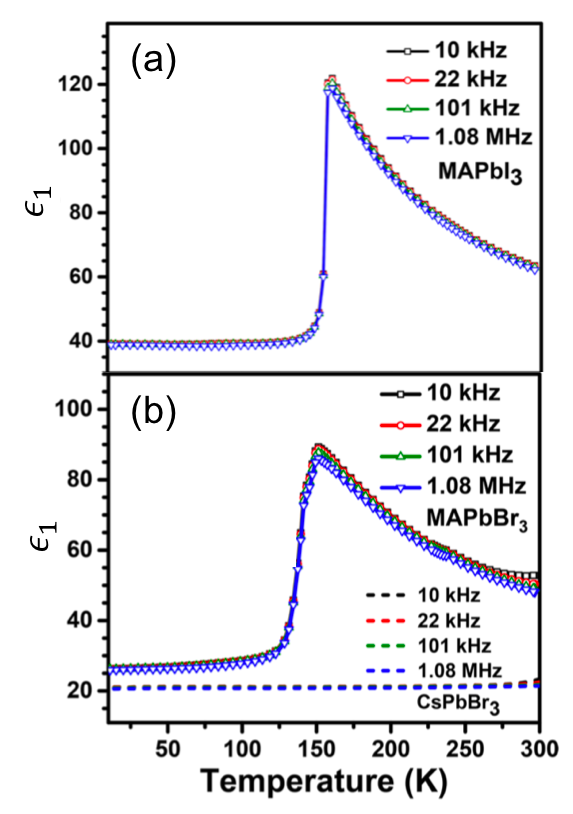
It has been deduced that the \ceCH3NH3+ dipoles have a fixed, anti-aligned orientation in the low-temperature orthorhombic phase of \ceMAPbI3 due to strong hydrogen bonding between the amine group and iodine ions.Svane et al. (2017) The crystal structure is centrosymmetric and anti-polar.Chen et al. (2015) Additional degrees of freedom are introduced upon an increase in the temperature which weaken N\ceH3-I bonds and that enable rotational motion of the organic cation.Weller et al. (2015) Rotational motion induces structural deformations of the inorganic framework due to an asymmetry in the bond strength between iodine and the two functional groups of the \ceCH3NH3+ molecule. Large polarization currents are induced which dramatically impact the dielectric response, as seen in Figure 2(a), and which drive the tetragonal-to-orthorhombic phase transition at low temperature.Birkhold et al. (2018); Gottesman et al. (2014)
In the tetragonal phase, the \ceCH3NH3+ dipole can occupy several fixed orientations within the lattice; the transition between which may be stimulated by thermal motion, for example. Govinda et al. argue that the 1/T dependency of the dielectric response, observed above K in Figure 2(a), implies rotational disorder in the ab plane.Onoda-Yamamuro et al. (1992); Govinda et al. (2017) The established dynamic disorder of molecular orientation and inorganic octahedral titling evidences the absence of true ferroelectricity in \ceMAPbI3.
Following the growing evidence which suggests that polar domains are neither long lived or stable, we suggest that the polar behavior of tetragonal \ceMAPbI3 exhibits many features common to an electret with a combination of lattice, defect, and surface polarization. An electret is defined as a dielectric that contains a mixture of surface or bulk charge, which may be due to real charges or dipoles, and under the effect of an applied voltage decays slowly over time.Kao (2004b) Although one can find reports which claim to contradict this statement, the supporting evidence is consistently inconclusive upon close inspection and comparison between reports.
Beyond hybrid organic-inorganic perovskites that contain polar cations, similar behavior is observed in inorganic halide perovskites (such as CsPb\ceBr3 and CsPb\ceI3) due to fluctuating rather than permanent electric dipoles.Kao (2004a)
IV.2 Are halide perovskites ferroelastic?
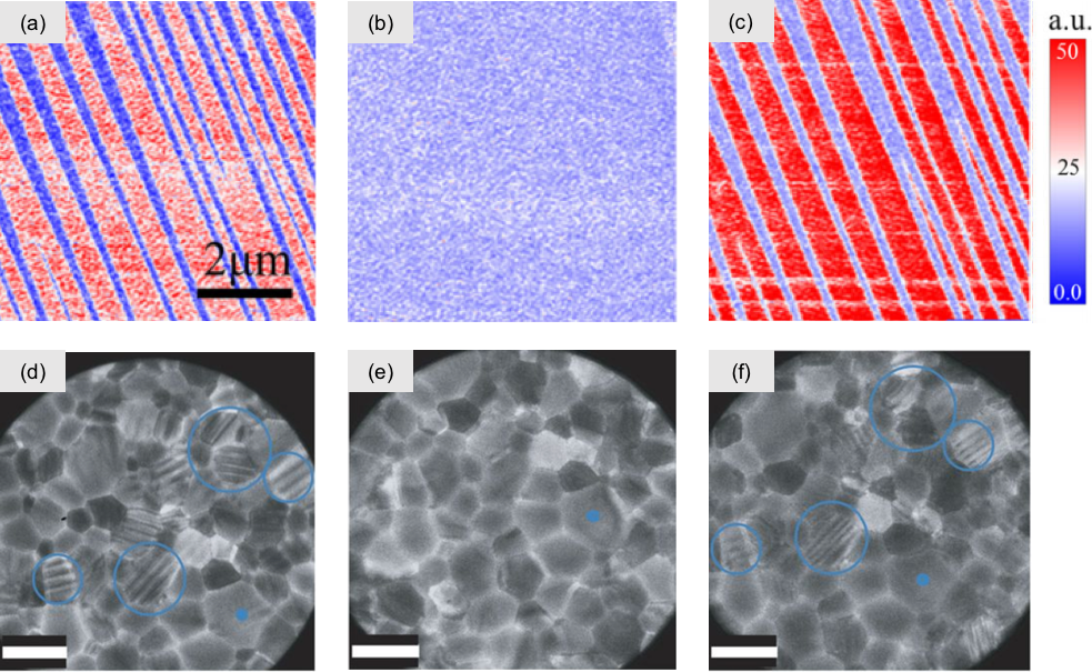
A ferroelastic material exhibits a spontaneous and reversible strain following a stress-induced phase transition. The formation of domains occurs in order to minimize the total strain within the material, as established for \ceBaTiO3.Arlt (1990); Chou et al. (2000) The most convincing evidence for ferroic behavior in \ceMAPbI3 thin films comes from observation of domain structures in piezoforce microscopy (PFM) amplitude and transmission electron microscopy (TEM) images, shown in Figure 3.Huang et al. (2018); Rothmann et al. (2017) These have been classified as ferroelastic twin domains.
‘Ferroelastic fingerprints’ were revealed by early PFM measurements on these materials.Hermes et al. (2016); Strelcov et al. (2017) Methodological refinements improved the precision of the PFM technique, such that a transformation of the domain structures upon heating and cooling through the cubic-to-tetragonal phase transition can be conclusively observed in Ref. Huang et al., 2018; Vorpahl et al., 2018. In analogy to \ceBaTiO3, this suggests that the cubic phase is prototypic, and that the cubic-to-tetragonal phase transition is stress induced.Aizu (1970)
Observation of the same structures and behavior in TEM, shown in Figures 3(d-f), implies that the domain structures extend into the bulk material.Rothmann et al. (2017) Moreover, they confirm that the measured PFM signal is not merely due to polarization fields. Rothmann et al. suggest that such structures ‘eluded observation so far […] due to their very fragile nature under the electron beam’ and therefore utilized a low electron dose rate (Å) during their TEM experiment to mitigate these effects.Rothmann et al. (2017) Further support for the assignment of \ceMAPbI3 as ferroelastic arrives from reports of a lattice constriction,Ren et al. (2016) stress induced modifications to domain wall positions,Strelcov et al. (2017), and periodic differences in the resonant frequency of MA+ dipolar oscillations.Liu et al. (2018a, b); Huang et al. (2018)
It is clear that whilst there is sufficient evidence to support the assignment of the domains forming in \ceMAPbI3 as ferroelastic, that these alone cannot explain the full range of observed behavior. After all, ferroelastic “domains cannot be probed by PFM”, as Röhm et al. points out.Röhm et al. (2017) However, as seen for the case of \ceGaV4S8, polar domains in which ferroelastic strain is the primary order parameter can be observed.Butykai et al. (2017) The ferroic properties of halide perovskites seem characteristic of a ferroelastic electret. A ferroelastic electret can be defined as a dielectric in which the primary order parameter, the spontaneous strain, is coupled to a quasi-permanent polarization.
Similar twin domains have also been observed in the tetragonal phase of , and thin film samples.Gratia et al. (2016); Tan et al. (2017) Notably, the standard annealing procedure at ca. 100∘C means that all \ceMAPbI3 thin-films will be subject to this phase transition. However, it has been reported that alloying \ceMAPbI3 with FA+ based halide perovskites reduces the temperature of the cubic-tetragonal phase transition.Weber et al. (2016) Therefore, we do not expect that these mixed cation compounds will exhibit the same strain-induced deformation at room temperature.
IV.3 Imaging of ferroic domain behavior
The nature of a ferroelastic state may be directly probed by the measurement of elastic hysteresis cycles.Tagantsev et al. (2010); Prasad and Subbarao (1977) Such measurements do not feature in the literature of halide perovskites, however, as the technique is practically challenging. The majority of experimental evidence instead arrives from the PFM data maps previously discussed. PFM is a complex technique itself as measurements are sensitive to the effect of electrostatic, ionic and topological artifacts, which makes unambiguous interpretation difficult.Balke et al. (2015) Consequently, characterization of the ferroelastic state and its coupling to a polar response has been complicated by conflicting results.
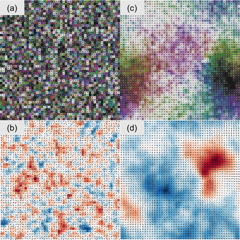
For example, a number of vertical PFM (v-PFM) measurements show lamellar domain contrast between high- and low-response piezoelectric regions – as seen in Figures 3(a & c) – which suggest the existence of multiple response mechanisms.Hermes et al. (2016); Strelcov et al. (2017); Liu et al. (2018c) In support of this, Huang et al. report that electrostatic interactions or ionic activity are responsible for the low piezo-response measured in alternate domains in v-PFM data maps.Huang et al. (2018); Chen et al. (2014); Li et al. (2015) The authors spatially correlate these low response regions with domains in lateral PFM measurements which show no piezo-response and subsequently argue that domain boundaries exist between a polar and a non-polar space group.Huang et al. (2018)
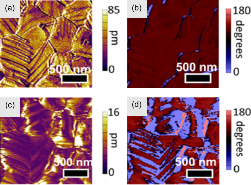
Reports of a consistently non-zero lateral PFM signal and of variation in the piezoresponse being restricted to domain boundaries – as shown in Figure 5 – seem to contradict this behavior.Röhm et al. (2017); Vorpahl et al. (2018); Kutes et al. (2014) Vorpahl et al. suggest instead that inhomogeneity in the PFM amplitude is due to depolarization fields. The authors further argue that their lateral PFM measurement, observed in Figure 5(c), provides evidence that the polarization lies parallel to the surface and that PFM phase contrast, observed in Figure 5(d), emerges due to a offset in the orientation of electrostatic dipoles.Vorpahl et al. (2018)
Polar domain formation is sensitive to the crystal grain size, morphology, and quality.Lines and Glass (1977) Strain can lower the energetic barrier to ionic bond dissociation such that the density of point defects may be significantly enhanced within and between domains.Walsh and Stranks (2018); Jones et al. (2018) This effect can explain twin domain contrast observed in \ceCH3NH3+ chemical composition data maps.Liu et al. (2018b) We suggest that the variation in observed behavior can be linked to differences in initial strain distribution (e.g. due to stoichiometry or substrate effects) and the subsequent response of the crystal.
V Outlook
Hybrid halide perovskites – and organic-inorganic crystals in general – are examples of complex dielectric materials that feature a range of polarization mechanisms. These include the perturbation of the electron clouds around atomic centers, the displacement and rotation of ions and molecules, as well as the transport of charged species (ions and electrons). Based on a survey of the literature for \ceCH3NH3PbI3 we recommend values of for high-frequency processes, for the ionic contribution, which yields a bulk dynamic dielectric response, of .
A rigorous description of even a homogeneous bulk material is challenging and requires a combination of theoretical (statistical mechanical) and experimental techniques. In his 1949 monograph Theory of Dielectrics, Fröhlich noted: “That this application is far from trivial is shown by some of the controversies in the literature”. This is certainly true for the halide perovskites. However, from an assessment of the current literature, we conclude that the intrinsic bulk dielectric response is dominated by the displacement of ions as described the phonon modes of the crystal.
The ferroic properties of \ceMAPbI3 and related materials have attracted significant attention over the past five years. It is difficult to separate lattice polarization from charge transport and surface effects. We highlight the growing evidence supporting the assignment of room-temperature domain structures as ferroelastic, arising from the cubic-to-tetragonal phase transition that occurs during the standard annealing process of thin-films. Such domains can be associated with trapped charged defects and charge carriers. We conclude that halide perovskites can be classified as ferroelastic electrets, which raises many exciting possibilities for engineering their polarization states and lifetimes. A significant amount of work remains in physical characterization of these materials and the development of quantitative models to describe the full range of physical processes at play in operating photovoltaic devices.
Acknowledgements.
We thank P. R. F. Barnes, L. Herz, S. Stranks and R. W. Whatmore for useful discussion on polarization, piezoresponse and perovskites. This research has been funded by the EPSRC (Grant No. EP/K016288/1). AW is supported by a Royal Society University Research Fellowship. We are grateful to the UK Materials and Molecular Modelling Hub for computational resources, which is partially funded by EPSRC (EP/P020194/1).References
- (1) S. D. Stranks, P. K. Nayak, W. Zhang, T. Stergiopoulos, and H. J. Snaith, Angewandte Chemie International Edition 54, 3240.
- Kojima et al. (2009) A. Kojima, K. Teshima, Y. Shirai, and T. Miyasaka, Journal of the American Chemical Society 131, 6050 (2009), pMID: 19366264.
- Gong et al. (2018) X. Gong, O. Voznyy, A. Jain, W. Liu, R. Sabatini, Z. Piontkowski, G. Walters, G. Bappi, S. Nokhrin, O. Bushuyev, et al., Nature materials , 1 (2018).
- Lee et al. (2012) M. M. Lee, J. Teuscher, T. Miyasaka, T. N. Murakami, and H. J. Snaith, Science (2012), 10.1126/science.1228604.
- Shin et al. (2017) S. S. Shin, E. J. Yeom, W. S. Yang, S. Hur, M. G. Kim, J. Im, J. Seo, J. H. Noh, and S. I. Seok, Science 356, 167 (2017).
- (6) . Google Scholar, “”methylammonium lead iodide perovskite” google scholar search,” Accessed: 20-09-2018.
- Yang and Kelly (2017) J. Yang and T. L. Kelly, Inorganic Chemistry 56, 92 (2017), pMID: 27504538.
- (8) S. Lucia, E. Nieves, L. T. Trofod, A. Jose, U. Antonio, and K. F. C., Advanced Energy Materials 5, 1501119.
- Koh et al. (2014) T. M. Koh, K. Fu, Y. Fang, S. Chen, T. C. Sum, N. Mathews, S. G. Mhaisalkar, P. P. Boix, and T. Baikie, The Journal of Physical Chemistry C 118, 16458 (2014).
- Eperon et al. (2015) G. E. Eperon, G. M. Paterno, R. J. Sutton, A. Zampetti, A. A. Haghighirad, F. Cacialli, and H. J. Snaith, Journal of Materials Chemistry A 3, 19688 (2015).
- Protesescu et al. (2015) L. Protesescu, S. Yakunin, M. I. Bodnarchuk, F. Krieg, R. Caputo, C. H. Hendon, R. X. Yang, A. Walsh, and M. V. Kovalenko, Nano Letters 15, 3692 (2015), pMID: 25633588.
- Saliba et al. (2016a) M. Saliba, T. Matsui, K. Domanski, J.-Y. Seo, A. Ummadisingu, S. M. Zakeeruddin, J.-P. Correa-Baena, W. R. Tress, A. Abate, A. Hagfeldt, and M. Grätzel, Science 354, 206 (2016a).
- Noel et al. (2014) N. K. Noel, S. D. Stranks, A. Abate, C. Wehrenfennig, S. Guarnera, A.-A. Haghighirad, A. Sadhanala, G. E. Eperon, S. K. Pathak, M. B. Johnston, et al., Energy & Environmental Science 7, 3061 (2014).
- Hao et al. (2014) F. Hao, C. C. Stoumpos, D. H. Cao, R. P. Chang, and M. G. Kanatzidis, Nature Photonics 8, 489 (2014).
- Gu et al. (2000) Q. Gu, Q. Pan, X. Wu, W. Shi, and C. Fang, Journal of crystal growth 212, 605 (2000).
- Edri et al. (2013) E. Edri, S. Kirmayer, D. Cahen, and G. Hodes, The Journal of Physical Chemistry Letters 4, 897 (2013), pMID: 26291353.
- Kulbak et al. (2016) M. Kulbak, S. Gupta, N. Kedem, I. Levine, T. Bendikov, G. Hodes, and D. Cahen, The Journal of Physical Chemistry Letters 7, 167 (2016), pMID: 26700466.
- (18) Y. Hui, W. Feng, X. Fangyan, L. Wenwu, C. Jian, and Z. Ni, Advanced Functional Materials 24, 7102.
- Chen et al. (2015) Q. Chen, H. Zhou, Y. Fang, A. Z. Stieg, T.-B. Song, H.-H. Wang, X. Xu, Y. Liu, S. Lu, J. You, et al., Nature communications 6, 7269 (2015).
- Tsai et al. (2016) H. Tsai, W. Nie, J.-C. Blancon, C. C. Stoumpos, R. Asadpour, B. Harutyunyan, A. J. Neukirch, R. Verduzco, J. J. Crochet, S. Tretiak, et al., Nature 536, 312 (2016).
- (21) B. Jinwoo, C. Himchan, W. Christoph, J. Mi, S. Aditya, F. R. H., Y. Hoichang, and L. TaeâWoo, Advanced Materials 28, 7515.
- Saliba et al. (2016b) M. Saliba, T. Matsui, J.-Y. Seo, K. Domanski, J.-P. Correa-Baena, M. K. Nazeeruddin, S. M. Zakeeruddin, W. Tress, A. Abate, A. Hagfeldt, et al., Energy & Environmental Science 9, 1989 (2016b).
- (23) NREL, “Best research-cell efficiencies chart,” Accessed: 13-07-2018.
- (24) OPV, “Oxford pv sets world record perovskite solar cell,” .
- Baikie et al. (2013) T. Baikie, Y. Fang, J. M. Kadro, M. Schreyer, F. Wei, S. G. Mhaisalkar, M. Graetzel, and T. J. White, Journal of Materials Chemistry A 1, 5628 (2013).
- Stoumpos et al. (2013) C. C. Stoumpos, C. D. Malliakas, and M. G. Kanatzidis, Inorganic Chemistry 52, 9019 (2013).
- Kieslich et al. (2014) G. Kieslich, S. Sun, and A. K. Cheetham, Chemical Science 5, 4712 (2014).
- Travis et al. (2016) W. Travis, E. N. K. Glover, H. Bronstein, D. O. Scanlon, and R. G. Palgrave, Chem. Sci. 7, 4548 (2016).
- (29) B. Joseph, B. Tonio, E. D. A., H. Gary, K. Leeor, L. YuehâLin, L. Igor, M. S. R., M. Yitzhak, M. J. S., M. D. B., P. Yaron, R. A. M., R. Ilan, R. Boris, S. Oscar, S. Vladan, T. M. F., Z. David, K. Antoine, G. David, and C. David, Advanced Materials 27, 5102.
- Amat et al. (2014) A. Amat, E. Mosconi, E. Ronca, C. Quarti, P. Umari, M. K. Nazeeruddin, M. GrÀtzel, and F. De Angelis, Nano Letters 14, 3608 (2014), pMID: 24797342.
- Frost (2017) J. M. Frost, Phys. Rev. B 96, 195202 (2017).
- Miyata and Zhu (2018) K. Miyata and X.-Y. Zhu, Nature materials 17, 379 (2018).
- Kutes et al. (2014) Y. Kutes, L. Ye, Y. Zhou, S. Pang, B. D. Huey, and N. P. Padture, The Journal of Physical Chemistry Letters 5, 3335 (2014), pMID: 26278441.
- Coll et al. (2015) M. Coll, A. Gomez, E. Mas-Marza, O. Almora, G. Garcia-Belmonte, M. Campoy-Quiles, and J. Bisquert, The Journal of Physical Chemistry Letters 6, 1408 (2015), pMID: 26263143.
- Kim et al. (2015) H.-S. Kim, S. K. Kim, B. J. Kim, K.-S. Shin, M. K. Gupta, H. S. Jung, S.-W. Kim, and N.-G. Park, The Journal of Physical Chemistry Letters 6, 1729 (2015), pMID: 26263341.
- Hermes et al. (2016) I. M. Hermes, S. A. Bretschneider, V. W. Bergmann, D. Li, A. Klasen, J. Mars, W. Tremel, F. Laquai, H.-J. Butt, M. Mezger, R. Berger, B. J. Rodriguez, and S. A. L. Weber, The Journal of Physical Chemistry C 120, 5724 (2016).
- Röhm et al. (2017) H. Röhm, T. Leonhard, M. J. Hoffmann, and A. Colsmann, Energy Environ. Sci. 10, 950 (2017).
- Strelcov et al. (2017) E. Strelcov, Q. Dong, T. Li, J. Chae, Y. Shao, Y. Deng, A. Gruverman, J. Huang, and A. Centrone, Science Advances 3 (2017), 10.1126/sciadv.1602165.
- Frost et al. (2014) J. M. Frost, K. T. Butler, F. Brivio, C. H. Hendon, M. van Schilfgaarde, and A. Walsh, Nano Letters 14, 2584 (2014), pMID: 24684284.
- Rossi et al. (2018) D. Rossi, A. Pecchia, M. A. der Maur, T. Leonhard, H. Röhm, M. J. Hoffmann, A. Colsmann, and A. D. Carlo, Nano Energy 48, 20 (2018).
- Beilsten-Edmands et al. (2015) J. Beilsten-Edmands, G. E. Eperon, R. D. Johnson, H. J. Snaith, and P. G. Radaelli, Applied Physics Letters 106, 173502 (2015).
- Meloni et al. (2016) S. Meloni, T. Moehl, W. Tress, M. Franckevičius, M. Saliba, Y. H. Lee, P. Gao, M. K. Nazeeruddin, S. M. Zakeeruddin, U. Rothlisberger, et al., Nature communications 7, 10334 (2016).
- Kim et al. (2018) G. Y. Kim, A. Senocrate, T.-Y. Yang, G. Gregori, M. Grätzel, and J. Maier, Nature materials 17, 445 (2018).
- Moia et al. (2018) D. Moia, I. Gelmetti, P. Calado, W. Fisher, M. Stringer, O. Game, Y. Hu, P. Docampo, D. Lidzey, E. Palomares, J. Nelson, and P. R. F. Barnes, (2018).
- Weber et al. (2018) S. A. L. Weber, I. M. Hermes, S.-H. Turren-Cruz, C. Gort, V. W. Bergmann, L. Gilson, A. Hagfeldt, M. Graetzel, W. Tress, and R. Berger, Energy Environ. Sci. , (2018).
- of Encyclopaedia Britannica (2011) T. E. of Encyclopaedia Britannica, “Dielectric,” (2011), accessed: October 26, 2018.
- Jackson (2012) J. Jackson, Classical Electrodynamics (Wiley, 2012).
- Zangwill (2013) A. Zangwill, Modern electrodynamics (Cambridge University Press, 2013) Chap. 6.
- Wooten (1972) F. Wooten, in Optical Properties of Solids, edited by F. Wooten (Academic Press, 1972) pp. 15 – 41.
- Zheludev (1971) I. S. Zheludev, “Electric polarization,” in Physics of Crystalline Dielectrics: Volume 2 Electrical Properties (Springer US, Boston, MA, 1971) pp. 337–453.
- Kirkwood (1939) J. G. Kirkwood, The Journal of Chemical Physics 7, 911 (1939).
- Kao (2004a) K. C. Kao, Dielectric phenomena in solids (Academic press, 2004) Chap. 2.
- Martin (2004) R. M. Martin, Electronic structure: basic theory and practical methods (Cambridge university press, 2004) Chap. 22.
- Spaldin (2012) N. A. Spaldin, Journal of Solid State Chemistry 195, 2 (2012).
- Ashcroft and Mermin (1976) N. W. Ashcroft and Mermin, Solid state physics (AAPT, 1976) Chap. 27.
- Felderhof et al. (1983) B. U. Felderhof, G. W. Ford, and E. G. D. Cohen, Journal of Statistical Physics 33, 241 (1983).
- Resta and Vanderbilt (2007) R. Resta and D. Vanderbilt, Physics of Ferroelectrics: A Modern Perspective (Springer Berlin Heidelberg, Berlin, Heidelberg, 2007) pp. 31–68.
- Walsh et al. (2018) A. Walsh, A. A. Sokol, J. Buckeridge, D. O. Scanlon, and C. R. A. Catlow, Nature Mat. 17, 958 (2018).
- Kohn and Sham (1965) W. Kohn and L. J. Sham, Phys. Rev. 140, A1133 (1965).
- Kohn et al. (1996) W. Kohn, A. D. Becke, and R. G. Parr, The Journal of Physical Chemistry 100, 12974 (1996).
- Resta (1994) R. Resta, Rev. Mod. Phys. 66, 899 (1994).
- Resta (1992) R. Resta, Ferroelectrics 136, 51 (1992).
- King-Smith and Vanderbilt (1993) R. D. King-Smith and D. Vanderbilt, Phys. Rev. B 47, 1651 (1993).
- Thouless et al. (1982) D. J. Thouless, M. Kohmoto, M. P. Nightingale, and M. den Nijs, Phys. Rev. Lett. 49, 405 (1982).
- Ber (1984) Proceedings of the Royal Society of London A: Mathematical, Physical and Engineering Sciences 392, 45 (1984).
- Zak (1989) J. Zak, Phys. Rev. Lett. 62, 2747 (1989).
- Wannier (1960) G. H. Wannier, Phys. Rev. 117, 432 (1960).
- Baroni et al. (2001) S. Baroni, S. de Gironcoli, A. Dal Corso, and P. Giannozzi, Rev. Mod. Phys. 73, 515 (2001).
- Butcher et al. (2013) P. N. Butcher, N. H. March, and M. P. Tosi, Crystalline semiconducting materials and devices (Springer Science & Business Media, 2013) Chap. 3 - Phonons.
- Gonze and Lee (1997) X. Gonze and C. Lee, Phys. Rev. B 55, 10355 (1997).
- Petousis et al. (2016) I. Petousis, W. Chen, G. Hautier, T. Graf, T. D. Schladt, K. A. Persson, and F. B. Prinz, Phys. Rev. B 93, 115151 (2016).
- Baroni and Resta (1986) S. Baroni and R. Resta, Phys. Rev. B 33, 7017 (1986).
- Resta (2018) R. Resta, The European Physical Journal B 91, 100 (2018).
- Zhong et al. (1994) W. Zhong, D. Vanderbilt, and K. M. Rabe, Phys. Rev. Lett. 73, 1861 (1994).
- Fukunaga and Noda (2008) M. Fukunaga and Y. Noda, Journal of the Physical Society of Japan 77, 064706 (2008).
- Leguy et al. (2016a) A. M. A. Leguy, P. Azarhoosh, M. I. Alonso, M. Campoy-Quiles, O. J. Weber, J. Yao, D. Bryant, M. T. Weller, J. Nelson, A. Walsh, M. van Schilfgaarde, and P. R. F. Barnes, Nanoscale 8, 6317 (2016a).
- Peter and Cardona (2010) Y. Peter and M. Cardona, Fundamentals of semiconductors: physics and materials properties (Springer Science & Business Media, 2010) Chap. 6.
- (78) “What is the difference between s- and p-polarization states?” Accessed: October 26, 2018.
- Fujiwara (2007) H. Fujiwara, Spectroscopic ellipsometry: principles and applications (John Wiley & Sons, 2007).
- Agranovich and Ginzburg (1984) V. M. Agranovich and V. Ginzburg, Crystal Optics with Spatial Dispersion, and Excitons (Springer, 1984).
- Fox (2001) M. Fox, Optical properties of solids (AAPT, 2001).
- (82) G. M. A. and K. M. J., Progress in Photovoltaics: Research and Applications 3, 189.
- Jellison and Modine (1983) G. E. Jellison and F. A. Modine, Phys. Rev. B 27, 7466 (1983).
- Stuart (2005) B. Stuart, Kirk-Othmer Encyclopedia of Chemical Technology (2005).
- Maradudin et al. (1963) A. A. Maradudin, E. W. Montroll, G. H. Weiss, and I. Ipatova, Theory of lattice dynamics in the harmonic approximation, Vol. 3 (Academic press New York, 1963).
- Lyddane et al. (1941) R. H. Lyddane, R. G. Sachs, and E. Teller, Phys. Rev. 59, 673 (1941).
- Berreman (1963) D. W. Berreman, Phys. Rev. 130, 2193 (1963).
- Chaves and Porto (1973) A. Chaves and S. Porto, Solid State Communications 13, 865 (1973).
- Kremer (2002) F. Kremer, Journal of Non-Crystalline Solids 305, 1 (2002).
- Barsoukov and Macdonald (2018) E. Barsoukov and J. R. Macdonald, Impedance spectroscopy: theory, experiment, and applications (John Wiley & Sons, 2018).
- Gerhardt (1994) R. Gerhardt, Journal of Physics and Chemistry of Solids 55, 1491 (1994), special Symposium in Honor of Professor Arthur S. Nowick.
- Coster et al. (1996) H. G. Coster, T. C. Chilcott, and A. C. Coster, Bioelectrochemistry and Bioenergetics 40, 79 (1996).
- Blythe and Bloor (2008) T. Blythe and D. Bloor, Electrical Properties of Polymers (Cambridge University Press, 2008).
- Debye (1929) P. J. W. Debye, Polar molecules (Chemical Catalog Company, Incorporated, 1929).
- Cole and Cole (1941) K. S. Cole and R. H. Cole, The Journal of Chemical Physics 9, 341 (1941).
- Cole and Cole (1942) K. S. Cole and R. H. Cole, The Journal of Chemical Physics 10, 98 (1942).
- Davidson and Cole (1950) D. Davidson and R. H. Cole, The Journal of Chemical Physics 18, 1417 (1950).
- Havriliak and Negami (1967) S. Havriliak and S. Negami, Polymer 8, 161 (1967).
- Eklund et al. (1995) P. Eklund, A. Rao, Y. Wang, P. Zhou, K.-A. Wang, J. Holden, M. Dresselhaus, and G. Dresselhaus, Thin Solid Films 257, 211 (1995).
- Butler et al. (2015) K. T. Butler, J. M. Frost, and A. Walsh, Mater. Horiz. 2, 228 (2015).
- Zhou et al. (2015) Y. Zhou, F. Huang, Y.-B. Cheng, and A. Gray-Weale, Phys. Chem. Chem. Phys. 17, 22604 (2015).
- Brivio et al. (2014) F. Brivio, K. T. Butler, A. Walsh, and M. van Schilfgaarde, Phys. Rev. B 89, 155204 (2014).
- Brivio et al. (2013) F. Brivio, A. B. Walker, and A. Walsh, APL Materials 1, 042111 (2013).
- Hirasawa et al. (1994) M. Hirasawa, T. Ishihara, T. Goto, K. Uchida, and N. Miura, Physica B 201, 427 (1994).
- Glaser et al. (2015) T. Glaser, C. MÃŒller, M. Sendner, C. Krekeler, O. E. Semonin, T. D. Hull, O. Yaffe, J. S. Owen, W. Kowalsky, A. Pucci, and R. LovrinÄiÄ, The Journal of Physical Chemistry Letters 6, 2913 (2015), pMID: 26267180.
- Valverde-Chavez et al. (2015) D. A. Valverde-Chavez, C. S. Ponseca, C. C. Stoumpos, A. Yartsev, M. G. Kanatzidis, V. Sundstrom, and D. G. Cooke, Energy Environ. Sci. 8, 3700 (2015).
- (107) U. o. E. Dr L Del Debbio, Professor of Theoretical High-Energy Physics, “Quantum mechanics: Lecture 17 - perturbation theory,” Accessed: 13-06-2018.
- Shi et al. (2015) D. Shi, V. Adinolfi, R. Comin, M. Yuan, E. Alarousu, A. Buin, Y. Chen, S. Hoogland, A. Rothenberger, K. Katsiev, Y. Losovyj, X. Zhang, P. A. Dowben, O. F. Mohammed, E. H. Sargent, and O. M. Bakr, Science 347 (2015), 10.1126/science.aaa2725.
- Maculan et al. (2015) G. Maculan, A. D. Sheikh, A. L. Abdelhady, M. I. Saidaminov, M. A. Haque, B. Murali, E. Alarousu, O. F. Mohammed, T. Wu, and O. M. Bakr, The Journal of Physical Chemistry Letters 6, 3781 (2015), pMID: 26722870.
- Bokdam et al. (2016) M. Bokdam, T. Sander, A. Stroppa, S. Picozzi, D. Sarma, C. Franchini, and G. Kresse, Scientific reports 6, 28618 (2016).
- Umari et al. (2014) P. Umari, E. Mosconi, and F. De Angelis, Scientific reports 4, 4467 (2014).
- Whalley et al. (2017a) L. D. Whalley, J. M. Frost, Y.-K. Jung, and A. Walsh, The Journal of Chemical Physics 146, 220901 (2017a).
- Jiang et al. (2015) Y. Jiang, M. A. Green, R. Sheng, and A. Ho-Baillie, Solar Energy Materials and Solar Cells 137, 253 (2015).
- Du (2014) M. H. Du, J. Mater. Chem. A 2, 9091 (2014).
- Menéndez-Proupin et al. (2014) E. Menéndez-Proupin, P. Palacios, P. Wahnón, and J. C. Conesa, Phys. Rev. B 90, 045207 (2014).
- Pérez-Osorio et al. (2015) M. A. Pérez-Osorio, R. L. Milot, M. R. Filip, J. B. Patel, L. M. Herz, M. B. Johnston, and F. Giustino, The Journal of Physical Chemistry C 119, 25703 (2015).
- Ma and Wang (2015) J. Ma and L.-W. Wang, Nano Letters 15, 248 (2015), pMID: 25493911.
- Löper et al. (2014) P. Löper, M. Stuckelberger, B. Niesen, J. Werner, M. Filipic, S.-J. Moon, J.-H. Yum, M. Topič, S. De Wolf, and C. Ballif, J. Phys. Chem. Lett. 6, 66 (2014).
- Govinda et al. (2017) S. Govinda, B. P. Kore, M. Bokdam, P. Mahale, A. Kumar, S. Pal, B. Bhattacharyya, J. Lahnsteiner, G. Kresse, C. Franchini, A. Pandey, and D. D. Sarma, The Journal of Physical Chemistry Letters 8, 4113 (2017), pMID: 28812901.
- Onoda-Yamamuro et al. (1992) N. Onoda-Yamamuro, T. Matsuo, and H. Suga, Journal of Physics and Chemistry of Solids 53, 935 (1992).
- Poglitsch and Weber (1987) A. Poglitsch and D. Weber, The Journal of Chemical Physics 87, 6373 (1987).
- (122) I. Anusca, S. BalÄiÅ«nas, P. Gemeiner, . a. Svirskas, M. Sanlialp, G. Lackner, C. Fettkenhauer, J. Belovickis, V. Samulionis, M. Ivanov, B. Dkhil, J. Banys, V. Shvartsman, Vladimir, and D. C. Lupascu, Advanced Energy Materials 7, 10.1002/aenm.201770107.
- Sendner et al. (2016) M. Sendner, P. K. Nayak, D. A. Egger, S. Beck, C. Muller, B. Epding, W. Kowalsky, L. Kronik, H. J. Snaith, A. Pucci, and R. Lovrincic, Mater. Horiz. 3, 613 (2016).
- Lin et al. (2015) Q. Lin, A. Armin, R. C. R. Nagiri, P. L. Burn, and P. Meredith, Nature Photonics 9, 106 (2015).
- Green et al. (2014) M. A. Green, A. Ho-Baillie, and H. J. Snaith, Nature Photonics 8 (2014).
- Juarez-Perez et al. (2014) E. J. Juarez-Perez, R. S. Sanchez, L. Badia, G. Garcia-Belmonte, Y. S. Kang, I. Mora-Sero, and J. Bisquert, The Journal of Physical Chemistry Letters 5, 2390 (2014), pMID: 26279565.
- Zhao et al. (2017) D. Zhao, J. M. Skelton, H. Hu, C. La-o vorakiat, J.-X. Zhu, R. A. Marcus, M.-E. Michel-Beyerle, Y. M. Lam, A. Walsh, and E. E. M. Chia, Applied Physics Letters 111, 201903 (2017).
- Tanaka et al. (2003) K. Tanaka, T. Takahashi, T. Ban, T. Kondo, K. Uchida, and N. Miura, Solid State Communications 127, 619 (2003).
- Brgoch et al. (2014) J. Brgoch, A. J. Lehner, M. Chabinyc, and R. Seshadri, The Journal of Physical Chemistry C 118, 27721 (2014).
- Whalley et al. (2016) L. D. Whalley, J. M. Skelton, J. M. Frost, and A. Walsh, Phys. Rev. B 94, 220301 (2016).
- Young et al. (2015) J. Young, A. Stroppa, S. Picozzi, and J. M. Rondinelli, Journal of Physics: Condensed Matter 27, 283202 (2015).
- Leguy et al. (2016b) A. M. Leguy, A. R. Goñi, J. M. Frost, J. Skelton, F. Brivio, X. Rodríguez-Martínez, O. J. Weber, A. Pallipurath, M. I. Alonso, M. Campoy-Quiles, et al., Phys. Chem. Chem. Phys. 18, 27051 (2016b).
- Strauch (2012) D. Strauch, New Data and Updates for several III-V (including mixed crystals) and II-VI Compounds (Springer, 2012) Chap. CdTe: dielectric constant, effective charge, pp. 162–163.
- Wehrenfennig et al. (2013) C. Wehrenfennig, G. E. Eperon, M. B. Johnston, H. J. Snaith, and L. M. Herz, Advanced Materials 26 (2013), 10.1002/adma.201305172.
- Brandt et al. (2015) R. E. Brandt, V. Stevanović, D. S. Ginley, and T. Buonassisi, MRS Communications 5, 265–275 (2015).
- Ganose et al. (2017) A. M. Ganose, C. N. Savory, and D. O. Scanlon, Chem. Commun. 53, 20 (2017).
- Walsh and Zunger (2017) A. Walsh and A. Zunger, Nature Mater. 16, 964 (2017).
- Sillars (1937) R. W. Sillars, Electrical Engineers, Journal of the Institution of 80, 378 (1937).
- Cochran and Cowley (1962) W. Cochran and R. Cowley, Journal of Physics and Chemistry of Solids 23, 447 (1962).
- Fabini et al. (2016) D. H. Fabini, G. Laurita, J. S. Bechtel, C. C. Stoumpos, H. A. Evans, A. G. Kontos, Y. S. Raptis, P. Falaras, A. Van der Ven, M. G. Kanatzidis, et al., J. Am. Chem. Soc. 138, 11820 (2016).
- Wilson (1939) J. N. Wilson, Chemical Reviews 25, 377 (1939).
- Fröhlich (1968) H. Fröhlich, Theory of Dielectrics: Dielectric Constant and Dielectric Loss, Monographs on the physics and chemistry of materials (Oxford University Press, 1968).
- Rupprecht and Bell (1964) G. Rupprecht and R. O. Bell, Phys. Rev. 135, A748 (1964).
- Hurst et al. (1988) G. J. B. Hurst, M. Dupuis, and E. Clementi, The Journal of Chemical Physics 89, 385 (1988).
- Dinpajooh et al. (2017) M. Dinpajooh, M. D. Newton, and D. V. Matyushov, The Journal of Chemical Physics 146, 064504 (2017).
- Herz (2017) L. M. Herz, ACS Energy Letters 2, 1539 (2017).
- Zwanzig (1963) R. Zwanzig, The Journal of Chemical Physics 38, 1603 (1963).
- Chen et al. (2016) Y. Chen, H. Yi, X. Wu, R. Haroldson, Y. Gartstein, Y. Rodionov, K. Tikhonov, A. Zakhidov, X.-Y. Zhu, and V. Podzorov, Nature communications 7, 12253 (2016).
- Anusca et al. (2017) I. Anusca, S. Balčiūnas, P. Gemeiner, Š. Svirskas, M. Sanlialp, G. Lackner, C. Fettkenhauer, J. Belovickis, V. Samulionis, M. Ivanov, et al., Adv. Energy Mater. 7, 1700600 (2017).
- Huang et al. (2018) B. Huang, G. Kong, E. N. Esfahani, S. Chen, Q. Li, J. Yu, N. Xu, Y. Zhang, S. Xie, H. Wen, P. Gao, J. Zhao, and J. Li, npj Quantum Materials 3, 30 (2018).
- (151) C. Commons, “Creative commons attribution 4.0 international public license,” Accessed: November 27, 2018.
- Rothmann et al. (2017) M. U. Rothmann, W. Li, Y. Zhu, U. Bach, L. Spiccia, J. Etheridge, and Y.-B. Cheng, Nature communications 8, 14547 (2017).
- Maier (2004) J. Maier, Physical chemistry of ionic materials: ions and electrons in solids (John Wiley & Sons, 2004).
- Ishai et al. (2013) P. B. Ishai, M. S. Talary, A. Caduff, E. Levy, and Y. Feldman, Measurement Science and Technology 24, 102001 (2013).
- Butt et al. (2006) H.-J. Butt, K. Graf, and M. Kappl, Physics and chemistry of interfaces (John Wiley & Sons, 2006) Chap. 4.
- Helmholtz (1853) H. v. Helmholtz, Annalen der Physik 165, 211 (1853).
- Gouy, M. (1910) Gouy, M., J. Phys. Theor. Appl. 9, 457 (1910).
- Gouy, G. (1917) Gouy, G., Ann. Phys. 9, 129 (1917).
- Chapman (1913) D. L. Chapman, The London, Edinburgh, and Dublin Philosophical Magazine and Journal of Science 25, 475 (1913).
- Stern (1924) O. Stern, Berichte der Bunsengesellschaft für physikalische Chemie 30, 508 (1924).
- Jonscher (1981) A. K. Jonscher, Journal of Materials Science 16, 2037 (1981).
- Ferreira (1981) G. L. Ferreira, Journal of Electrostatics 11, 113 (1981).
- Whalley et al. (2017b) L. D. Whalley, R. Crespo-Otero, and A. Walsh, ACS Energy Lett. 2, 2713 (2017b).
- Yang et al. (2010) S. Yang, J. Seidel, S. Byrnes, P. Shafer, C.-H. Yang, M. Rossell, P. Yu, Y.-H. Chu, J. Scott, J. Ager III, et al., Nature nanotechnology 5, 143 (2010).
- Cohen and Krakauer (1992) R. E. Cohen and H. Krakauer, Ferroelectrics 136, 65 (1992).
- QingTian et al. (2000) G. QingTian, P. QiWei, S. Wei, S. Xun, and F. ChangShui, Progress in Crystal Growth and Characterization of Materials 40, 89 (2000).
- Scott (2008) J. F. Scott, Journal of Physics: Condensed Matter 20, 021001 (2008).
- Guo et al. (2016) H. Guo, P. Liu, S. Zheng, S. Zeng, N. Liu, and S. Hong, Current Applied Physics 16, 1603 (2016).
- Rakita et al. (2017) Y. Rakita, O. Bar-Elli, E. Meirzadeh, H. Kaslasi, Y. Peleg, G. Hodes, I. Lubomirsky, D. Oron, D. Ehre, and D. Cahen, Proceedings of the National Academy of Sciences 114, E5504 (2017).
- Svane et al. (2017) K. L. Svane, A. C. Forse, C. P. Grey, G. Kieslich, A. K. Cheetham, A. Walsh, and K. T. Butler, The Journal of Physical Chemistry Letters 8, 6154 (2017), pMID: 29216715.
- Weller et al. (2015) M. T. Weller, O. J. Weber, P. F. Henry, A. M. Di Pumpo, and T. C. Hansen, Chem. Commun. 51, 4180 (2015).
- Birkhold et al. (2018) S. T. Birkhold, H. Hu, P. T. Höger, K. K. Wong, P. Rieder, A. Baumann, and L. Schmidt-Mende, The Journal of Physical Chemistry C 122, 12140 (2018).
- Gottesman et al. (2014) R. Gottesman, E. Haltzi, L. Gouda, S. Tirosh, Y. Bouhadana, A. Zaban, E. Mosconi, and F. De Angelis, The Journal of Physical Chemistry Letters 5, 2662 (2014), pMID: 26277960.
- Kao (2004b) K. C. Kao, Dielectric phenomena in solids (Academic press, 2004) Chap. 5.
- (175) J. M. Frost, “Starrynight documentation,” Accessed: 13-06-2018.
- Arlt (1990) G. Arlt, Journal of Materials Science 25, 2655 (1990).
- Chou et al. (2000) J.-F. Chou, M.-H. Lin, and H.-Y. Lu, Acta Materialia 48, 3569 (2000).
- Vorpahl et al. (2018) S. M. Vorpahl, R. Giridharagopal, G. E. Eperon, I. M. Hermes, S. A. L. Weber, and D. S. Ginger, ACS Applied Energy Materials 1, 1534 (2018).
- Aizu (1970) K. Aizu, Phys. Rev. B 2, 754 (1970).
- Ren et al. (2016) Y. Ren, I. W. H. Oswald, X. Wang, G. T. McCandless, and J. Y. Chan, Crystal Growth & Design 16, 2945 (2016).
- Liu et al. (2018a) Y. Liu, L. Collins, A. Belianinov, S. M. Neumayer, A. V. Ievlev, M. Ahmadi, K. Xiao, S. T. Retterer, S. Jesse, S. V. Kalinin, B. Hu, and O. S. Ovchinnikova, Applied Physics Letters 113, 072102 (2018a).
- Liu et al. (2018b) Y. Liu, L. Collins, R. Proksch, S. Kim, B. R. Watson, B. Doughty, T. R. Calhoun, M. Ahmadi, A. V. Ievlev, S. Jesse, et al., Nature materials (2018b).
- Butykai et al. (2017) Á. Butykai, S. Bordács, I. Kézsmárki, V. Tsurkan, A. Loidl, J. Döring, E. Neuber, P. Milde, S. C. Kehr, and L. M. Eng, Scientific Reports 7, 44663 (2017).
- Gratia et al. (2016) P. Gratia, G. Grancini, J.-N. Audinot, X. Jeanbourquin, E. Mosconi, I. Zimmermann, D. Dowsett, Y. Lee, M. Grätzel, F. De Angelis, K. Sivula, T. Wirtz, and M. K. Nazeeruddin, Journal of the American Chemical Society 138, 15821 (2016), pMID: 27960332.
- Tan et al. (2017) H. Tan, A. Jain, O. Voznyy, X. Lan, F. P. García de Arquer, J. Z. Fan, R. Quintero-Bermudez, M. Yuan, B. Zhang, Y. Zhao, F. Fan, P. Li, L. N. Quan, Y. Zhao, Z.-H. Lu, Z. Yang, S. Hoogland, and E. H. Sargent, Science (2017), 10.1126/science.aai9081.
- Weber et al. (2016) O. J. Weber, B. Charles, and M. T. Weller, J. Mater. Chem. A 4, 15375 (2016).
- Tagantsev et al. (2010) A. K. Tagantsev, L. E. Cross, and J. Fousek, Domains in ferroic crystals and thin films (Springer, 2010) Chap. 7.
- Prasad and Subbarao (1977) V. C. S. Prasad and E. C. Subbarao, Ferroelectrics 15, 143 (1977), https://doi.org/10.1080/00150197708237807 .
- Balke et al. (2015) N. Balke, P. Maksymovych, S. Jesse, A. Herklotz, A. Tselev, C.-B. Eom, I. I. Kravchenko, P. Yu, and S. V. Kalinin, ACS Nano 9, 6484 (2015), pMID: 26035634.
- Liu et al. (2018c) W. Liu, Y. Liu, J. Wang, C. Wu, C. Liu, L. Xiao, Z. Chen, S. Wang, and Q. Gong, Crystals 8 (2018c), 10.3390/cryst8050216.
- Chen et al. (2014) Q. N. Chen, Y. Ou, F. Ma, and J. Li, Applied Physics Letters 104, 242907 (2014).
- Li et al. (2015) J. Li, J.-F. Li, Q. Yu, Q. N. Chen, and S. Xie, Journal of Materiomics 1 (2015), https://doi.org/10.1016/j.jmat.2015.03.001.
- Lines and Glass (1977) M. E. Lines and A. M. Glass, Principles and applications of ferroelectrics and related materials (Oxford university press, 1977).
- Walsh and Stranks (2018) A. Walsh and S. D. Stranks, ACS Energy Letters 3, 1983 (2018).
- Jones et al. (2018) T. W. Jones, A. Osherov, M. Alsari, M. Sponseller, B. C. Duck, Y.-K. Jung, C. Settens, F. Niroui, R. Brenes, C. V. Stan, Y. Li, M. Abdi-Jalebi, N. Tamura, J. Emyr Macdonald, M. Burghammer, R. H. Friend, V. Bulović, A. Walsh, G. J. Wilson, S. Lilliu, and S. D. Stranks, ArXiv e-prints (2018).