Strong interband interaction in the excitonic insulator phase of Ta2NiSe5
Abstract
Excitonic insulator (EI) was proposed in 60’s as a distinct insulating state originating from pure electronic interaction, but its material realization has been elusive with extremely few material candidates and with only limited evidence such as anomalies in transport properties, band dispersions, or optical transitions. We investigate the real-space electronic states of the low temperature phase in Ta2NiSe5 with an atomic resolution to clearly identify the quasiparticle energy gap together with the strong electron-hole band renormalization using scanning tunneling microscopy (STM) and spectroscopy (STS). These results are in good agreement with the EI transition scenario in Ta2NiSe5. Our spatially-resolved STS data and theoretical calculations reveal further the orbital inversion at band edges, which indicates the exciton condensation close to the Bardeen-Cooper-Schrieffer regime.
Many-body interactions in metallic solids often induce insulating states such as Mott insulators through electron-electron interactions and Peierls insulators through electron-phonon interactions Imada et al. (1998). Excitonic insulator (EI) is another type of interaction-driven insulators formed through a purely electronic mechanism from semimetals or semiconductors with small energy gaps Jérome et al. (1967); Halperin and Rice (1968). A valence electron excited to a conduction band leaves a hole in the valence band, and they can pair into an exciton Ashcroft and Mermin (1976). When the carrier concentration and the dielectric constant are unusually small, the hole potential is poorly screened leading to enhanced exciton binding energy greater than the energy gap of the system. Then, the spontaneous exciton formation occurs and these bosonic quasiparticles condense into the same ground state. This unusual condensate, called the EI, results in flat band edges and an enlarged energy gap Jérome et al. (1967). In a semimetal, the electron-hole interaction is relatively weak and the phase transition follows the same way as the condensation of Cooper pairs in Bardeen-Cooper-Schrieffer (BCS) superconductors, while the attractive interaction is strong in a semiconductor and the transition corresponds to the Bose-Einstein condensation of excitons Bronold and Fehske (2006).
While the EI idea was conceived as early as 1967 and demonstrated in artificial double layer systems with gate voltages or strong magnetic fields at very low temperature Payne (1968); Suprunenko et al. (2012); Du et al. (2017); Zhu et al. (2017), only very few materials were elusively suggested to fall naturally into the EI ground state so far. The first experimental suggestion was TmSe1-xTex Neuenschwander and Wachter (1990); Bucher et al. (1991); Wachter et al. (2004) and later La-doped SmS Wachter et al. (1995), which showed anomalous increases of electric resistivity under high pressure and low temperature. Recently, more detailed discussions were carried out on the temperature-driven transition of -TiSe2 Di Salvo et al. (1976); Yoshida and Motizuki (1980); Th. Pillo et al. (2000); Rossnagel et al. (2002); Kidd et al. (2002); Cerellier et al. (2007); Monney et al. (2009, 2010); van Wezel et al. (2010); Monney et al. (2011); Cazzaniga et al. (2012); Monney et al. (2015); Watanabe et al. (2015); Kogar et al. (2017). This case, however, has been heavily debated since the insulating property itself is not observed and the transition apparently involves a charge ordering with a lattice modulation Di Salvo et al. (1976); Yoshida and Motizuki (1980); Th. Pillo et al. (2000); Rossnagel et al. (2002); Cerellier et al. (2007); Monney et al. (2009, 2010, 2011); Kidd et al. (2002); Kogar et al. (2017). That is, the EI mechanism has to compete with others such as the Jahn-Teller effect or the charge-density-wave (CDW) formation Rossnagel et al. (2002); Kidd et al. (2002). At the center of this debate is the complexity of the band structure, valence-band holes at the center of the Brillouin zone (BZ) and excited electrons in three conduction bands at the BZ boundary Monney et al. (2009), which inevitably involves a non-zero momentum phonon in opening a band gap.
On the other hand, Ta2NiSe5 was very recently proposed as an EI even at room temperature and ambient pressure Wakisaka et al. (2009, 2012); Kaneko et al. (2012, 2013); Seki et al. (2014); Lu et al. (2017); Larkin et al. (2017). In contrast to -TiSe2, Ta2NiSe5 has a direct (zero or negative) band gap above the transition temperature 326 K Kaneko et al. (2012, 2013) without any CDW involved. The insulating state at low temperature is evident in a transport measurement Di Salvo et al. (1986) and an angle-resolved photoemission spectroscopy (ARPES) work Wakisaka et al. (2009, 2012); Seki et al. (2014). Thus, Ta2NiSe5 has obvious merits to clarify the exciton condensation. Ta2NiSe5 is a layered material Sunshine and Ibers (1985); Di Salvo et al. (1986) and each layer, as illustrated in Fig. 1, has two Ta and one Ni chains sandwiched by Se atoms within an orthorhombic unit cell Sunshine and Ibers (1985); Di Salvo et al. (1986). It undergoes a second-order phase transition to a monoclinic structure at 326 K with an anomaly in electric resistivity Di Salvo et al. (1986). ARPES experiments revealed a part of band gap below the Fermi level and its enlargement with the unusual flattening of the valence band edge as the temperature decreases Wakisaka et al. (2009, 2012); Seki et al. (2014). A model calculation interpreted these observations as the indication of the EI state Seki et al. (2014). A recent optical spectroscopy experiment measured the temperature-dependent optical gap of Ta2NiSe5 Lu et al. (2017); Larkin et al. (2017). Nevertheless, the strong interband interaction, which is the key feature of the EI phase, has not been unveiled yet.
In this work, we investigate the real-space electronic states of the EI phase in Ta2NiSe5. Atom-resolved local density of states in a real space was obtained using scanning tunneling microscopy (STM) and spectroscopy (STS), which demonstrates the energy gap with sharp peaks at gap edges, corresponding to the flat renormalized band dispersion. Moreover, the orbital characters of band edges were inverted in the insulating phase, which is the evidence of the strong electron-hole band interaction. The excitonic model calculations revealed that the orbital character inversion also implies the semimetallic band structure in the high temperature phase. This leads us to conclude that the EI formation is close to the Bardeen-Cooper-Schrieffer (BCS) regime rather than the Bose-Einstein condensation within the conventional theory of the EI phase.
Single crystals of Ta2NiSe5 were grown using the chemical vapor transport (CVT) method Kim et al. (2016), which were cleaved in situ for STM/S measurements. STM experiments were conducted using commercial cryogenic STMs (Omicron and Unisoku), for 300 and 78 K, respectively. STM topographies were obtained by a constant current mode and a lock-in amplifier was utilized to measure the differential tunneling conductance . The density functional theory (DFT) calculations were performed by using the full-potential linearized augmented plane-wave (FLAPW) band method, as implemented in the WIEN2K package Blaha et al. (2001) with the generalized gradient approximation (GGA) for the exchange-correlation Perdew et al. (1997). The Brillouin zone integration was done with a 28 28 6 k-mesh and the plane-wave cutoff was = 7. The Falicov-Kimball model was used for the exciton model calculation Falicov and Kimball (1969).
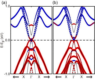
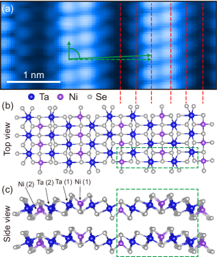
The STM topography taken at 78 K is shown in Fig. 1(a). The topography is largely bias-independent within a relevant energy range of 1 eV, indicating the lack of significant electronic effects such as charge orders or CDW. This is important for the discussion of the transition mechanism. The bias-independence implies that the topography is mainly due to the corrugation of the surface Se layer. Indeed, the topographic contrast matches well with the corrugation of the structure model (Figs. 1(b) and 1(c)) and the x-ray experiment Sunshine and Ibers (1985). The lattice constants measured by STM are a = 3.5 Å and c = 15.4 Å with a monoclinic unit cell in good agreement with the x-ray result for the phase below . Note that this monoclinic structure is a result of the structural transition from an orthorhombic structure at a similar temperature to the electronic transition. Nevertheless, the effect of the structural phase transition on the electronic structure is expected to be negligible compared to the band gap formed through the electronic transition Wakisaka et al. (2009, 2012); Seki et al. (2014); Lu et al. (2017). Our own band structure calculations for orthorhombic and monoclinic structures (Fig. 2) confirm that the band gap opening due to the structural transition is marginal ( 30 meV) sup . Moreover, the entropy change associated with the transition was found to originate mainly from the electronic structure Lu et al. (2017). These results make us focus on the electronic transition.
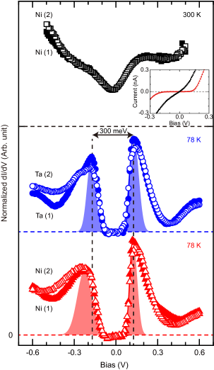
The electronic phase transition is investigated by STS measurements, , which reveals the spatial distribution of local density of states (LDOS) with sub-atomic resolution Feenstra (1994); sup . The room temperature STS data observe finite density of states around the Fermi level although Ta2NiSe5 is reported to have of 325 K (Fig. 3). It obviously reflects the gradual nature of the second-order phase transition with the incomplete gap opening at room temperature together with the thermal broadening of spectral features. In stark contrast, the null density of states near the Fermi level is clear at 78 K (Fig. 3), which evidences an insulating state at low temperature. The metal-insulator phase transition is well supported by the tunneling conductance itself shown in the inset. The energy gap is as large as 300 meV with distinct spectral peaks at gap edges.
The DFT calculations (Fig. 2) cannot explain this huge energy gap even with the structural distortion, and therefore substantial many-body interactions should be introduced for the electronic phase transition. Before we discuss the interband electron-hole interaction, we consider other types of possible many-body interactions. The on-site Coulomb repulsion (or intraband interaction) can be reasonably excluded; it turns out that the energy gap is still closed in a GGA+U calculation with a well-referenced value of 5 eV Schuster et al. (2012) for the on-site Coulomb repulsion of Ni 3 sup . This is because Ta2NiSe5 has large the band width , leading to the small value of , the order parameter of a Mott transition. On the other hand, the possibility of the electron-phonon interaction has to be considered more carefully. Indeed, the electron-phonon interaction is always present and can compete or cooperate with the electron-hole interaction. The previous theoretical study, however, revealed that the electron-phonon interaction cannot open the energy gap solely without the electron-hole interaction but assist the gap opening with a finite electron-hole interaction Kaneko et al. (2013). Within this theory, the contribution of the electron-phonon interaction on the energy gap can be quantitatively estimated. Using the DFT calculation sup , we first estimate the phonon momentum and mode () dependent electron-phonon coupling constants at point 111Phonon modes at point are associated with the structural phase transition between orthorhombic and monoclinic structures.. The largest value of at is 0.1256. In the strong electron-hole interaction regime Kaneko et al. (2013), the energy gap enhancement is only a few tens of meV for the largest electron-phonon coupling constant of 0.1256 222Our value of should be divided by the electronic density of states (1.50 /eV) to be put into this theory.. This gap enhancement is within the energy scale of the relevant phonons Larkin et al. (2018) and the gap size induced by the structural transition discussed above. Thus, one can conclude that the electronic phase transition is driven mainly by the electron-hole interaction while it can be marginally enhanced by the interaction with phonons. We can thus focus on the EI scenario proposed in this material Wakisaka et al. (2009).
The spectral features in Fig. 3 are indeed in good agreement with the EI scenario. Strong peaks at the gap edges would correspond to the flat band edges, which is one of the characteristics of the EI phase Jérome et al. (1967). This is also consistent with the flat valence band maximum observed in ARPES measurements Wakisaka et al. (2009, 2012); Seki et al. (2014). The asymmetry of the peaks reflects the different band dispersion of those flat band edges in the valence and conduction bands (Fig. 5(b)). These spectral features are commonly shown in both calculations for the density of states with the excitonic model and our STS spectrum with Feenstra normalization method sup . Detailed discussion on the different spectral shapes is given below with Fig. 4.
Although the optical gap in the low temperature phase of Ta2NiSe5 was measured in the previous research Lu et al. (2017), the single-particle energy spectrum with the energy gap is identified in the present study. The reported optical gap ( 160 meV) Lu et al. (2017), which was assigned with nearly zero optical conductivity, seems to correspond to the energy window with zero density of states in our STS measurement. Moreover, a broad peak in optical conductivity at 300 - 400 meV seems consistent with the present peak-to-peak energy gap Lu et al. (2017). The valence band maximum relative to the Fermi level was measured as - 175 meV in the previous ARPES study Wakisaka et al. (2012), which agrees excellently with the filled-state resonance peak in the STS measurement. Thus, the energy gap of the low temperature phase is consistently quantified.
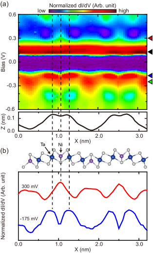
Beyond the energy gap, the spatial distribution of electronic states is investigated in our STS measurements crossing Ta and Ni chains. The differences in point spectra (Fig. 3) are also demonstrated in a spatially resolved LDOS map at 78 K (Fig. 4(a)). Distinct features are observed around 125() and - 175 meV(), which correspond to aforementioned edges of valence and conduction bands, and these states are important for the exciton formation. Both of them carry satellite features at 300() and - 250 meV(), respectively, which have distinct spatial distributions as shown in the figure. While the feature at 125 meV() has little spatial modulation, that at 300 meV() is well localized on Ni sites. On the other hand, the spectral features at - 175() and -250 meV() are localized at Ta and Ni sites, respectively. Note that this localization of each state corresponds to the difference of the spectral intensity in Fig. 3. This spatial LDOS distribution unveils an important aspect of the gap formation. The DFT calculation for Ta2NiSe5 tells us that the bands near the Fermi level are simply composed of parabolic valence and conduction bands from mainly Ni 3 and Ta 5 orbitals, respectively Kaneko et al. (2012, 2013). Our own calculation also confirms this simple band structure (Fig. 2). This contradicts with the STS results where the valence band maximum is localized strongly on Ta and the conduction band minimum has a substantial contribution from Ni atoms. Thus, the strong band renormalization has to be involved in the gap-formation transition between Ta and Ni orbitals or conduction and valence band edges.
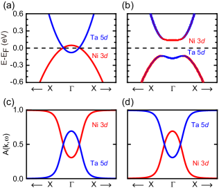
The energy gap formation is further investigated by model calculations Falicov and Kimball (1969); sup . As discussed above, the DFT calculation for the non-interacting band structure with the lattice parameters measured by experiments yields a semimetallic phase with a small negative band gap ( - 50 meV) as shown in Fig. 2(a). In the previous calculation, the conduction (valence) bands were shifted upward (downward) by adding (subtracting) an arbitrary orbital-dependent potential to yield a pre-assumed positive band gap for the high temperature phase Kaneko et al. (2013). However, we cannot find any justification for such an artificial gap opening. As the minimal set of a model Hamiltonian, we extract two bands, each from the valence and the conduction band (Fig. 5(a)). When the coupling of electrons and holes is introduced as a perturbation, the eigenstates near the Fermi level are renormalized with the energy gap opened (Fig. 5(b)). The gap size depends on the coupling strength (), which is related with the exciton binding energy. The renormalized band dispersion at the gap edges is flat together with the substantial hybridization of Ni 3 and Ta 5 orbitals. The STS measurements are largely reproduced by this two-band model calculation with an order parameter meV as shown in Fig. 5(b). That is, the energy gap is opened with a size of 300 meV () and dominant orbital characters at band edges are inverted due to the exciton formation. This inversion is well visualized by the spectral weights of valence (Fig. 5(c)) and conduction bands (Fig. 5(d)) in the EI phase; Ta 5 is stronger than Ni 3 near the point in the valence band and vice versa in the conduction band. Moreover, we can qualitatively estimate the spatial distribution of the electronic states at the valence band maximum from the model calculation. The stronger spectral weight of Ta 5 implies that we have larger density of states on Ta chains than on Ni chains, which is consistent with the normalized profile at the valence band edge (- 175 mV) in Fig. 4(b).
The major limitation of the simple model is that the experiment observes a relatively well-delocalized state at the conduction band minimum together with the Ni-localized state. This might be because Ta2NiSe5 has two degenerate conduction bands and the interaction between these two and the valence band can be more complex than our model. Nevertheless, the present result indicates unambiguously that the observed localization of the valence band edge state at Ta chains cannot be explained without the exciton formation. Moreover, this observation is in contradiction with the semiconductor-to-EI scenario proposed earlier Kaneko et al. (2013). We performed similar model calculations starting from the semiconducting bare band structure and found no inversion of the dominant band characters at edges sup . In other words, the state at the valence band maximum should have been localized at Ni chains if Ta2NiSe5 were a semiconductor in non-interacting phase. That is, the band character inversion is a strong evidence of both the exciton formation and the semimetallic (or zero gap) bare band structure at high temperature. It is largely consistent with an optical spectroscopy data indicating a zero-gap semiconductor at high temperature Lu et al. (2017).
Another limitation is that our simple model Hamiltonian does not take into account the electron-phonon interaction. As discussed above, while its contribution to the energy gap is marginal, the electron-phonon interaction assists the excitonic condensation Kaneko et al. (2013, 2015). In addition, a recent study reported the exciton-phonon coupling mode in the low temperature phase Werdehausen et al. (2018), which makes the further investigation on phonons interesting.
Summarizing all results, Ta2NiSe5 has a metal-insulator transition from a semimetallic non-interacting phase through the strong interband interaction.
No other mechanism than EI can plausibly explain these findings together with the experimental data accumulated up to now, such as the band dispersion renormalization.
Moreover, the present result indicates that the EI phase in this material is close to the BCS mechanism rather than the Bose-Einstein condensation based on the conventional theory Halperin and Rice (1968); Jérome et al. (1967); Bronold and Fehske (2006).
Within this mechanism, the phases of excitons are not coherent above Tc but, as the temperature is lowered, excitons become gradually coherent and spontaneously condense, opening the band gap.
It is notable that the condensation starts from a higher temperature than room temperature in contrast to BCS superconductors.
This is because the binding energy of excitons is two orders of magnitude greater than that of Cooper pairs in BCS superconductors. However, a very recent paper proposed the possibility of a small-gap semiconducting phase above the transition temperature due to preformed excitons in spite of the non-interacting semimetallic bands in Ta2NiSe5 Sugimoto et al. (2018).
Nevertheless, one of our main observations, the orbital character inversion that is the hallmark of a semimetallic non-interacting band, is consistent with this recent paper. The existence of preformed excitons above the transition temperature has to be addressed in future works.
The further control and manipulation of the exciton condensates are highly promising in Ta2NiSe5 with its extremely high transition temperature.
This work was supported by the Institute for Basic Science (Grant No. IBS-R014-D1), the KISTI superconducting center (Grant No. KSC-2014-C3-044), and the Global Ph.D. Fellowship Program of National Research Foundation of Korea.
References
- Imada et al. (1998) M. Imada, A. Fujimori, and Y. Tokura, Rev. Mod. Phys. 70, 1039 (1998).
- Jérome et al. (1967) D. Jérome, T. M. Rice, and W. Kohn, Phys. Rev. 158, 462 (1967).
- Halperin and Rice (1968) B. I. Halperin and T. M. Rice, Rev. Mod. Phys. 40, 755 (1968).
- Ashcroft and Mermin (1976) N. W. Ashcroft and N. D. Mermin, Solid State Physics (Cengage Learing, 1976).
- Bronold and Fehske (2006) F. X. Bronold and H. Fehske, Phys. Rev. B 74, 165107 (2006).
- Payne (1968) R. T. Payne, Phys. Rev. Lett. 21, 284 (1968).
- Suprunenko et al. (2012) Y. F. Suprunenko, V. Cheianov, and V. I. Fal’ko, Phys. Rev. B 86, 155405 (2012).
- Du et al. (2017) L. Du, X. Li, W. Lou, G. Sullivan, K. Chang, J. Kono, and R.-R. Du, Nat. Commun. 8, 1971 (2017).
- Zhu et al. (2017) Z. Zhu, R. D. McDonald, A. Shekhter, B. J. Ramshaw, K. A. Modic, F. F. Balakirev, and N. Harrison, Sci. Rep. 7, 1733 (2017).
- Neuenschwander and Wachter (1990) J. Neuenschwander and P. Wachter, Phys. Rev. B 41, 12693 (1990).
- Bucher et al. (1991) B. Bucher, P. Steiner, and P. Wachter, Phys. Rev. Lett. 67, 2717 (1991).
- Wachter et al. (2004) P. Wachter, B. Bucher, and J. Malar, Phys. Rev. B 69, 094502 (2004).
- Wachter et al. (1995) P. Wachter, A. Jung, and P. Steiner, Phys. Rev. B 51, 5542 (1995).
- Di Salvo et al. (1976) F. J. Di Salvo, D. E. Moncton, and J. V. Waszczak, Phys. Rev. B 14, 4321 (1976).
- Yoshida and Motizuki (1980) Y. Yoshida and K. Motizuki, J. Phys. Soc. Jpn. 49, 898 (1980).
- Th. Pillo et al. (2000) Th. Pillo, J. Hayoz, H. Berger, F. Lévy, L. Schlapbach, and P. Aebi, Phys. Rev. B 61, 16213 (2000).
- Rossnagel et al. (2002) K. Rossnagel, L. Kipp, and M. Skibowski, Phys. Rev. B 65, 235101 (2002).
- Kidd et al. (2002) T. E. Kidd, T. Miller, M. Y. Chou, and T.-C. Chiang, Phys. Rev. Lett. 88, 226402 (2002).
- Cerellier et al. (2007) H. Cerellier, C. Monney, F. Clerc, C. Battaglia, L. Despont, M. G. Garnier, H. Beck, P. Aebi, L. Patthey, H. Berger, and L. Forró, Phys. Rev. Lett. 99, 146403 (2007).
- Monney et al. (2009) C. Monney, H. Cerellier, F. Clerc, C. Battaglia, E. F. Schwier, C. Didiot, M. G. Garnier, H. Beck, P. Aebi, H. Berger, L. Forró, and L. Patthey, Phys. Rev. B 79, 045116 (2009).
- Monney et al. (2010) C. Monney, E. F. Schwier, M. G. Garnier, N. Mariotti, C. Didiot, H. Beck, P. Aebi, H. Cercellier, J. Marcus, C. Battaglia, H. Berger, and A. N. Titov, Phys. Rev. B 81, 155104 (2010).
- van Wezel et al. (2010) J. van Wezel, P. Nahai-Williamson, and S. S. Saxena, Phys. Rev. B 81, 165109 (2010).
- Monney et al. (2011) C. Monney, C. Battaglia, H. Cercellier, P. Aebi, and H. Beck, Phys. Rev. Lett. 106, 106404 (2011).
- Cazzaniga et al. (2012) M. Cazzaniga, H. Cercellier, M. Holzmann, C. Monney, P. Aebi, G. Onida, and V. Olevano, Phys. Rev. B 85, 195111 (2012).
- Monney et al. (2015) G. Monney, C. Monney, B. Hildebrand, P. Aebi, and H. Beck, Phys. Rev. Lett. 114, 086402 (2015).
- Watanabe et al. (2015) H. Watanabe, K. Seki, and S. Yunoki, Phys. Rev. B 91, 205135 (2015).
- Kogar et al. (2017) A. Kogar, M. S. Rak, S. Vig, A. A. Husain, F. Flicker, Y. I. Joe, L. Venema, G. J. MacDougall, T. C. Chiang, E. Fradkin, J. van Wezel, and P. Abbamonte, Science 358, 1314 (2017).
- Wakisaka et al. (2009) Y. Wakisaka, T. Sudayama, K. Takubo, T. Mizokawa, M. Arita, H. Namatame, M. Taniguchi, N. Katayama, M. Nohara, and H. Takagi, Phys. Rev. Lett. 103, 026402 (2009).
- Wakisaka et al. (2012) Y. Wakisaka, T. Sudayama, K. Takubo, T. Mizokawa, N. L. Saini, M. Arita, H. Namatame, M. Taniguchi, N. Katayama, M. Nohara, and H. Takagi, J. Supercond. Nov. Magn. 25, 1231 (2012).
- Kaneko et al. (2012) T. Kaneko, T. Toriyama, T. Konishi, and Y. Ohta, J. Phys.: Conf. Ser. 400, 032035 (2012).
- Kaneko et al. (2013) T. Kaneko, T. Toriyama, T. Konishi, and Y. Ohta, Phys. Rev. B 87, 035121 (2013).
- Seki et al. (2014) K. Seki, Y. Wakisaka, T. Kaneko, T. Toriyama, T. Konishi, T. Sudayama, N. L. Saini, M. Arita, H. Namatame, M. Taniguchi, N. Katayama, M. Nohara, H. Takagi, T. Mizokawa, and Y. Ohta, Phys. Rev. B 90, 155116 (2014).
- Lu et al. (2017) Y. F. Lu, H. Kono, T. I. Larkin, A. W. Rost, T. Takayama, A. V. Boris, B. Keimer, and H. Takagi, Nat. Commun. 8, 14408 (2017).
- Larkin et al. (2017) T. I. Larkin, A. N. Yaresko, D. Pröpper, K. A. Kikoin, Y. F. Lu, T. Takayama, Y.-L. Mathis, A. W. Rost, H. Takagi, B. Keimer, and A. V. Boris, Phys. Rev. B 95, 195144 (2017).
- Di Salvo et al. (1986) F. J. Di Salvo, C. H. Chen, R. M. Fleming, J. V. Waszczak, and R. G. Dunn, J. Less Common Met. 116, 51 (1986).
- Sunshine and Ibers (1985) S. A. Sunshine and J. A. Ibers, Inorg. Chem. 24, 3611 (1985).
- Kim et al. (2016) S. Y. Kim, Y. Kim, C.-J. Kang, E.-S. An, H. K. Kim, M. J. Eom, M. Lee, C. Park, T.-H. Kim, H. C. Choi, B. I. Min, and J. S. Kim, ACS Nano 10, 8888 (2016).
- Blaha et al. (2001) P. Blaha, K. Schwarz, G. Madsen, D. Kvasnicka, and J. Luitz, WIEN2k (Karlheinz Schwarz, Techn. Universität Wien, Austria, 2001).
- Perdew et al. (1997) J. P. Perdew, K. Burke, and M. Ernzerhof, Phys. Rev. Lett. 78, 1396 (1997).
- Falicov and Kimball (1969) L. M. Falicov and J. C. Kimball, Phys. Rev. Lett. 22, 997 (1969).
- (41) See Supplemental Material at [URL will be inserted by publisher] for the detailed calculations.
- Feenstra (1994) R. M. Feenstra, Phys. Rev. B 50, 4563 (1994).
- Schuster et al. (2012) C. Schuster, M. Gatti, and A. Rubio, Eur. Phys. J. B 85, 325 (2012).
- Note (1) Phonon modes at point are associated with the structural phase transition between orthorhombic and monoclinic structures.
- Note (2) Our value of should be divided by the electronic density of states (1.50\tmspace+.1667em/eV) to be put into this theory.
- Larkin et al. (2018) T. I. Larkin, R. D. Dawson, M. Höppner, T. Takayama, M. Isobe, Y.-L. Mathis, H. Takagi, B. Keimer, and A. V. Boris, Phys. Rev. B 98, 125113 (2018).
- Kaneko et al. (2015) T. Kaneko, B. Zenker, H. Fehske, and Y. Ohta, Phys. Rev. B 92, 115106 (2015).
- Werdehausen et al. (2018) D. Werdehausen, T. Takayama, M. Höppner, G. Albrecht, A. W. Rost, Y. Lu, D. Manske, H. Takagi, and S. Kaiser, Sci. Adv. 4, eaap8652 (2018).
- Sugimoto et al. (2018) K. Sugimoto, S. Nishimoto, T. Kaneko, and Y. Ohta, Phys. Rev. Lett. 120, 247602 (2018).