Grain growth in Pt microheaters subjected to high current density under constant power
Abstract
When nm thick Pt microheaters of lateral dimensions m2 are subjected to high electric power their resistance rises, as expected. Following an initial rise however there is a gradual decrement in while constant electric power dissipation is maintained. We find that this lowering in is accompanied by grain growth in the polycrystalline thin Pt film of our heaters. This is confirmed by XRD measurements and SEM imaging. Similar growth in grain size is observed in thin Pt films that are oven-annealed at high temperatures. Thus we argue that maintaining high power dissipation in a microheater has the same effect on its material structure as post-annealing. We observe the in-plane grain size of a 50 nm thick as-grown Pt film/heater to be nm. When post-annealed at a temperature of C for 30 min, nm, compared with when electric current is run through a heater we estimate the mean crystalline length to be nm.
pacs:
Valid PACS appear hereI Introduction
Nano- and micropatterned metal wire structures have attracted significant attention due to their possible applications, which, despite their simplicity might be as varied as serving as microscopic light sourcesHamann, Lacey, and Ingvarsson (2008); Ottonello Briano et al. (2014, 2016), being used in near-field microscopy Cvitkovic et al. (2006), as IR detectors or microbolometersRenoux et al. (2011) or as sources with tunable spectra.Chan, Soljačić, and Joannopoulos (2006) Reliability and durability of such metallic wire structures are very important issues in device applications. For example in the case of nano- and microsized structures Black (1969); Gardner, Meindl, and Saraswat (1987); Liew, Cheung, and Hu (1989); Clement (2001) they can fail due to Joule heating and electromigrationLloyd (1997, 1999); Banerjee and Mehrotra (2001); Ceric and Selberherr (2011). There have been several reports on electrically excited (heated) Pt microstructures and their thermal radiation propertiesIngvarsson et al. (2007); Au et al. (2008); Renoux et al. (2011); Vasile, Arikan, and Ingvarsson (2012). In the paper we discuss the effects of electrical current annealing of thin film Pt wires. The application of low current density annealing via Joule heating is a known technique Knobel et al. (1995). In particular it has been used to affect magnetic anisotropy and domain structure in amorphous ferromagnetic nanowiresSossmeier et al. (2007) with current densities in the range of 103 A/cm2. High current annealing is not as common, perhaps due to risk of electromigration, but has for instance recently been applied to reduce the resistance of an Ag nanowire network Kholid et al. (2016). In their work most of the resistance reduction is caused by welding of junctions between nanowires, improving their electrical contact. Here we go close to the breaking point of the wire (due to electromigration), so we work with really high current densities on the order of 107 A/cm2. A novelty in our measurements is also the power regulation, which is essential to maintain a constant temperature of the wire.
This article focuses on microscopic Pt wires, that we shall henceforth refer to as heaters or microheaters, of in-plane dimensions m2 (width and length respectively). We have found that the thermal radiation spectrum from heaters of these dimensions is unaffected by their geometry (in our measurement range), i.e. is a blackbody spectrum (depending solely on the body’s temperature). Thus it is very important to control and regulate the individual heater’s temperature. The temperature of the microheater, , is linearly dependent on the power dissipation in the heater, , via the relation
| (1) |
where is the ambient (room) temperature (i.e. the value of at mW), and is the thermal impedance of the microheaterJónsson (2009). Thus by regulating the power dissipation in the heater one simultaneously regulates its temperature. The electrical resistance of the heaters varies with the temperature since
| (2) |
where is the temperature coefficient of resistance, and is the resistance at room temperature. We observe an increase in with higher , just as expected.
When our heaters are subjected to high current density, which is done to achieve higher radiation temperatures and shorter wavelengths, they tend to fail due to electromigration. The time-to-failure , of a given interconnection, or heater in our case, is given by Black’s equationBlack (1969) and . We use a value for the current density exponent in accordance with ref. Shatzkes and Lloyd, 1986. In our work we deal with current densities up to A/cm2.
In our research on electromigration and the time-to-failure of Pt microheaters, we have observed a gradual decrease with time in , when microheaters are excited by electric current at constant powerElíasson et al. (2014). We know from previous work that such changes in do not affect the thermal impedance as this is governed by the thermal properties of the surroundings, most importantly the substrate’s thermal conductivityJónsson (2009). This slow drift in led us to further investigate the metal structure of our heaters by other means than just by measuring their resistance profiles. We hypothesize that subjecting the heaters to high power, and thus high temperature, has the same effect on the material structure as if they were annealed in an oven. The observed resistance drop seems similar to the effect of high current annealing reported in Kholid et al. (2016), but in our case the cause is different. Here we attribute the resistance change to a reduction in electron scattering at grain boundaries.
The outline of this paper will be as follows: At first we introduce our the experimental setup and samples. Then we focus on the distinct - (resistance-time) and - (resistance-power) profiles of our heaters. In the subsequent section we estimate the grain size of our heaters by two methods, by Scanning Electron Microscopy (SEM) imaging and by grazing incidence X-ray diffraction (GIXRD) measurements.
II Sample properties
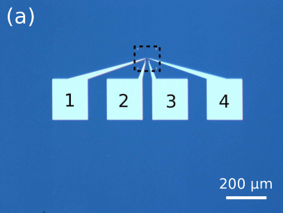
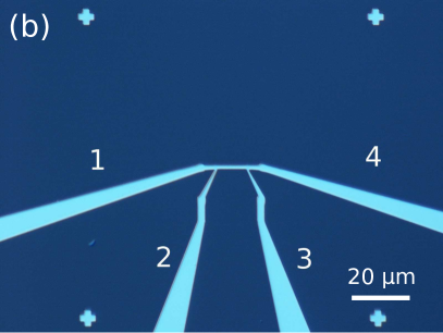
The heaters used in our research are manufactured by electric beam (e-beam) lithography to ensure that their shape is well defined. A Si/SiO2 (100 nm oxide) substrate is coated with a negative e-beam resist. The heaters are patterned in the resist and the part exposed to the beam is developed away. The heaters, typically about 60 on each substrate chip, are deposited via sputtering where a 5 nm thick polycrystalline Cr adhesion layer is grown before the 50 nm polycrystalline Pt layer. The growth rate of Cr is 3.2 nm/min and that of the Pt is 5.2 nm/min. For further details on the film growth we refer to Au et al. (2008). A lift-off step in an acetone bath leaves us with the final structure. The chip is rinsed and then the heaters are ready for use. The dimensions of the microheaters used in this study are 110 m2, and their thickness is as detailed above. We have measured the surface roughness of our films by atomic force microscopy, and in all cases the rms roughness is below 1 nm. A typical microheater is depicted in fig. 1.
We use four terminal electrical measurements to obtain the power dissipation in our heaters, , as this enables us to have accurate control over the temperature of the heaters. We use a homemade circuit to both monitor and to regulate the power dissipation in the heater. This process is computer controlled via a programmable National Instruments Data Acquisition board (DAQ-board, NI-USB 6229). The setup and the circuit is thoroughly described in Elíasson et al. (2014). We subject our microheaters to a high current density, and wait until they eventually fail due to electromigration, in order to test their time-to-failure. By switching the current polarity at a frequency of kHz (referred to as AC current stress in the article) we observed on the order of 103-fold increase in the time-to-failure of our heaters, compared to when they are biased at the same power level at DCElíasson et al. (2014). Depending on the bias, our measurements can take quite some time, the longest measurement on a single heater lasted for over a week.
Three quantities describing the properties of our heaters are of special interest. These are their electrical resistance (in particular the cold resistance ), the thermal impedance and the temperature coefficient of resistance . Attempts were made to determine if any permanent changes occur in these quantities upon subjecting our heaters to high power. Our findings show that both and appear to be essentially unchanged despite thermal cycling, whether it be by varying the current density or by external heating (on a hotplate). However, we found that the heater resistance changes substantially in our samples and devote section III to discussion on those observations.
These properties, and , can be obtained by current-voltage (-) measurements, with the help of a hot plate to vary temperature, as follows: An as-grown heater is - characterized. These measurements result in a cold resistivity of
| (3) |
This value is about 90% greater than the bulk resistivity of PtKittel (1995), = 10.4 cm, but it should be kept in mind that this is a thin and narrow wire with large contribution to resistivity from surface scattering. Its - profile is stored likewise. In the linear part of the - graph the line is described by combining eqs. (1) and (2)
| (4) |
where is the power dissipated in the heater and is the resistance at mW.
The heater is now measured on a hot plate, whose temperature is increased stepwise and changes in resistance are observed. We measured over a temperature range from room temperature up to about 110∘C, and found from fitting eq. 2 to be
| (5) |
From the - graph the value of can now be estimated. For our heaters we obtained a value of
| (6) |
The heater is now subjected to constant high power (which is the quantity regulated) for a few minutes, a time long enough so an obvious decrease in the heaters resistance has been observed, see sec. III. Following this procedure the heater’s - profile is obtained again to measure the cold resistance and its value is measured again to see if it had changed. We found no changes in or as mentioned earlier. This is in agreement with results from Pt films annealed to temperatures of 1300∘CZhang et al. (1997).
All the heaters in our study are manufactured in the exact same manner, therefore we assume they have the same physical characteristics. We chose to regulate heater power at a value of mW in our measurements. This power value was obtained by trial and error, as heater failure is a statistical event. It was chosen such as to see a substantial decrease in in the first few minutes upon biasing and a “reasonable” time-to-failure. At this high power we estimate the temperature in light of eq. (1) and (6) as being K corresponding to about 440∘C.
III Monitoring resistance
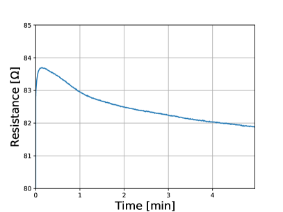
The effect of temperature on the resistance of a metal slab is well known and may be described by eq. (4). When subjected to high power, the resistance of our heaters rose during the first few seconds as can be expected due to self-heating, but when the desired regulation power (90 mW) was reached we noted a decrease in —steep at first but then with a gradually declining slope, as if the resistance follows an inverse power law. This can be seen in fig. 2, that shows an - (resistance-time) graph of an as-grown heater whose power was regulated at mW under AC current stress. In this particular measurement we ramped the heater power up slowly and then ramped it back down after 5 minutes of constant high power regulation. In ref. Elíasson et al., 2014 there can be found examples of measurements where after the drop, the resistance reaches a minimum, followed by a rise in the resistance leading to the eventual break of the heater due to electromigration.
This early drop in is also observed in as-grown heaters subjected to DC current stress. If the bias is maintained for long enough time the resistance typically starts to rise again and eventually the heater breaks due to electromigrationElíasson et al. (2014). Further, it appears to reflect an irreversible change in the sample properties, i.e. the material structure, as far as we can see.
An interesting effect can be seen in fig. 3 (a), which is an - graph of a heater where the power is ramped up at 1 mW/s. It compares the resistance during the first two ramp-ups, which are quite distinct. Later ramp-ups (the 3rd, 4th etc.) were almost identical to the second one, and thus omitted in the graph. During the first ramp-up there is a steep rise in the resistance at mW (power is maintained constant in 1 mW steps). This power value corresponds to a temperature of about 370∘C, according to eq. (1). We take this as a sign of permanent change in the heater’s material structure which seems to happen when its power is driven above a certain limit for the first time. A reduction in is caused by less electron scattering, which we attribute to growth in grain size of the polycrystalline Pt filmZhang et al. (2006); Wang et al. (2011).
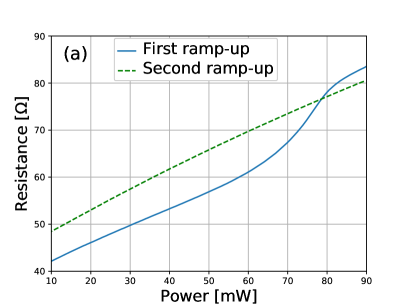
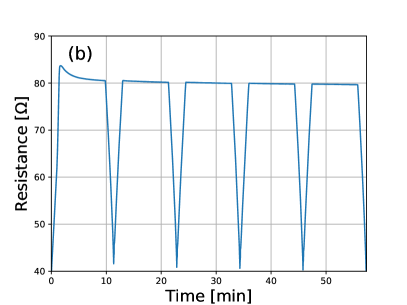
Fig. 3 (b) depicts an - graph of the same heater, again with the power ramped up at a rate of 1 mW/s. When the desired power is reached it is maintained for several minutes, and then lowered again (corresponding to the dips in resistance). This is repeated at regular intervals. As can be seen in the figure, the resistance trace reaches the same value after each ramp-up as it had prior to the ramp down of the power, further supporting the hypothesis of irreversible change to the sample.
Changes in , imply changes in the resistivity of the heater. Based on Matthiessen’s rule, we can simply add the contributions to the resistivity of a thin film , such that
| (7) |
Here is the bulk resistivity, a term caused by grain boundary scattering, comes from surface scattering and results from the surface roughness of the film. Wissmann and Finzel (2007) Our films are smooth compared to the thickness, so we can safely say that is very small and will not be considered here. According to the Fuchs-Sondheimer modelFuchs (1938); Sondheimer (1952) is a constant quantity for a constant value of the thickness of the metal film. We argue, based on measurements presented in the following section, that the main reason for the reduction in observed in fig. 2, is due to grain growth in the Pt film, which yields a decrement in .
IV Grain size measurements
In order to test the grain growth hypothesis we conducted two kinds of measurements to measure the grain size of the heaters and of Pt thin films grown in an identical manner to the ones our heaters are patterned from. We employ grazing incidence X-ray diffraction (GIXRD) measurements and scanning electron microscope (SEM) which give different information about the sample. GIXRD measurements are useful for polycrystalline thin films where the grains are randomly oriented. One also typically obtains better signal strength than in ordinary -2 measurements. It should be kept in mind that during GIXRD the incident X-rays are kept at a fixed low angle while the detector is scanned through a range of angles. As a result, the different peaks in the GIXRD scan represent different plane orientations (or -vector directions). While SEM imaging yields an estimate of , different GIXRD peaks can be used to obtain estimates of grain sizes in directions corresponding to the -vector orientation. Further, we compare the effect of running large electric current (high current density) in our samples with that of annealing identical thin films in an oven at various temperatures. As mentioned earlier the self heating at high current density raises the heater temperature quite significantly (440∘C at 90 mW power dissipation).
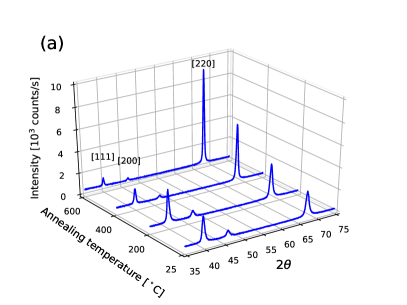
Our heater structures are too small to measure them directly in an X-ray apparatus. Thus four Cr/Pt films were grown in the same manner as the heaters, and three of these were post-annealed for 30 minutes at 200∘C, 400∘C and 600∘C temperature, respectively. The results of subsequent GIXRD measurements on all four films are presented in fig. 4 (a). Using the Scherrer equation, (crystalline coherence length), can be calculated in the following manner:Langford and Wilson (1978)
| (8) |
Here is the FWHM of the peaks in the GIXRD spectrum (three peaks were observed corresponding to crystalline planes [111], [200] and [220]), is the peak position in the spectrum, is the wavelength of the X-rays used and = 0.9 is the Scherrer correction factor. Scherrer’s equation is used to compare values of and observe trends, rather than for exact estimation of the grain size perpendicular to film plane. We graph the results in fig. 4 (b). Grain growth is apparent with increasing post-annealing temperature.
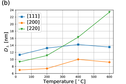
Similar measurements on Pt were not found in the literature, but in ref. Wissmann and Finzel, 2007, GIXRD measurements on thin Ag films are discussed. Those results are in many respects identical to ours. They were conducted at a lower temperature range from about 90 K, up to 500 K (see chapter 3 of ref. Wissmann and Finzel, 2007). In fig. 4 (b) we see that the [111] and [200] peaks yield slowly increasing values of , but appear not to undergo substantial changes. This is in accordance with ref. Wissmann and Finzel, 2007, where those peaks give a constant value of for the same temperatures as ours, from 300 K and up. In addition we also measure the peak corresponding to the [220] crystalline plane. These planes appear to grow substantially in the temperature range of our measurements, just as the [111] and [200] planes did on lower temperatures in ref. Wissmann and Finzel, 2007.
The [220] crystalline planes appears to dominate in the structure, since the intensity of the peak increases at the cost of the other two planes measured. One also sees on fig. 4 (a), that the intensity of the [220] diffraction peak starts to grow between 200∘C and 400∘C. We associate this change with the steep rise in electrical resistance occurring during the first ramp-up curve of fig. 3 (a), at a heater temperature of about 370∘C. This is an indication of changes in the material structure and at this temperature of 370∘C the activation energies for these processes have been reached.
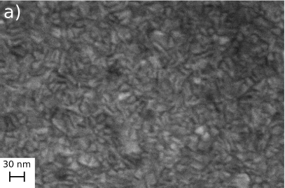
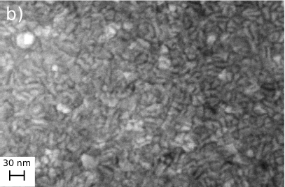
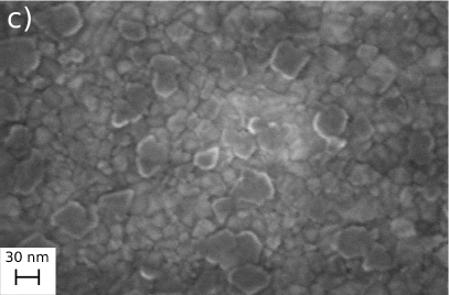
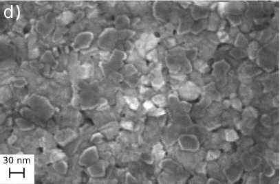
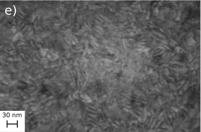
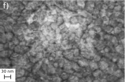
The in-plane grain size was also estimated in a SEM, see figs. 5 (a)–5 (f). Grain growth is apparent upon annealing. varies from about 15 nm for the unannealed film up to 30 nm for the the one annealed at C. In addition figs. 5 (e) and 5 (f) display the grain size of microheaters before and after electrical measurement at 90 mW constant power. The same grain growth happens when the heater is subjected to high current density which raises its temperature according to eq. 1. The material is annealed, just not in an oven but by self-heating. In addition one notices that not only the size of the grains changes, but also the shape. The grains appear to take on a rounder shape in contrast to the more oblong shape of the grains in the unannealed films. Similar growth of post-annealed thin Pt films is reported in ref. Agustsson et al., 2008.
V Conclusions
We investigated nm thick Pt microheaters of lateral dimensions 110 m2, subjected to current density up to about A/cm2. We regulate the electric power dissipated in the heater at a constant value of mW, obtained by trial and error, chosen to see a substantial decrease in . At this high power we estimate the temperature in light of eqs. (1) and (6) to be K, about 440∘C. As expected, by increasing the power dissipation in the microheater the resistance increases as described by eq. (4). When the desired regulation power was reached, the heater’s resistance drops, steeply at first but then the process slows down. The decrement in the heater resistance is permanent, which indicates a modification of the heaters’ structural properties. To investigate the structure of these heaters, we used two different techniques: SEM and GIXRD. From those measurements we see that the grains in thin Pt films start to grow when heated to temperatures between 200∘C and 400∘C. Indeed we also see signs of these structural changes in the heater when current is run through it the first time, then at heater temperature of about 370∘C. We conclude that the observed decrease in the heaters resistance, is due to grain growth in the metal as it is subjected to high electrical power.
Acknowledgements.
This work was partially supported by the Icelandic research fund.References
- Hamann, Lacey, and Ingvarsson (2008) H. F. Hamann, J. A. Lacey, and S. Ingvarsson, Journal of Microscopy 229, 512 (2008).
- Ottonello Briano et al. (2014) F. Ottonello Briano, P. Renoux, F. Forsberg, H. Sohlström, S. Ingvarsson, G. Stemme, and K. B. Gylfason, in SPIE Photonics Europe, edited by L. Vivien, S. Honkanen, L. Pavesi, S. Pelli, and J. H. Shin (SPIE, 2014) pp. 91331D–7.
- Ottonello Briano et al. (2016) F. Ottonello Briano, H. Sohlström, F. Forsberg, P. Renoux, S. Ingvarsson, G. Stemme, and K. B. Gylfason, Applied Physics Letters 108, 193106 (2016).
- Cvitkovic et al. (2006) A. Cvitkovic, N. Ocelic, J. Aizpurua, R. Guckenberger, and R. Hillenbrand, Phys. Rev. Lett. 97, 060801 (2006).
- Renoux et al. (2011) P. Renoux, S. Æ. Jónsson, L. J. Klein, H. F. Hamann, and S. Ingvarsson, Opt Express 19, 8721 (2011).
- Chan, Soljačić, and Joannopoulos (2006) D. L. C. Chan, M. Soljačić, and J. D. Joannopoulos, Opt Express 14, 8785 (2006).
- Black (1969) J. Black, IEEE Transactions on Electron Devices 16, 338 (1969).
- Gardner, Meindl, and Saraswat (1987) D. Gardner, J. Meindl, and K. Saraswat, IEEE Transactions on Electron Devices 34, 633 (1987).
- Liew, Cheung, and Hu (1989) B. Liew, N. Cheung, and C. Hu, in Reliability Physics Symposium, 1989. 27th Annual Proceedings., International (1989) pp. 215–219.
- Clement (2001) J. J. Clement, IEEE Transactions on Device and Materials Reliability 1, 33 (2001).
- Lloyd (1997) J. Lloyd, Semiconductor science and technology 12, 1177 (1997).
- Lloyd (1999) J. Lloyd, Journal of Physics D: Applied Physics 32, R109 (1999).
- Banerjee and Mehrotra (2001) K. Banerjee and A. Mehrotra, IEEE Circuits and Devices Magazine 17, 16 (2001).
- Ceric and Selberherr (2011) H. Ceric and S. Selberherr, Materials Science & Engineering R 71, 53 (2011).
- Ingvarsson et al. (2007) S. Ingvarsson, L. J. Klein, Y.-Y. Au, J. A. Lacey, and H. F. Hamann, Opt Express 15, 11249 (2007).
- Au et al. (2008) Y.-Y. Au, H. Skulason, S. Ingvarsson, L. Klein, and H. Hamann, Phys. Rev. B 78 (2008).
- Vasile, Arikan, and Ingvarsson (2012) G. Vasile, M. Arikan, and S. Ingvarsson, J. Phys. D: Appl. Phys. 45, 445106 (2012).
- Knobel et al. (1995) M. Knobel, P. Allia, C. Gomez-Polo, H. Chiriac, and M. Vazquez, Journal of Physics D: Applied Physics 28, 2398 (1995).
- Sossmeier et al. (2007) K. D. Sossmeier, F. Bohn, H. Chiriac, and M. Carara, Journal of Physics D: Applied Physics 40, 3233 (2007).
- Kholid et al. (2016) F. N. Kholid, H. Huang, Y. Zhang, and H. J. Fan, Nanotechnology 27, 025703 (2016).
- Jónsson (2009) S. Æ. Jónsson, Nonlinear Thermal Electric Analysis of Platinum Microheaters, Ph.D. thesis, University of Iceland (2009).
- Shatzkes and Lloyd (1986) M. Shatzkes and J. R. Lloyd, J. Appl. Phys. 59, 3890 (1986).
- Elíasson et al. (2014) O. Elíasson, G. Vasile, S. Æ. Jónsson, G. Gudjonsson, M. Arikan, and S. Ingvarsson, Review of Scientific Instruments 85, 114709 (2014).
- Kittel (1995) C. Kittel, Introduction to Solid State Physics, 7th ed. (John Wiley and sons, 1995).
- Zhang et al. (1997) J. Zhang, Y. Nagao, S. Kuwano, and Y. Ito, Japanese Journal of Applied Physics 36, 834 (1997).
- Zhang et al. (2006) Q. G. Zhang, X. Zhang, B. Y. Cao, M. Fujii, K. Takahashi, and T. Ikuta, Appl. Phys. Lett. 89, 114102 (2006).
- Wang et al. (2011) H.-D. Wang, J.-H. Liu, X. Zhang, Z.-Y. Guo, and K. Takahashi, Heat Mass Transfer 47, 893 (2011).
- Wissmann and Finzel (2007) P. Wissmann and H.-U. Finzel, Electrical Resistivity of Thin Metal Films (Springer Tracts in Modern Physics), 1st ed. (Springer, 2007).
- Fuchs (1938) K. Fuchs, Proc Cambridge Philos Soc (1938).
- Sondheimer (1952) E. H. Sondheimer, Advances in Physics 1, 1 (1952).
- Langford and Wilson (1978) J. Langford and A. Wilson, Journal of Applied Crystallography 11, 102 (1978).
- Agustsson et al. (2008) J. S. Agustsson, U. B. Arnalds, A. S. Ingason, K. B. Gylfason, K. Johnsen, S. Olafsson, and J. T. Gudmundsson, Applied Surface Science 254, 7356 (2008).