Origins of diamond surface noise probed by correlating single spin measurements with surface spectroscopy
Abstract
The nitrogen vacancy (NV) center in diamond exhibits spin-dependent fluorescence and long spin coherence times under ambient conditions, enabling applications in quantum information processing and sensing [1, 2]. NV centers near the surface can have strong interactions with external materials and spins, enabling new forms of nanoscale spectroscopy [3, 4, 5, 6]. However, NV spin coherence degrades within 100 nanometers of the surface, suggesting that diamond surfaces are plagued with ubiquitous defects [7, 8, 9, 10]. Prior work on characterizing near-surface noise has primarily relied on using NV centers themselves as probes [7, 8, 9, 10, 11, 12]; while this has the advantage of exquisite sensitivity, it provides only indirect information about the origin of the noise. Here we demonstrate that surface spectroscopy methods and single spin measurements can be used as complementary diagnostics to understand sources of noise. We find that surface morphology is crucial for realizing reproducible chemical termination, and use these insights to achieve a highly ordered, oxygen-terminated surface with suppressed noise. We observe NV centers within 10 nm of the surface with coherence times extended by an order of magnitude.
Sorawis Sangtawesin1,∗, Bo L. Dwyer2,∗, Srikanth Srinivasan1, James J. Allred1, Lila V. H. Rodgers1, Kristiaan De Greve2, Alastair Stacey3, Nikolai Dontschuk3, Kane M. O’Donnell4, Di Hu5, D. Andrew Evans5, Cherno Jaye6, Daniel A. Fischer6, Matthew L. Markham7, Daniel J. Twitchen7, Hongkun Park2,8, Mikhail D. Lukin2, Nathalie P. de Leon1
Department of Electrical Engineering, Princeton University, Princeton, NJ 08544, USA
Department of Physics, Harvard University, Cambridge, MA 02138, USA
Centre for Quantum Computation and Communication Technology, School of Physics, University of Melbourne, Parkville, VIC 3010, Australia
Department of Physics, Astronomy and Medical Radiation Science, Curtin University, Bentley, WA, Australia
Department of Physics, Aberystwyth University, SY23 3BZ Aberystwyth, UK
Material Measurement Laboratory, National Institute of Standards and Technology, Gaithersburg, MD 20899, USA
Element Six, Harwell OX11 0QR, UK.
Department of Chemistry and Chemical Biology, Harvard University, Cambridge, MA 02138, USA
These authors contributed equally to this work
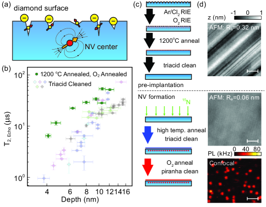
Although it is easy to place NV centers near the surface by low-energy ion implantation [8, 9] or delta-doping [7, 8], the surface itself can host defects that lead to noise that obscures the sensing target (Fig. 1a). We observe that coherence time degrades with proximity to the surface in numerous samples with different surface conditions (Fig. 1b), consistent with prior studies [7, 10], pointing to the need for new techniques to understand and control diamond surfaces. Gaining precise control over diamond surface chemistry is challenging because diamond is a chemically inert material, and also because it is hard to prepare uniform, flat diamond surfaces. Surface morphology is difficult to control because diamond’s hardness makes etching and polishing non-trivial. State-of-the-art diamond polishing can achieve surface roughness below 1 nm, but the resulting surface is highly strained. Plasma etching can remove this strained layer [13, 14], but this process is highly anisotropic and therefore small differences in initial conditions can lead to dramatic differences in final morphology and termination [15, 16] (see Supplementary Information). Therefore, direct characterization of the surface is crucial for establishing that particular protocols reproducibly lead to specific, desired surface terminations.
In this work, we characterize the diamond surface by correlating photoelectron spectroscopy, X-ray absorption, atomic force microscopy (AFM), and electron diffraction with measurements of NV spin decoherence and relaxation to identify and eliminate sources of noise at the surface. We find that surface roughness leads to poor NV coherence, and we observe that surface morphology changes the density of electronic defects observed with photoelectron spectroscopy, even for the same nominal chemical termination, implying that it is critical to maintain precise control over surface purity and morphology at every processing step.
In our procedure, we remove surface and subsurface damage resulting from polishing and reactive ion etching (RIE) before ion implantation, perform high-temperature annealing to remove implantation damage, and use oxygen annealing followed by wet oxidation to terminate the surface (see Methods). In order to ensure high purity throughout processing, samples are cleaned in a refluxing mixture of concentrated perchloric, nitric, and sulfuric acids (triacid clean) before RIE and all annealing steps. Starting with scaife-polished substrates with RMS roughness of less than 1 nm, we can typically achieve final oxygen-terminated surfaces with RMS roughness 100 pm, as measured by AFM (Fig. 1c). We show detailed examples in the Supplementary Information of contamination and irreversible surface roughening when this procedure is not followed. Using this surface processing, we extend the coherence times of NV centers within nanometers of the surface by around one order of magnitude (Fig. 1b).
To study the effects of different oxygen terminations on spin coherence, we prepare samples containing shallow NV centers using low-energy ion implantation followed by high-temperature annealing at 800∘C and triacid cleaning, and focus on detailed comparison before and after oxygen annealing. This procedure, excluding the final oxygen annealing step, is widely used for preparing shallow NV centers [3, 4, 7, 17, 11, 18]. We isolate the impact of the oxygen annealing step by studying the same NV centers near the surface through multiple processing cycles with and without this step.
We performed single spin measurements before and after oxygen annealing. Six NV centers were randomly selected from a confocal scan, and the direct comparison of their properties under the two surfaces is shown in Fig. 2. We measured the coherence time, , using a Hahn echo sequence for each NV center. We then studied the spectrum of the local magnetic field noise environment using XY4 and XY8 dynamical decoupling sequences [19, 9]. Additionally, we studied the high frequency spectral properties of the noise using single- and double-quantum relaxation measurements for both surfaces [20].
We observe a significant increase in under the oxygen-annealed surface compared to the triacid cleaned surface (Fig. 2a,c), indicating that noise at the surface is suppressed upon oxygen annealing. However, still decreases as the NV centers approach the surface, indicating that surface noise remains the dominant source of decoherence. Figure 2b shows an example of the measured coherence time, , as a function of the number of -pulses, . We observe a clear improvement in under the oxygen-annealed surface by up to a factor of four compared to the triacid-cleaned surface for all (see Supplementary Information). For a slowly fluctuating bath, such as 13C nuclear spins or dilute P1 center electron spins, is expected to scale as (Fig. 2b dashed lines) [19]. We fit the data to the scaling and obtain across all NV centers, and in some cases, we observe that saturates for (Fig. 2b, Supplementary Information). This deviation from the expected scaling indicates that the noise at the surface is broadband, and spectral decomposition reveals a noise spectrum spanning 10 kHz to 1 MHz (see Supplementary Information).
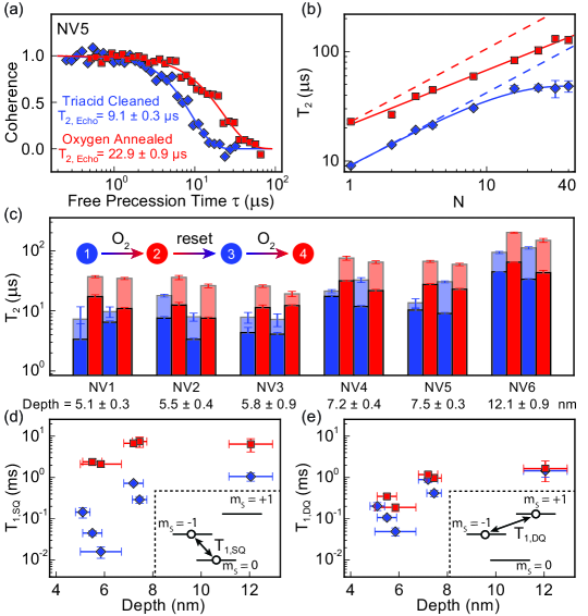
Because the surface morphology remains smooth through oxygen annealing (Fig. 1d), the termination is reversible. We demonstrate this reversibility by performing a “surface reset” via 800∘C vacuum annealing and triacid cleaning (Fig. 2c, inset). For direct comparison between different surfaces, we measure the coherence time with Hahn echo, , and XY8, , sequences from the same NV centers across different surface terminations. After the surface reset, coherence times are reduced to values comparable to those prior to oxygen annealing. Finally, these coherence times can be restored by repeating the oxygen annealing, showing that we have reproducible control over surface termination.
We note that we achieve the longest coherence times by annealing at 1200∘C after annealing at 800∘C (Fig. 1b). The higher temperature removes divacancies and multivacancy centers that form after ion implantation, which can contribute magnetic noise [21, 22, 10, 23]. However, we also observe that the NV center charge state is not stable after 1200∘C annealing without subsequent oxygen annealing. Therefore, to isolate the role of the oxygen termination, we have performed these experiments with only an 800∘C post-implantation anneal.
We probe the separate contributions of electric and magnetic noise by measuring relaxation rates between different levels in the NV ground state (Fig. 2d,e). The single-quantum (SQ) transition can be driven by magnetic noise, while the double-quantum (DQ) transition is magnetically forbidden and can thus be used to probe electric field noise. Comparison of the measured SQ and DQ spin relaxation times allows for the extraction of SQ and DQ transition rates, which are a reflection of the relative contributions of electric and magnetic noise [20]. Figure 2d shows the measured SQ and DQ spin relaxation times, and , measured at 40 G for the two different surface terminations. We observe an improvement in of 1-2 orders of magnitude after oxygen annealing, indicating that the high frequency magnetic field noise is strongly suppressed, consistent with measurements that probe the magnetic field noise at lower frequencies. In comparison, exhibits a small improvement (less than a factor of three) after oxygen annealing (Fig. 2e). Dynamical decoupling, SQ, and DQ relaxation measurements are sensitive to different frequency regimes, but the DQ transition rate is expected to scale inversely with frequency [20], allowing for extrapolation to other frequencies. Spectral comparison of the dynamical decoupling data and DQ relaxation data indicates that the electric field noise is not the dominant source that limits the coherence of NV centers under either surface termination (see Supplementary Information).
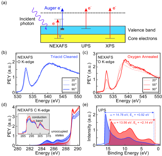
NV-based measurements indirectly suggest that the triacid-cleaned and oxygen-annealed surfaces have different electronic structure. To directly characterize the structure and chemical composition of the two different oxygen-terminated surfaces, we employ a variety of surface-sensitive spectroscopy techniques (Fig. 3a). Near-edge X-ray absorption fine structure spectroscopy (NEXAFS) probes the density of unoccupied states near the surface, ultraviolet photoelectron spectroscopy (UPS) gives information about the Fermi energy and electron affinity, and X-ray photoelectron spectroscopy (XPS) yields information about the chemical state of the surface termination.
The NEXAFS spectra at the oxygen K-edge for the two surfaces are qualitatively similar (Fig. 3b,c). Both exhibit a sharp peak at 532.5 eV and a broad shoulder at around 540 eV, indicating similar chemical states. Varying the angle of incidence of the linearly-polarized X-rays changes the relative polarization with respect to the surface normal. As this angle is varied, the signal changes dramatically for the oxygen-annealed surface (Fig. 3c), while the triacid-cleaned surface shows no variation (Fig. 3b). Strong polarization dependence arises from distinct and well-resolved bond orientations [24], indicating that the oxygen-annealed surface is highly ordered at the atomic scale, while the oxygen groups in the acid-cleaned surface are disordered (Fig. 4b).
The NEXAFS spectra at the carbon K-edge (Fig. 3d) show a characteristic exciton peak at 289.2 eV and a second absolute band gap at 302.2 eV [25]. At energies below the exciton peak at the conduction band edge, both surfaces exhibit two peaks, one at 285 eV that is assigned to carbon, and one at 286.5 eV associated with oxygen termination [25]. However, the triacid-cleaned surface has an average of 2.4 times higher density of unoccupied states below the conduction band edge, indicated by the area under the pre-edge region. These energetically deep unoccupied states at the surface can potentially act as electronic traps that host unpaired electrons, which can contribute both magnetic and electric field noise [26]. Furthermore, a morphologically rough surface after the same surface preparation and oxygen annealing exhibits a much larger density of unoccupied states than the smooth surface (see Supplementary Information). Using UPS, we observe that the oxygen-annealed surface exhibits a positive electron affinity of 2.14 eV, compared to 0.92 eV for the triacid-cleaned surface (Fig. 3e), indicating that the two surfaces possess drastically different electronic structure. To the best of our knowledge, this electron affinity is the largest reported for oxygen-terminated diamond [27].
Combining the data from surface spectroscopy and NV measurements, we conclude that disorder at the surface can lead to unoccupied defect states near the conduction band edge of diamond, which in turn lead to rapid decoherence of NV centers near the surface. These defect states give rise to broadband magnetic noise that cannot be circumvented by simple dynamical decoupling. It is therefore important for future applications in nanoscale sensing to devise methods to eliminate disorder and defect states at the diamond surface.
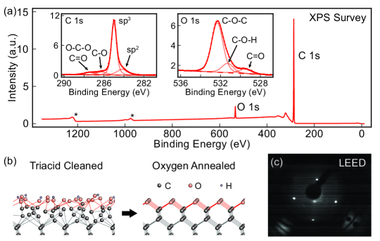
We now turn our attention to the chemical identification of the well-ordered, oxygen-annealed surface. XPS (Fig. 4a) reveals that the only detectable atoms are carbon and oxygen. The oxygen peak comprises 6–7% of the signal, corresponding to approximately monolayer surface coverage (see Supplementary Information). High-resolution XPS was used to probe the structure of the carbon and oxygen peaks in detail (Fig. 4a, inset). The carbon spectrum shows a dominant peak at 285 eV, which we assign to diamond carbon. Two satellite peaks at higher binding energies of +1.2 eV and +2.4 eV correspond to carbon singly- and doubly-bonded to oxygen, respectively [28]. The peak at lower binding energy of -0.8 eV is assigned to carbon. The oxygen spectrum shows a major peak at 532.3 eV and two satellite peaks at lower binding energies of -1.0 eV and -2.8 eV with a relative ratio of 10:1:1. These peaks have been previously assigned to ether, alcohol, and ketone, respectively [29]. Low-energy electron diffraction (LEED) indicates that the surface is reconstructed (Fig. 4c). Combining the XPS and LEED data, we assign the surface as predominantly ether-terminated (90%), with a minority mixture of alcohol and ketone groups (Fig. 4b). Additionally, our measured electron affinity is consistent with density functional theory calculations of an ether-terminated surface [30]. We note that all of the surface spectroscopy techniques are unable to directly detect hydrogen, and we thus cannot exclude that the mixed surface includes residual hydrogen, although the large positive electron affinity rules out significant hydrogen incorporation [27].
While the coherence of shallow NV centers is significantly improved by the techniques presented here, these coherence times remain far from typical bulk values [31]. The present work suggests a number of promising avenues for future study. The peak observed in NEXAFS and XPS is a deep electronic trap, and is a natural target for improvement [26]. It was also recently demonstrated that NV center coherence can be improved by implanting nitrogen through a boron-doped layer [10]. Combining such strategies with our surface preparation could yield even longer spin coherence. Finally, it is unknown what contribution adventitious carbon contamination makes to magnetic and electric field noise. Our on-going work includes preparing and interrogating surfaces in ultrahigh vacuum conditions to disentangle the contributions of chemical surface termination and exogenous contamination.
Our approach of combining surface spectroscopy with single spin measurements can be applied to the future development of novel surface terminations. We have shown that surface morphology and electronic structure measurements can help to evaluate which surfaces are likely to lead to further improvements in NV coherence, which can provide useful benchmarking for rapid exploration of new surface chemistry. More broadly, the strategy of correlating surface spectroscopy with qubit measurements can be applied to a variety of quantum platforms that also exhibit deleterious effects from surfaces and interfaces, such as superconducting qubits [32], trapped ions [33], and shallow donors [34].
References
- [1] Maze, J. R. et al. Nanoscale magnetic sensing with an individual electronic spin in diamond. Nature 455, 644–647 (2008).
- [2] Dobrovitski, V. V., Fuchs, G. D., Falk, A. L., Santori, C. & Awschalom, D. D. Quantum control over single spins in diamond. Annu. Rev. Condens. Matter Phys. 4, 23 (2013).
- [3] Staudacher, T. et al. Nuclear Magnetic Resonance Spectroscopy on a (5-Nanometer)3 Sample Volume. Science 339, 561–563 (2013).
- [4] Mamin, H. J. et al. Nanoscale Nuclear Magnetic Resonance with a Nitrogen-Vacancy Spin Sensor. Science 339, 557–560 (2013).
- [5] Grinolds, M. S. et al. Subnanometre resolution in three-dimensional magnetic resonance imaging of individual dark spins. Nature Nanotech. 9, 279–284 (2014).
- [6] Glenn, D. R. et al. High-resolution magnetic resonance spectroscopy using a solid-state spin sensor. Nature 555, 351 (2018).
- [7] Myers, B. A. et al. Probing surface noise with depth-calibrated spins in diamond. Phys. Rev. Lett. 113, 027602 (2014).
- [8] Rosskopf, T. et al. Investigation of surface magnetic noise by shallow spins in diamond. Phys. Rev. Lett. 112, 147602 (2014).
- [9] Romach, Y. et al. Spectroscopy of Surface-Induced Noise Using Shallow Spins in Diamond. Phys. Rev. Lett. 114, 017601 (2015).
- [10] Fávaro de Oliveira, F. et al. Tailoring spin defects in diamond by lattice charging. Nat. Commun. 8, 15409 (2017).
- [11] Lovchinsky, I. et al. Nuclear magnetic resonance detection and spectroscopy of single proteins using quantum logic. Science 351, 836–841 (2016).
- [12] Kim, M. et al. Decoherence of Near-Surface Nitrogen-Vacancy Centers Due to Electric Field Noise. Phys. Rev. Lett. 115, 087602 (2015).
- [13] Thoms, B. D., Owens, M. S., Butler, J. E. & Spiro, C. Production and characterization of smooth, hydrogen- terminated diamond C(100). Appl. Phys. Lett. 65, 2957–2959 (1994).
- [14] Friel, I. et al. Control of surface and bulk crystalline quality in single crystal diamond grown by chemical vapour deposition. Diamond Relat. Mater. 18, 808–815 (2009).
- [15] Howe, J. Y., Jones, L. E. & Coffey, D. W. The evolution of microstructure of CVD diamond by oxidation. Carbon 38, 931 (2000).
- [16] Wolfer, M. et al. Crystallographic anisotropy of growth and etch rates of CVD diamond. Diamond Relat. Mater. 18, 713 (2009).
- [17] Sushkov, A. O. et al. Magnetic Resonance Detection of Individual Proton Spins Using Quantum Reporters. Phys. Rev. Lett. 113, 197601 (2014).
- [18] Pham, L. M. et al. NMR technique for determining the depth of shallow nitrogen-vacancy centers in diamond. Phys. Rev. B 93, 045425 (2016).
- [19] de Lange, G., Wang, Z. H., Ristè, D., Dobrovitski, V. V. & Hanson, R. Universal Dynamical Decoupling of a Single Solid-State Spin from a Spin Bath. Science 330, 60–63 (2010).
- [20] Myers, B. A., Ariyaratne, A. & Jayich, A. B. Double-Quantum Spin-Relaxation Limits to Coherence of Near-Surface Nitrogen-Vacancy Centers. Phys. Rev. Lett. 118, 197201 (2017).
- [21] Twitchen, D. J., Newton, M. E., Baker, J. M., Anthony, T. R. & Banholzer, W. F. Electron-paramagnetic-resonance measurements on the divacancy defect center in diamond. Phys. Rev. B 59, 12900 (1999).
- [22] Chu, Y. et al. Coherent Optical Transitions in Implanted Nitrogen Vacancy Centers. Nano Lett. 14, 1982–1986 (2014).
- [23] Yamamoto, T. et al. Extending spin coherence times of diamond qubits by high-temperature annealing. Phys. Rev. B 88, 075206 (2013).
- [24] Stöhr, J. NEXAFS Spectroscopy, vol. 25 of Springer Series in Surface Sciences (Springer Berlin Heidelberg, Berlin, Heidelberg, 1992).
- [25] Shpilman, Z. et al. A near edge X-ray absorption fine structure study of oxidized single crystal and polycrystalline diamond surfaces. Diamond Relat. Mater. 45, 20–27 (2014).
- [26] Stacey, A. et al. Evidence for primal defects at the diamond surface: Candidates for electron trapping and noise sources (2018). arXiv:1807.02946.
- [27] Maier, F., Ristein, J. & Ley, L. Electron affinity of plasma-hydrogenated and chemically oxidized diamond (100) surfaces. Phys. Rev. B 64, 165411 (2001).
- [28] Kitagawa, F. et al. XPS and NEXAFS studies of VUV/O3-treated aromatic polyurea and its application to microchip electrophoresis. IET Nanobiotechnol. 5, 136–142 (2011).
- [29] Baldwin, C. G., Downes, J. E., McMahon, C. J., Bradac, C. & Mildren, R. P. Nanostructuring and oxidation of diamond by two-photon ultraviolet surface excitation: An XPS and NEXAFS study. Phys. Rev. B 89, 195422 (2014).
- [30] Sque, S. J., Jones, R. & Briddon, P. R. Structure, electronics, and interaction of hydrogen and oxygen on diamond surfaces. Phys. Rev. B 73, 085313 (2006).
- [31] Balasubramanian, G. et al. Ultralong spin coherence time in isotopically engineered diamond. Nature Mater. 8, 383–387 (2009).
- [32] Gao, J. et al. Experimental evidence for a surface distribution of two-level systems in superconducting lithographed microwave resonators. Appl. Phys. Lett. 92, 152505 (2008).
- [33] Hite, D. et al. Surface science for improved ion traps. MRS Bulletin 38, 826–833 (2013).
- [34] Paik, S.-Y., Lee, S.-Y., Baker, W. J., McCamey, D. R. & Boehme, C. and spin relaxation time limitations of phosphorous donor electrons near crystalline silicon to silicon dioxide interface defects. Phys. Rev. B 81, 075214 (2010).
- [35] Gaebel, T. et al. Size-reduction of nanodiamonds via air oxidation. Diamond Relat. Mater. 21, 28–32 (2012).
- [36] Barr, T. L. & Seal, S. Nature of the use of adventitious carbon as a binding energy standard. Journal of Vacuum Science & Technology A 13, 1239–1246 (1995).
- [37] Watts, B. & Ade, H. A simple method for determining linear polarization and energy calibration of focused soft X-ray beams. Journal of Electron Spectroscopy and Related Phenomena 162, 49–55 (2008).
- [38] Williams, G. T. et al. High temperature photoelectron emission and surface photovoltage in semiconducting diamond. Appl. Phys. Lett. 105, 061602 (2014).
- [39] Wang, Z.-H., de Lange, G., Ristè, D., Hanson, R. & Dobrovitski, V. V. Comparison of dynamical decoupling protocols for a nitrogen-vacancy center in diamond. Phys. Rev. B 85, 155204 (2012).
0.1 Samples
In this letter, we present NV coherence data from several samples in Fig. 1b. Here, we describe the different samples:
-
•
Sample A: The sample used for data in Fig. 2. Commercially available electronic grade diamond (Element Six) with 5 ppb nitrogen and 1 ppb boron.
- •
-
•
Sample C: Another sample that originated from the same crystal as sample A. The crystal was sliced prior to any processing described in Fig. 1c.
-
•
Sample D: An electronic grade sample with 12C-enriched layer that was processed according to Fig. 1c.
-
•
Sample E: An electronic grade sample with 12C-enriched layer with rough, as-grown surface that was subsequently processed with Ar/Cl2 and O2 RIE.
-
•
Sample F: An electronic grade sample with 12C-enriched layer. The surface is left as-grown.
In addition to these NV samples, surface spectroscopy data is presented from several electronic grade samples. Three triacid-cleaned samples and three oxygen-high-resolutionannealed samples, one of which is morphologically rough, were used for NEXAFS and high-resolution XPS (Fig. 3b–d, Fig. 4a, inset). A boron doped sample (0.1 ppm boron and 5 ppb nitrogen) was used for UPS spectroscopy (Fig. 3e) to prevent charging. Finally, a lower purity sample (1 ppm nitrogen and 0.5 ppm boron, Element Six ”standard grade”) was used for oxygen annealing calibration.
0.2 Sample Preparation
Our method for preparing a high quality diamond surface prior to ion implantation relies on a multi-step process to remove surface and subsurface damage. Unless indicated otherwise, all samples described above are laser cut and scaife-polished to a RMS roughness of less than 1 nm with a major face and edges, specified to within 3∘. In order to prepare substrates for implantation, reactive ion etching was performed using an inductively coupled plasma (ICP) with the following parameters: 400 W ICP power, 250 W substrate bias RF power, 25 sccm Ar, 40 sccm Cl2, 8 mTorr for 30 minutes followed by 700 W ICP, 100 W substrate bias, 30 sccm O2, 10 mTorr for 25 minutes (Plasma-Therm Versaline ICP RIE). These two RIE steps etch approximately 2 and 4 of the subsurface polish damage layer, respectively [14].
In order to remove residual subsurface damage from ICP RIE, 1200∘C vacuum annealing is performed in a Lindberg Blue tube furnace with high purity (99.5%) alumina ceramic tubes at pressures between Torr and Torr with the following sequence, starting from room temperature:
-
1.
Ramp to 100∘C over 1 hour. Hold for 11 hours.
-
2.
Ramp to 400∘C over 4 hours. Hold for 8 hours.
-
3.
Ramp to 800∘C over 6–12 hours. Hold for 8 hours.
-
4.
Ramp to 1200∘C over 6–12 hours. Hold for 2 hours.
-
5.
Let cool to room temperature.
This annealing results in a 3 nm layer of amorphous carbon at the surface, which is subsequently removed by cleaning the sample in a refluxing 1:1:1 mixture of concentrated sulfuric, nitric, and perchloric acids (triacid clean) for at least one hour. The conversion of material to amorphous carbon and subsequent removal is critical for removing subsurface damage resulting from RIE processing. Annealing at lower pressures (below Torr) does not result in a thick layer of amorphous carbon, and thus does not remove this damage layer (see Supplementary Information).
Sample A was then sent for 15N ion implantation (Innovion) with the recipe: dose , energy 3 keV, and 0∘ tilt. Other samples were implanted with the same parameters, except with doses of for samples B and F and for samples C, D, and E. Following implantation, all samples are triacid cleaned and 800∘C annealed in vacuum using the same recipe as above, with or without the 1200∘C step. Another triacid clean following this vacuum anneal results in the condition referred to as the “triacid cleaned” surface throughout the text.
To create the oxygen-terminated surface, the sample is then annealed at 445–450∘C in a tube furnace (Lindberg Blue Mini-Mite with high-purity quartz process tube) under continuous flow of O2 at atmospheric pressure for 4 hours. The oxygen flow is regulated with a mass flow controller, and the outlet of the process tube is connected to a bubbler to prevent backflow of gases. The input gases, oxygen (for annealing) and nitrogen (for venting the furnace), are filtered via SAES Sentrol point-of-use purifiers, MC1-203F and MC1-902F, respectively. Following the oxygen anneal, the sample is cleaned in a 1:2 mixture of hydrogen peroxide in concentrated sulfuric acid (“piranha”). The resulting sample condition is referred to as the “oxygen-annealed” surface throughout the text. Finally, Sample B was annealed at 1200∘C and subsequently oxygen annealed to achieve the best spin coherence times, shown in Fig. 1b.
XPS is used between each step to verify that the surface is contamination free at the level, which is the sensitivity limit of the instrument. If any heteroatoms other than C and O are found (e.g. Na, Cl, Si), the sample is repeatedly cleaned with either triacid or piranha until the contamination is eliminated. In the Supplementary Information, we show examples of XPS spectra from a contaminated sample before and after acid cleaning, as well as micromasking and surface roughening that can result from contamination.
0.3 Process Calibration for Oxygen Annealing
Since diamond etches when heated in an oxygen atmosphere [35], changing the surface termination while avoiding etching requires careful temperature calibration. Our process proceeds as follows:
-
1.
Clean sample in 1:2 hydrogen peroxide in sulfuric acid (piranha). Verify that the sample is contaminant-free in XPS.
-
2.
In the furnace, ramp to the target temperature over 4 hours, and anneal at the target temperature for another 4 hours.
-
3.
Repeat step 1.
-
4.
Examine the sample in AFM to check for morphological changes at the surface.
-
5.
Cycle back to first step and increase target temperature.
Previous studies showed that diamond starts to etch in oxygen around 500∘C [35]. Therefore, we begin with 450∘C for our calibration and choose the final temperature to be the highest temperature that does not produce pitting on the sample. Examples of AFM images taken after annealing at different temperatures are shown in the Supplementary Information.
0.4 XPS and AFM Characterization
XPS survey scans in Fig. 4a and AFM images in Fig. 1c were performed at the Imaging and Analysis Center (IAC) at Princeton University. XPS was performed with a Thermo Fisher K-Alpha spectrometer, collecting photoelectrons normal to the surface. AFM was performed interchangeably with either a Bruker Nanoman or a Bruker ICON3 AFM operating in AC tapping mode (AFM tip: Asylum Research AC160TS-R3, resonance frequency 300 kHz). Each diamond was thoroughly cleaned with either triacid or piranha before AFM scans were performed. Large-scale ( m) and small-scale ( m or m) scans were performed in several distinct areas of the diamonds, away from the edge. In general, for the same sample, no clear variation of the RMS roughness was observed across the interrogated areas.
0.5 NEXAFS and High-Resolution XPS
In near-edge X-ray absorption fine structure spectroscopy (NEXAFS), monochromatic X-rays excite core electrons, and secondary electron yield is measured as a function of the incident X-ray energy, giving a signal that is proportional to the density of unoccupied states near the surface. In XPS, incident X-rays ionize core electrons, and the measured binding energy is sensitive to the chemical environment of the ionized atom.
Unless indicated otherwise, all NEXAFS data and high-resolution XPS spectra (Fig. 4 insets) in the main text and Supplementary Information were acquired at the Australian Synchrotron soft X-ray spectroscopy beamline, using light from an APPLE II undulator generating linearly polarized photons and passed through a plane-grating monochromator. Prior to scanning, the samples were annealed in situ at at 430∘C to remove adventitious carbon [36].
Carbon K-edge and oxygen K-edge NEXAFS were collected in partial electron yield mode with grid biases of 220 V and 440 V, respectively. The spectra are processed and calibrated by first dividing by the total incident power measured using photoelectrons from clean gold foil in the chamber, subtracting the average pre-edge background (270–275 eV for carbon, 520–525 eV for oxygen), and normalizing to the post-edge electron yield (315–320 eV for carbon, 558–560 eV for oxygen). The energy is calibrated by setting the sharp * exciton peak of the gold foil to 291.65 eV [37].
High-resolution XPS spectra were analyzed using a SPECS Phoibos 150 hemispherical analyzer with the pass energy set to 5 eV, resulting in a linewidth of better than 0.1 eV. An excitation photon energy of 600 eV was used. XPS spectra were fitted using CasaXPS. A linear fit to the pre-edge was first subtracted from the data to account for the rising secondary electron tail apparent in spectra acquired with a photon energy close to the core level energy. Subsequently, a universal Tougaard background was subtracted and Voigt functions were used to fit the resulting spectra. Each component function was constrained to have the same FWHM as all others within the same spectrum. We find that the carbon signal fit residual is minimized by fitting two side peaks on the high binding energy side rather than one, and that it does not improve by fitting three side peaks. We identify these two peaks as carbon singly- and doubly-bonded to oxygen.
0.6 Additional XPS, UPS, and LEED Measurements
Additional XPS (Supplementary Information), UPS, and LEED measurements were carried out in a custom UHV spectrometer at Aberystwyth University. X-ray excitation was provided by a VG twin-anode (Mg and Al) source and He I UV radiation was provided by a SPECS UVS 300 source. Photoelectrons were collected at normal emission by a SPECS Phoibos 100 analyzer using a 2D CCD electron detector.
In UPS, ultraviolet photons (21.2 eV) ionize valence electrons, and their binding energy can then be used to determine the Fermi energy and electron affinity. For XPS, the sample was kept at earth potential while for UPS, a bias of V was applied to the sample to enable collection of low energy electrons over a range of sample work functions. The electron analyzer was operated in wide angle mode to sample band edge states averaged in momentum space. Since the apparent binding energy of electron states measured by photoelectron spectroscopy is affected by surface charging and photovoltage generation [38], we calibrate the valence band edge against the Fermi edge of a tantalum standard. Rear-view VG LEED optics were used to record surface electron diffraction patterns. The beam energy was set to 86 eV for the diffraction pattern shown in Fig. 4c.
0.7 NV Measurement Setup
NV measurements were performed on a home-built confocal microscope. NV centers are excited by a 532 nm optically pumped solid state laser (Coherent Sapphire LP 532-300), which is modulated with an acousto optic modulator (Isomet 1205C-1). The beam is scanned using galvo mirrors (Thorlabs GVS012) and projected into an oil immersion objective (Nikon, Plan Fluor 100, ) with a telescope in a configuration. Laser power at the back of the objective was kept between 60–100 W, approximately of the saturation power of a single NV center, in order to avoid irreversible photobleaching. A dichroic beamsplitter (Thorlabs DMLP567) separates the excitation and collection pathways, and fluorescence is measured using a fiber-coupled avalanche photodiode (Excelitas SPCM-AQRH-44-FC). A neodymium magnet is used to introduce a DC magnetic field for Zeeman splitting, and the orientation of the magnetic field was aligned to within 1∘ of the NV axis using a combination of a rotation stage and a goniometer.
Spin manipulation on the NV center was accomplished using microwaves generated by a dual-channel signal generator (R&S SMATE200A). The two channels are independently gated with fast SPDT switches (Mini-Circuits ZASWA-2-50DR+) and combined with a resistive combiner (Mini-Circuits ZFRSC-42-S+) for double-quantum measurement capability. The combined signal is then amplified with a high-power amplifier (Mini-Circuits ZHL-16W-43+) and delivered to the sample via a coplanar stripline. The stripline is fabricated by depositing 10 nm Ti, 1000 nm Cu, and 200 nm Au on a microscope coverslip. Following metallization, the stripline is photolithographically defined and etched with gold etchant and hydrofluoric acid. Finally, a 100 nm layer of Al2O3 is deposited on top of the fabricated stripline via atomic layer deposition (ALD) to protect the metal layer. This Al2O3 layer is crucial for separating the diamond surface from the metal layer of the stripline, which can contaminate the diamond surface (see Supplementary Information). Pulse timing is controlled with a Spincore PulseBlaster ESR-PRO500 with 2 ns timing resolution, and phase control of the NV microwave pulses is achieved with an arbitrary waveform generator (Agilent 33622A). Hahn echo experiments were performed at to average out the free precession of the 1.1% natural abundance of 13C in the sample.
To avoid effects of pulse errors during dynamical decoupling, we alternate the phase of each -pulse using the XY4 protocol for the 4-pulse sequence, the XY8 protocol for the 8-pulse sequence, and repeated XY8 protocol for higher order sequences [39].
NV depths were measured by placing a drop of microscope immersion oil (Nikon NF2) on the surface and measuring the proton NMR signal arising from the oil [18].
We thank Adam Gali, Joseph Tabeling, and Jim Butler for numerous discussions about diamond surfaces, Nan Yao, Yao-Wen Yeh, and John Schreiber at the Princeton Imaging and Analysis Center for help with diamond surface characterization, Hans Bechtel and David Kilcoyne at the Advanced Light Source as well as Arthur Woll at the Cornell High Energy Synchrotron Source for advice about surface spectroscopy techniques, and Jeff Thompson for other fruitful discussions. This work was supported by the NSF under the CAREER program (grant DMR-1752047) and through the Princeton Center for Complex Materials, a Materials Research Science and Engineering Center (grant DMR-1420541). JJA acknowledges support from the National Science Foundation Graduate Research Fellowship Program, and LVHR acknowledges support from the Department of Defense through the National Defense Science and Engineering Graduate Fellowship Program. AS and ND acknowledge support from the Australian Research Council (CE170100012). Part of this research was undertaken on the Soft X-ray spectroscopy beamline at the Australian Synchrotron, part of ANSTO.
The authors declare that they have no competing financial interests.
Correspondence and requests for materials should be addressed to npdeleon@princeton.edu.