Direct observation of the CVD growth of monolayer MoS2 using in-situ optical spectroscopy
Abstract
Real-time monitoring is essential for understanding and eventually precise controlling of the growth of two dimensional transition-metal dichalcogenides (2D TMDCs). However, it is very challenging to carry out such kind of studies on chemical vapor deposition (CVD). Here, we report the first real time in-situ study on the CVD growth of the 2D TMDCs. More specifically, CVD growth of molybdenum disulfide (MoS2) monolayer on sapphire substrates has been monitored in-situ using differential transmittance spectroscopy (DTS). The growth of the MoS2 monolayer can be precisely followed by looking at the evolution of the characteristic optical features. Consequently, a strong correlation between the growth rate of MoS2 monolayer and the temperature distribution in the CVD reactor has been revealed. Our result demonstrates the great potential of the real time in-situ optical spectroscopy for the realization of the precisely controlled growth of 2D semiconductor materials.
Keywords: chemical vapor deposition (CVD); two dimensional transition-metal dichalcogenides (2D TMDC); molybdenum disulfide (MoS2) monolayer; in-situ differential optical spectroscopy.
1 Introduction
The two-dimensional transition metal dichalcogenides (2D TMDCs) have drawn wide attention because of their fascinating physical and chemical properties [1, 2, 3, 4, 5, 6]. Given that the potential advantages of 2D TMDCs as the active materials for various devices have been established, the primary requirement is cost-efficient, reliable, and high throughput synthesis of 2D TMDCs with processes compatible with the current semiconductor technology. Various approaches for synthesizing large-area 2D TMDCs have been reported, including mechanical exfoliations, sulphurization of metal thin films, mass transport, molecular beam epitaxy (MBE) and chemical vapor deposition (CVD) [6, 7]. In particular, CVD is considered as an attractive and very promising approach for large-scale synthesis of 2D TMDCs [8, 9, 10, 11, 12, 13, 14]. As a result, numerous empirical attempts have been taken to optimize the CVD process by choosing appropriate precursors, supporting substrate, carrier gases, flow rates, synthesis temperature, etc. Although these studies have created helpful growth recipes and inspired many theoretical discussions about the growth mechanisms, they were still unable to provide a clear path to the fully understanding of the growth mechanisms [10, 15, 16, 17, 18, 19]. Most recent efforts aiming at manipulating the nucleation and growth of 2D TMDCs have successfully led to the great improvement of the film quality and well orientated MoS2 monolayer has even been fabricated in wafer scale [12, 14, 16, 19]. These results highlight the important role of surface kinetics in the CVD growth of the 2D TMDCs. To improve our understanding on the surface kinetics involved, in-situ study performed during the CVD growth of 2D TMDCs is essential. However, according to the best of our knowledge, no study in this direction has been reported despite of its importance. Consequently, the growth mechanisms are still the subject of much speculation.
Because typical CVD used for the synthesis of 2D TMDCs involving gases with pressure in the range between atmosphere and hundredth of mbar, the characterization methods based on electron beam are not applicable and the in-situ real time study becomes very challenging. On the other hand, each kind of 2D TMDCs possess specific optical properties which are characteristic of their chemical composition, crystalline structure and number of layers [2, 20]. Their optical properties are also sensitive to the extrinsic modifications, for instance, interaction with substrate [21], gas molecule adsorption [22, 23] as well as strain field [24]. These facts make the optical spectroscopy a sensitive probe to the surface kinetics involved during the growth of 2D TMDCs. Furthermore, the optical methods in visible range can be applied under various environments including vacuum, atmosphere and even high pressure condition. Consequently, the optical spectroscopy is the method of choice for in-situ studies during the CVD growth. Monitoring the evolution of the optical properties of 2D TMDCs during CVD growth may provide a sensitive access to the surface processes and a characterization of morphology, crystalline structure of the films. By systematic study using in-situ optical spectroscopy assisted with other ex-situ characterizations, the details of the kinetics including adsorption, dissociation, reaction, nucleation and growth can be revealed.
Differential reflectance spectroscopy (DRS), which measures the normalized difference between the reflectance of the bare surface and the one covered by thin films, posses enhanced sensitivity to the surface modification and ultrathin film growth [25, 26]. The technique has been successfully applied to reveal the optical properties of 2D TMDCs [2, 20] and, most recently, also to monitor the molecular beam epitaxy of MoSe2 monolayer on sapphire substrate [27]. In the current work, we have applied an analogous technology, namely, differential transmittance spectroscopy (DTS), to realize in-situ real time study of the CVD growth of MoS2 monolayer on Al2O3(0001) surface. In this case, the normalized differences between the transmittance through the bare substrate and the one after a given deposition time are resolved. By monitoring the DTS during growth, the evolution of the optical properties associated to the MoS2 layer can be revealed spectroscopically. Actually, for the van der Waals epitaxy of MoS2 on the transparent sapphire substrate, the DT spectrum can be directly associated to the absorption of the adlayer. Consequently, the growth can be monitored in-situ in real time and the detailed information associated to the kinetics can be deduced from the DT spectra.
2 Results and Discussions
2.1 Ex-situ characterization
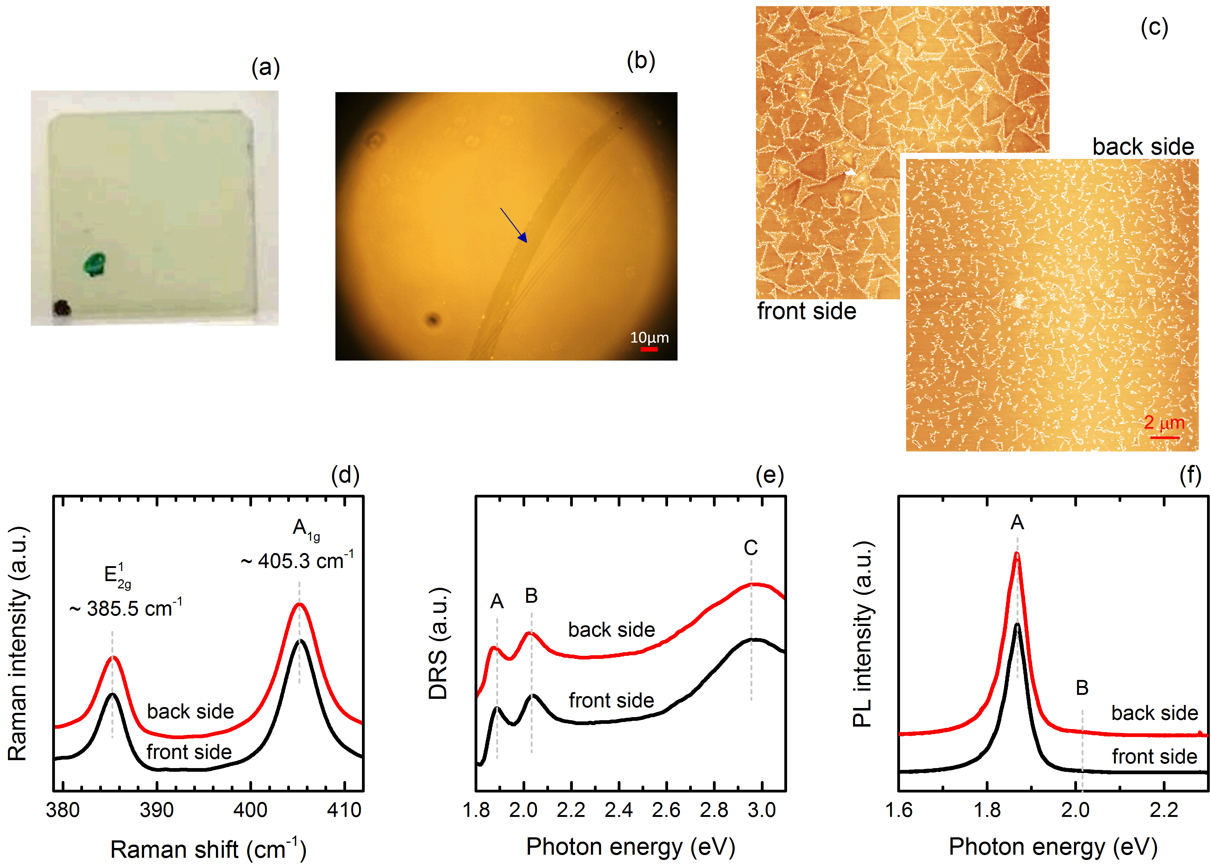
Following the CVD process described in the Experimental section, MoS2 monolayer has been deposited, simultaneously, on not only the surface at the front side (face to the Ar flow direction) but also the one at the back side of the sapphire substrate. This conclusion is based on a thorough ex-situ characterization after CVD growth using differential reflectance spectroscopy (DRS), Raman spectroscopy, photoluminescent spectroscopy (PL), optical microscopy (OM) and atomic force microscopy (AFM). Actually, from the first glance at the substrate after CVD (see Fig. 1(a)), it can be recognized that the substrate shows a homogeneous light green colour which is characteristic for the sapphire substrate covered by MoS2 monolayer. Indeed, OM images (Fig. 1(b)) taken at different areas of the front and back sides of the substrate reveal that the surfaces at both sides are covered by homogeneous layers which can only be recognized at the appearance of defects. Fig. 1(c) presents the AFM images measured at front and back sides of the sapphire substrate confirming both surfaces are covered by an almost completed monolayer of MoS2. The Raman spectra recorded from each side of the substrate (Fig. 1(d)) show the characteristic peaks at 385.5 and 405.3 cm-1, which are attributed to the in-plane (E) and out-of-plane (A1g) vibration mode of the 2H MoS2 crystal. Most importantly, the interval between these two peaks is 20 cm-1, which is characteristic for the MoS2 monolayer [28]. The DR spectra measured at the surfaces on the front and back sides of the substrate are plotted in Fig. 1(e). The peaks marked by A and B, which are located around 1.9 and 2 eV, are due to the excitonic transitions occurring at the K and K′ points of the Brillouin zone, respectively. The broad peak C around 2.95 eV is attributed to the interband transitions transpiring near the critical point of , where the valance and conduction bands are nested [29]. The relaxation of the transitions A and B gives strong PL emission which are plotted in Fig. 1(f). In order to check the homogeneity, all the measurements have been performed at several different spots over the substrate surfaces and the results are rather identical. Consequently, homogeneous MoS2 monolayer has been synthesized on both front and back sides of the substrate. However, a closer inspection reveals some detailed difference between the morphology at front and back surfaces regarding the surface coverage and the grain size. The grains grow on the back surface have already coalesced forming a rather compact monolayer. In contrast, the grains on the front surface are still rather separated. Furthermore, it appears that grain size is relatively large on the front surface. These observations indicate a difference between the front and back side of the substrate regarding the growth kinetics. We attribute the observed distinction tentatively to the possible deviation of the effective deposition rate on each side of the substrate. Actually, the deposition rate could be enhanced on the back surface due to the interruption of the gas flow by the substrate which may introduce a local turbulence and in turn a higher deposition rate.
2.2 In-situ real time measurement
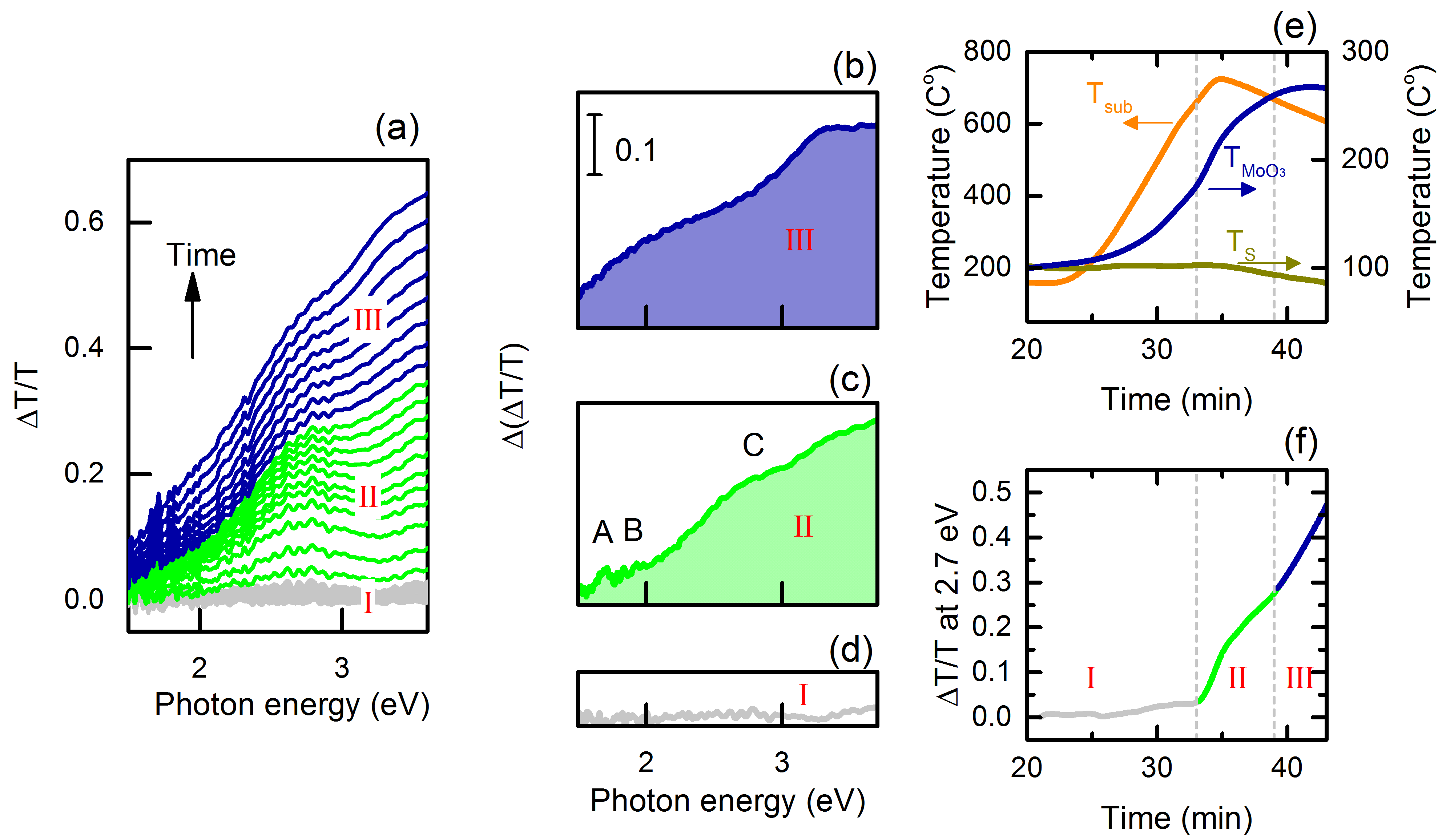
Next, let’s have a look at the evolution of the optical properties during the growth. Fig. 2(a) shows the DT spectra recorded during the CVD process. Based on the evolution of the DTS, we divide our CVD process into three sections. For the first section (section I) starting from the preheating of the sulfur source and the furnace, it can be seen that the DT spectrum remains unchanged during the first 33 min, although the temperatures measured at the positions of sulfur, MoO3 and the substrate were raised. This observation shows that no thin film was deposited during this period. The second section (section II) starting from the time min, transmittance around 2.7 eV decreases (DT signal increases) with the time. The energy position of the DTS feature at 2.7 eV coincides very nicely with the absorption peak C of the MoS2 monolayer. The continuous decrease of the optical intensity at this energy indicates the increase of the optical absorption due to the growth of the MoS2 layer on the surfaces of the sapphire substrate. In comparison with the DR spectra of the same sample measured ex-situ at room temperature (see Fig. 1(e)), the peak C is broad and shifted to the lower energy. Furthermore, the sharp absorption features A and B observed at room temperature are hardly visible. We attribute this deviation from the optical spectrum measured at room temperature to the high substrate temperature ( 700 ∘C) during growth. Indeed, the study of the temperature dependence of the absorption of MoS2 monolayer shows the same tendency [30]. Therefore, the DT spectra recorded after more than 33 min deposition show characteristic absorption of MoS2 monolayer at elevated temperature and their amplitudes increase with the deposition time. However, during the third section (section III), which starts at about 39 min, the DT signal at a higher energy of 3.2 eV became dominating. Based on its energy position, this feature can be attributed to the absorption of the MoO3 [31, 32]. As a semiconductor, MoO3 shows a bandgap around 3 eV. Considering the high temperature of the substrate, we can exclude the possibility that the MoO3 thin films were formed on the substrate surfaces. Actually, we attribute the observed DTS signal to the absorption of the MoO3 thin films which were deposited on the inner surface of the quartz window at the end of the furnace tube. Since the quartz was maintained close to room temperature, it is reasonable to assume that a small amount of the MoO3 molecules carried by the Ar flow from upstream may be deposited on the inner surface of this quartz window. The deposition rate of the MoO3 on the inner surface of the quartz window should be proportional to the product of , in which, is the concentration of MoO3 molecule above the MoO3 source which depends exponentially on the source temperature . The coefficient count on the transportation efficiency of MoO3 molecules from the source to the inner surface of the quartz window. Although the coefficient has been minimized, it was, apparently, unignorable during this study. Actually, the growth of the MoO3 feature sets in already in the second section, where the DT signal raising at 2.7 eV was accompanied by the increasing at 3.2 eV.
The characteristic increments of the DT spectrum during each section can be recognized from the spectra plotted in the central column of Fig. 2. Indeed, the increment of the DT signal over the large wavelength range is negligible during the section I (Fig. 2(d)) indicating no growth occurring on the substrate surfaces. For the section II (Fig. 2(c)), the increase of the DT signals can be clearly recognized at not only 2.7 eV but also 1.85 and 1.72 eV associating to the absorption peaks C, B and A of the growing MoS2 monolayer, respectively. In comparison with the DR spectra measured ex-situ at room temperature, a systematic red shift can be observed for all the three features verifying the influence of the substrate temperature. In addition, the absorption of the MoO3 thin films deposited on the quartz window is also clearly visible at 3.2 eV. Finally, during the section III (Fig. 2(b)), the incremental change of the DTS is dominated by the increase in the energy range above 3.2 eV. In contrast, the features associated to MoS2 becomes invisible. The decrease of the transmittance (the increase of DTS) over the low energy range could be attributed to the increase of the scattering of the MoO3 thin film deposited on the quartz window.
In order to understand the observed evolution of the DT spectroscopy, let’s have a closer inspection at its correlation with the temperature at the positions of sulfur source, MoO3 source and the substrate (see Fig. 2(e) and (f)). In Fig. 2(f), the DT signal at 2.7 eV is selected to represent the growth of the MoS2. By looking at Fig. 2(e) and (f), it becomes clear that the growth of the DT signal at 2.7 eV and thus the MoS2 layer sets in when the temperatures of the substrate and MoO3 exceed 650 ∘C and 170 ∘C, respectively. Based on the following two facts: (1) The sulfur source had been being maintained at temperatures above 100 ∘C for more than 10 min till this moment. (2) The growth of MoS2 monolayer at substrate temperature as low as 530 ∘C has been reported [11]. We thus attribute the observed onset of the MoS2 growth to the evaporation of the MoO3 reaching a recognizable rate. Afterwards, the DT signal at 2.7 eV increases monotonically revealing the ongoing growth of the MoS2 layer. Interestingly, although the temperature of the MoO3 source was still increasing, the growth speed of the DT signal at 2.7 eV dropped at around 35 min. With a closer inspection of the temperature curves, the observed decrease of the growth rate at 2.7 eV can be correlated to the declining of the substrate temperature and the sulfur source temperature. Actually, without going into the details of the kinetics of the reaction, the growth rate of the MoS2 can be associated to several factors that depend strongly on the temperatures of sulfur source (), MoO3 source () and the substrate (), respectively, in the following way:
| (1) |
where represents the effective reaction rate coefficient between MoO3 and sulfur leading to the formation of MoS2. The depends strongly on the as indicated by the Arrhenius equation. Similar to , is the concentration of the sulfur molecules over the sulfur source, which depends exponentially on . This relation emphases the strong influence of the temperature on the growth rate of MoS2. Indeed, the fast rise of the DT signal at 2.7 eV at the initial stage of the section II can be correlated nicely to the increase of the temperatures at both MoO3 source () and around the substrate (). The drop of the growth rate of the DT signal at 2.7 eV observed at 35 min coincides decently to the decrease of the temperature around the substrate () and at the source of sulfur (). The recovering of the growth rate of DT signal at 2.7 eV within the section III can not be attributed to the absorption of MoS2 anymore. Instead, it is induced by the overall decrease of transmittance through the quartz window due to the enhanced coating of the MoO3 layer. Indeed, in contrast to the decrease of and , the MoO3 source temperature keeps rising even at the beginning of the section III (see Fig. 3(e)).
3 Conclusion
In conclusion, we have grown successfully the MoS2 monolayers on both sides of the double polished c-plane sapphire substrates using CVD. The monolayers on both sides of the substrate distributed homogeneous over the substrate surfaces with a size of 10 mm 10 mm. Most importantly, the evolution of the optical transmittance of the substrate has been monitored in-situ in real time during the CVD growth using DTS. The formation of the MoS2 monolayers is clearly visible from the development of DT spectrum. More specifically, the onset of the growth and the variation of the growth rate of MoS2 monolayers can be determined. These detailed information about the growth deduced from the DTS can be correlated very nicely to the variation of the temperatures of the substrate, the MoO3 and the sulfur sources. The current result emphasizes the importance of the in-situ real time study and paves the way for deep understanding and eventually precise controlling of the growth of the 2D semiconducting materials.
4 Experimental
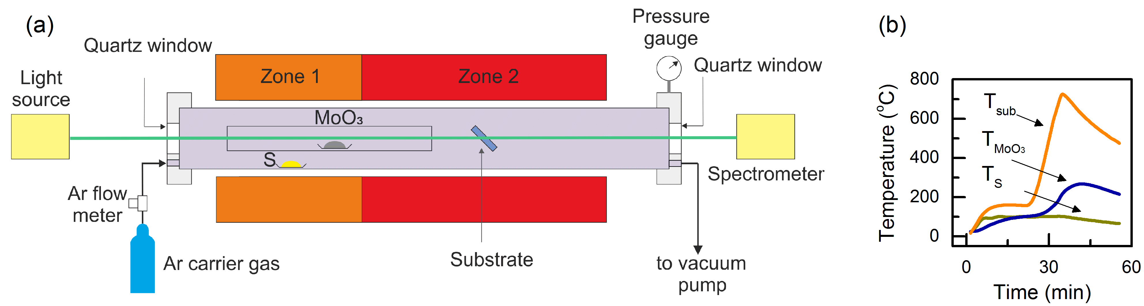
The setup of the CVD reactor including the optical spectrometer applied for the in-situ measurement is sketched in Fig. 3(a). High purity MoO3 powder is used as the precursors for molybdenum, whereas the sulfer is supplied by vaporizing solid sulfur. Ar with a high purity was used as carrier gas and a flow rate of 150 sccm was maintained during the whole process. The air in the reactor was evacuated before the inlet of the Ar gas and the pressure of Ar was maintained at 0.1 torr till the end of the process. An horizontal tube furnace with a single heating zone and a heating belt were applied as heating elements for the substrate, MoO3 and sulfur, respectively. To establish the temperature distribution required for the CVD, the substrates were positioned at the center of the furnace, while the alumina boats containing solid sulfur and MoO3 were located 15 cm and 3 cm, respectively, away from the entrance of the furnace upstream of the Ar flow. From the configuration exhibited in Fig. 3(a), it can be recognized that the sulfur is predominantly heated by the heating belt, whereas the MoO3 powder was heated not only by the heating belt but also by the heater in the furnace in a radiative manner. In order to avoid the early mixing and reaction between MoO3 and sulfur, the alumina boat of MoO3 was enclosed in a quartz tube suspended coaxially with the outer quartz tube of the CVD reactor. The distance between the exit of the inner quartz tube and the substrate was maintained as 3 cm. The evolutions of temperatures of the substrate, boats containing MoO3 and sulfur during growth are plotted in Fig.3(b). For the growth reported in this paper, double side polished c-plane sapphire (Al2O3(0001)) was selected as the substrate. During deposition, the substrates were inclined with their surface normal 45 degree off the axis of the quartz tube of the furnace (see Fig. 3(a)). At both ends of the furnace quartz tube, windows made of quartz were mounted to seal the reactor. The optical transmittance of the substrate was measured in real time using a spectroscopic ellipsometer from J.A. Woollam Co. More specifically, a beam of white light generated from a Xe lamp was guided through the substrate along the axis of the CVD reactor and detected by an spectrometer equipped with a CCD detector array. In order to enhance the sensitivity, the differential transmittance spectrum (DTS) at time was calculated using the following equation (Eq. 2):
| (2) |
where and denote the transmittance spectra of the bare substrate before the CVD process and the one after a time , respectively. The obtained DTS signal represents the change of the optical transmittance relative to the bare substrate surfaces as a function of time . Because the sapphire substrate is transparent in the wavelength range studied here, the DT spectra measured are directly associated with the absorption of the thin films deposited on the substrate. This fact makes the DTS a sensitive method for in-situ monitoring the growth of MoS2 monolayer in real time in the current study.
acknowledgements
C.B.-P and Y. W contribute equally to this work.The authors thank Assoc.Prof. Chunguang Hu and Prof. Yanning Li at Tianjin University for fruitful discussions.We acknowledge financial support for this work by the Austrian Science Fund (FWF) with project number: P25377-N20. C.B.L.P. thanks financial support from Consejo Nacional de ciencia y Tecnología, though the “Becas Mixtas” program. Y.X.W. acknowledges the financial support from Eurasia Pacific Uninet and W.F.S. acknowledges the financial support of China Scholarship Council (CSC).
References
- [1] KS Novoselov, D Jiang, F Schedin, TJ Booth, VV Khotkevich, SV Morozov, and AK Geim. Two-dimensional atomic crystals. Proceedings of the National Academy of Sciences, 102(30):10451–10453, 2005.
- [2] Kin Fai Mak, Changgu Lee, James Hone, Jie Shan, and Tony F Heinz. Atomically thin mos 2: a new direct-gap semiconductor. Physical review letters, 105(13):136805, 2010.
- [3] Qing Hua Wang, Kourosh Kalantar-Zadeh, Andras Kis, Jonathan N Coleman, and Michael S Strano. Electronics and optoelectronics of two-dimensional transition metal dichalcogenides. Nature nanotechnology, 7(11):699, 2012.
- [4] Sheneve Z. Butler, Shawna M. Hollen, Linyou Cao, Yi Cui, Jay A. Gupta, Humberto R. Gutiérrez, Tony F. Heinz, Seung Sae Hong, Jiaxing Huang, Ariel F. Ismach, Ezekiel Johnston-Halperin, Masaru Kuno, Vladimir V. Plashnitsa, Richard D. Robinson, Rodney S. Ruoff, Sayeef Salahuddin, Jie Shan, Li Shi, Michael G. Spencer, Mauricio Terrones, Wolfgang Windl, and Joshua E. Goldberger. Progress, challenges, and opportunities in two-dimensional materials beyond graphene. ACS nano, 7(4):2898–2926, 2013.
- [5] Xiaodong Xu, Wang Yao, Di Xiao, and Tony F Heinz. Spin and pseudospins in layered transition metal dichalcogenides. Nature Physics, 10(5):343, 2014.
- [6] Sajedeh Manzeli, Dmitry Ovchinnikov, Diego Pasquier, Oleg V Yazyev, and Andras Kis. 2d transition metal dichalcogenides. Nature Reviews Materials, 2(8):17033, 2017.
- [7] Zhong Lin, Amber McCreary, Natalie Briggs, Shruti Subramanian, Kehao Zhang, Yifan Sun, Xufan Li, Nicholas J Borys, Hongtao Yuan, Susan K Fullerton-Shirey, Alexey Chernikov, Hui Zhao, Stephen McDonnell, Aaron M Lindenberg, Kai Xiao, Brian J LeRoy, Marija Drndić, James C M Hwang, Jiwoong Park, Manish Chhowalla, Raymond E Schaak, Ali Javey, Mark C Hersam, Joshua Robinson, and Mauricio Terrones. 2d materials advances: from large scale synthesis and controlled heterostructures to improved characterization techniques, defects and applications. 2D Materials, 3(4):042001, 2016.
- [8] Yi-Hsien Lee, Xin-Quan Zhang, Wenjing Zhang, Mu-Tung Chang, Cheng-Te Lin, Kai-Di Chang, Ya-Chu Yu, Jacob Tse-Wei Wang, Chia-Seng Chang, Lain-Jong Li, and Tsung-Wu Lin. Synthesis of large-area mos2 atomic layers with chemical vapor deposition. Advanced materials, 24(17):2320–2325, 2012.
- [9] Yi-Hsien Lee, Lili Yu, Han Wang, Wenjing Fang, Xi Ling, Yumeng Shi, Cheng-Te Lin, Jing-Kai Huang, Mu-Tung Chang, Chia-Seng Chang, Mildred Dresselhaus, Tomas Palacios, Lain-Jong Li, and Jing Kong. Synthesis and transfer of single-layer transition metal disulfides on diverse surfaces. Nano letters, 13(4):1852–1857, 2013.
- [10] Shanshan Wang, Youmin Rong, Ye Fan, Mercè Pacios, Harish Bhaskaran, Kuang He, and Jamie H. Warner. Shape evolution of monolayer mos2 crystals grown by chemical vapor deposition. Chemistry of Materials, 26(22):6371–6379, 2014.
- [11] Qingqing Ji, Min Kan, Yu Zhang, Yao Guo, Donglin Ma, Jianping Shi, Qiang Sun, Qing Chen, Yanfeng Zhang, and Zhongfan Liu. Unravelling orientation distribution and merging behavior of monolayer mos2 domains on sapphire. Nano letters, 15(1):198–205, 2014.
- [12] Dumitru Dumcenco, Dmitry Ovchinnikov, Kolyo Marinov, Predrag Lazić, Marco Gibertini, Nicola Marzari, Oriol Lopez Sanchez, Yen-Cheng Kung, Daria Krasnozhon, Ming-Wei Chen, Simone Bertolazzi, Philippe Gillet, Anna Fontcuberta i Morral, Aleksandra Radenovic, and Andras Kis. Large-area epitaxial monolayer mos2. ACS nano, 9(4):4611–4620, 2015.
- [13] Kibum Kang, Saien Xie, Lujie Huang, Yimo Han, Pinshane Y Huang, Kin Fai Mak, Cheol-Joo Kim, David Muller, and Jiwoong Park. High-mobility three-atom-thick semiconducting films with wafer-scale homogeneity. Nature, 520(7549):656, 2015.
- [14] Hua Yu, Mengzhou Liao, Wenjuan Zhao, Guodong Liu, X. J. Zhou, Zheng Wei, Xiaozhi Xu, Kaihui Liu, Zonghai Hu, Ke Deng, Shuyun Zhou, Jin-An Shi, Lin Gu, Cheng Shen, Tingting Zhang, Luojun Du, Li Xie, Jianqi Zhu, Wei Chen, Rong Yang, Dongxia Shi, and Guangyu Zhang. Wafer-scale growth and transfer of highly-oriented monolayer mos2 continuous films. ACS nano, 11(12):12001–12007, 2017.
- [15] Jingxin Cheng, Tao Jiang, Qingqing Ji, Yu Zhang, Zhiming Li, Yuwei Shan, Yanfeng Zhang, Xingao Gong, Weitao Liu, and Shiwei Wu. Kinetic nature of grain boundary formation in as-grown mos2 monolayers. Advanced Materials, 27(27):4069–4074, 2015.
- [16] Wei Chen, Jing Zhao, Jing Zhang, Lin Gu, Zhenzhong Yang, Xiaomin Li, Hua Yu, Xuetao Zhu, Rong Yang, Dongxia Shi, Xuechun Lin, Jiandong Guo, Xuedong Bai, and Guangyu Zhang. Oxygen-assisted chemical vapor deposition growth of large single-crystal and high-quality monolayer mos2. Journal of the American Chemical Society, 137(50):15632–15635, 2015.
- [17] Jeffrey D Cain, Fengyuan Shi, Jinsong Wu, and Vinayak P Dravid. Growth mechanism of transition metal dichalcogenide monolayers: the role of self-seeding fullerene nuclei. ACS nano, 10(5):5440–5445, 2016.
- [18] Ananth Govind Rajan, Jamie H Warner, Daniel Blankschtein, and Michael S Strano. Generalized mechanistic model for the chemical vapor deposition of 2d transition metal dichalcogenide monolayers. ACS nano, 10(4):4330–4344, 2016.
- [19] HoKwon Kim, Dmitry Ovchinnikov, Davide Deiana, Dmitrii Unuchek, and Andras Kis. Suppressing nucleation in metal–organic chemical vapor deposition of mos2 monolayers by alkali metal halides. Nano letters, 17(8):5056–5063, 2017.
- [20] Yilei Li, Alexey Chernikov, Xian Zhang, Albert Rigosi, Heather M Hill, Arend M van der Zande, Daniel A Chenet, En-Min Shih, James Hone, and Tony F Heinz. Measurement of the optical dielectric function of monolayer transition-metal dichalcogenides: Mos 2, mo s e 2, ws 2, and ws e 2. Physical Review B, 90(20):205422, 2014.
- [21] Debdeep Jena and Aniruddha Konar. Enhancement of carrier mobility in semiconductor nanostructures by dielectric engineering. Physical review letters, 98(13):136805, 2007.
- [22] Shinichiro Mouri, Yuhei Miyauchi, and Kazunari Matsuda. Tunable photoluminescence of monolayer mos2 via chemical doping. Nano letters, 13(12):5944–5948, 2013.
- [23] Sefaattin Tongay, Jian Zhou, Can Ataca, Jonathan Liu, Jeong Seuk Kang, Tyler S Matthews, Long You, Jingbo Li, Jeffrey C Grossman, and Junqiao Wu. Broad-range modulation of light emission in two-dimensional semiconductors by molecular physisorption gating. Nano letters, 13(6):2831–2836, 2013.
- [24] Hiram J Conley, Bin Wang, Jed I Ziegler, Richard F Haglund Jr, Sokrates T Pantelides, and Kirill I Bolotin. Bandgap engineering of strained monolayer and bilayer mos2. Nano letters, 13(8):3626–3630, 2013.
- [25] Roman Forker and Torsten Fritz. Optical differential reflectance spectroscopy of ultrathin epitaxial organic films. Physical Chemistry Chemical Physics, 11(13):2142–2155, 2009.
- [26] Gianlorenzo Bussetti, Marcello Campione, Michele Riva, Andrea Picone, Luisa Raimondo, Lorenzo Ferraro, Conor Hogan, Maurizia Palummo, Alberto Brambilla, Marco Finazzi, Lamberto Duò, Adele Sassella, and Franco Ciccacci. Stable alignment of tautomers at room temperature in porphyrin 2d layers. Advanced Functional Materials, 24(7):958–963, 2014.
- [27] Yaxu Wei, Wanfu Shen, Dietmar Roth, Sen Wu, Chunguang Hu, Yanning Li, Xiaotang Hu, Michael Hohage, Peter Bauer, and Lidong Sun. Real-time monitoring of 2d semiconductor film growth with optical spectroscopy. Nanotechnology, 28(46):465601, 2017.
- [28] Philipp Tonndorf, Robert Schmidt, Philipp Böttger, Xiao Zhang, Janna Börner, Andreas Liebig, Manfred Albrecht, Christian Kloc, Ovidiu Gordan, Dietrich R. T. Zahn, Steffen Michaelis de Vasconcellos, and Rudolf Bratschitsch. Photoluminescence emission and raman response of monolayer mos 2, mose 2, and wse 2. Optics express, 21(4):4908–4916, 2013.
- [29] Diana Y Qiu, H Felipe, and Steven G Louie. Optical spectrum of mos 2: many-body effects and diversity of exciton states. Physical review letters, 111(21):216805, 2013.
- [30] Eilam Yalon, Özgür Burak Aslan, Kirby K. H. Smithe, Connor J. McClellan, Saurabh V. Suryavanshi, Feng Xiong, Aditya Sood, Christopher M. Neumann, Xiaoqing Xu, Kenneth E. Goodson, Tony F. Heinz, and Eric Pop. Temperature-dependent thermal boundary conductance of monolayer mos2 by raman thermometry. ACS applied materials & interfaces, 9(49):43013–43020, 2017.
- [31] Minoru Itoh, Kousuke Hayakawa, and Shuji Oishi. Optical properties and electronic structures of layered moo3 single crystals. Journal of Physics: Condensed Matter, 13(31):6853, 2001.
- [32] Isabela Alves de Castro, Robi Shankar Datta, Jian Zhen Ou, Andres Castellanos-Gomez, Sharath Sriram, Torben Daeneke, and Kourosh Kalantar-zadeh. Molybdenum oxides–from fundamentals to functionality. Advanced Materials, 29(40):1701619, 2017.