Consistency between ARPES and STM measurements on SmB6
Abstract
The Kondo insulator SmB6 has emerged as a primary candidate for exotic quantum phases, due to the predicted formation of strongly-correlated, low-velocity topological surface states, and corresponding high Fermi-level density of states. However, measurements of the surface-state velocity in SmB6 differ by orders of magnitude, depending on the experimental technique used. Here we reconcile two techniques, scanning tunneling microscopy (STM) and angle-resolved photoemission spectroscopy (ARPES), by accounting for surface band bending on polar terminations. Using spatially-resolved scanning tunneling spectroscopy (STS), we measure a band shift of meV between full-Sm and half-Sm terminations, in qualitative agreement with our density functional theory (DFT) calculations of the surface charge density. Furthermore, we reproduce the apparent high-velocity surface states reported by ARPES, by simulating their observed spectral function as an equal-weight average over the two band-shifted domains that we image by STM. Our results highlight the necessity of local measurements to address inhomogeneously-terminated surfaces, or fabrication techniques to achieve uniform termination for meaningful large-area surface measurements of polar crystals such as SmB6.
I Introduction
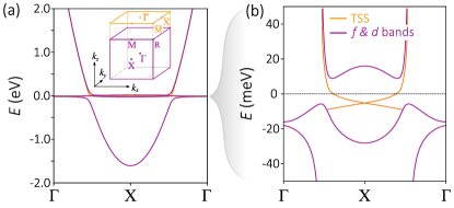
In a Kondo insulator (KI), strong interactions between localized electrons renormalize their spectral weight towards the chemical potential. Below a characteristic temperature , conduction electrons begin to scatter from these renormalized states, opening a hybridization gap at the Fermi level. In a subset of KIs called topological Kondo insulators, this gap can encode a non-trivial bulk topological invariant, leading to the appearance of protected surface states Dzero et al. (2016); Misra (2008). In the KI SmB6, the onset of the hybridization gap leads to a resistivity upturn below K Kim et al. (2014); Allen et al. (1979); Cooley et al. (1995). Yet, rather than diverging, the resistivity saturates below 5 K, indicating the emergence of an additional conduction channel Wolgast et al. (2013); Syers et al. (2015). This conduction channel has been attributed to topological surface states by several theoretical studies, which span complementary approaches including renormalized band theory and tight-binding Hamiltonians matched to LDA (+Gutzwiller) calculations Dzero et al. (2010); Lu et al. (2013); Alexandrov et al. (2013). These calculations predict the existence of three surface Dirac cones with heavy quasiparticles, of predominantly character, as shown schematically in Fig. 1. Such low-velocity Dirac fermions would provide a high density of states at the Fermi level, increasing their susceptibility to exotic orders and their potential utility Alexandrov et al. (2013); Chen et al. (2014); Efimkin and Galitski (2014); Thomson and Sachdev (2016). However, the empirical identification of the additional conduction channel Wolgast et al. (2013); Syers et al. (2015) with the predicted topological surface states Dzero et al. (2010); Lu et al. (2013); Alexandrov et al. (2013) has remained controversial due to apparent contradictions between different experimental techniques.
Experimentally, angle-resolved photoemission spectroscopy (ARPES) and scanning tunneling microscopy (STM) have each identified key features of the topological states in SmB6, but with quantitative and qualitative differences. At low temperatures, ARPES studies reported a hybridization gap that hosts linearly dispersing surface states Denlinger et al. (2014); Xu et al. (2013, 2014a); Neupane et al. (2013); Jiang et al. (2013) with a non-trivial spin texture Xu et al. (2014b); Suga et al. (2013).
| Theory Lu et al. (2013) | STM Pirie et al. (2020) | ARPES Jiang et al. (2013) | Quantum Oscillation Li et al. (2014) | |
|---|---|---|---|---|
| (meVÅ) | ||||
| (meV) | ||||
| () | ||||
| (meVÅ) | ||||
| (meV) | ||||
However, the apparent velocity of these states is an order of magnitude higher than theoretically predicted (see Table 1). Meanwhile, the hallmark of a topological surface state—its Dirac point—has not been clearly resolved in any ARPES experiment to date Xu et al. (2014a), leading to the suggestion that it has been pushed into the valence band by a strong surface potential Roy et al. (2014), or by the breakdown of the Kondo effect at the surface Alexandrov et al. (2015). On the other hand, milliKelvin scanning tunneling spectroscopy (STS) studies identified several strong resonances within the hybridization gap, consistent with low-velocity surface states Jiao et al. (2016); Sun et al. (2018). Additionally, momentum-resolved STM directly imaged linearly dispersing low-velocity surface states that converge to a Dirac point within the gap Pirie et al. (2020), consistent with theoretical predictions Lu et al. (2013).
The apparent inconsistencies between STM and ARPES arise from the different experimental length scales for each technique. STM typically images hundred-nanometer regions with picometer spatial resolution. On SmB6, STM universally observes surface domains with sizes on the order of tens of nanometers Ruan et al. (2014); Rößler et al. (2014); Jiao et al. (2016); Sun et al. (2018); Pirie et al. (2020); Yee et al. (2013), consistent with its polar structure and the lack of a natural cleavage plane. Yet the typical ARPES spot size is on the order of tens of microns Xu et al. (2016), and consequently averages over thousands of SmB6 surface domains. This averaging poses a problem if the various domains exhibit polarity-driven band bending, as ARPES spectra will contain a superposition of spectral features, shifted in energy with respect to one another.
Here we use STM spectroscopy to guide a simulation of the spectral functions on polar Sm and non-polar Sm terminations, using the energy and momentum broadening of typical ARPES experiments. For a range of realistic experimental parameters, our simulated ARPES spectra show topological surface states with an artificially enhanced Fermi velocity and a buried Dirac point, similar to published experimental ARPES results. Our findings provide the long-sought, fully-consistent explanation for the apparent discrepancy between the band structure measured by ARPES and STM. They further confirm the consistency between STM and theoretical predictions of low-velocity surface states with an in-gap Dirac point and high density of states at the Fermi level.
II Methods
II.1 Scanning tunneling microscopy/spectroscopy
We performed STM experiments on single crystals of SmB6 grown using the Al-flux method Nakajima et al. (2016); Kim et al. (2013). We cleaved the crystals in cryogenic ultra-high vacuum at K before inserting them into the STM head. We prepared PtIr STM tips by ex situ mechanical sharpening then in situ field emission on Au foil.
II.2 Calculations
We performed calculations in the framework of density functional theory (DFT), as implemented in the Quantum ESPRESSO package Giannozzi et al. (2009). We calculated the exchange-correlation functional using the generalized gradient approximation of Perdew-Burke-Ernzerhof (GGA-PBE) Perdew et al. (1996). The electron-ion interactions are described by ultrasoft pseudopotentials with valence electron configurations of for B atoms and for Sm atoms. The energy cutoff for the plane wave basis is 120 Ry with a charge density cutoff of 500 Ry. We used a Monkhorst-Pack Monkhorst and Pack (1976) scheme with a k-mesh for the Brillouin zone integration for the supercell with one unit cell ( Sm) and -mesh for the supercell with two unit cells ( Sm). In all calculations, the lattice parameter was fixed at the experimental value Å, with slab thickness Å and vacuum thickness 15 Å to minimize interactions between the periodic images. We did not consider spin polarization or spin-orbit coupling since our focus is on the electrostatics of the material.
III Results
III.1 Surface characterization
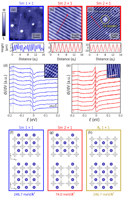
Due to its lack of a natural cleavage plane, an abundance of distinct surface terminations have been observed by STM on SmB6 Rößler et al. (2016). Across a dozen STM experiments, the largest reported domain of an ordered surface on pristine SmB6 ( dopants) is only 60 nm Yee et al. (2013); Ruan et al. (2014); Rößler et al. (2014); Jiao et al. (2016); Sun et al. (2018); Pirie et al. (2020); Rößler et al. (2016); Jiao et al. (2018); Herrmann et al. . Two commonly observed surfaces are the square lattice [Fig. 2(a)] and the rows that arise when half of the Sm atoms are removed during cleaving [Fig. 2(b) and 2(c)] Rößler et al. (2016); data underlying Figs. 1 5 can be accessed at . The surface has also been observed by low-energy electron diffraction Ramankutty et al. (2016) and ARPES, where it manifests as Umklapp scattering Hlawenka et al. (2018); Xu et al. (2013). We confirmed the identity of the surface using lightly Fe-doped samples where Fe is known to substitute for Sm Akintola et al. (2017); we observed individual Fe-atom signatures centered on the rows of Sm atoms in Fig. 2(c). We confirmed the identity of the lattice presented in Fig. 2(a) as a full Sm layer due to the direction of its band bending compared to the surface, as shown in Fig. 2(d-e) and discussed in more detail below.
The relative prevalence of each surface can be understood from its formation energy [Figs. 2(f-h)]. Although most STM reports have focused on the surface Jiao et al. (2016); Rößler et al. (2014); Sun et al. (2018); Ruan et al. (2014), our more frequent observation of the surface is consistent with its lower formation energy as calculated by DFT. In general, a more balanced charge distribution on either side of the cleave, as drawn in Fig. 2(g), is intuitively expected to lower the surface formation energy.
III.2 Termination-dependent band bending
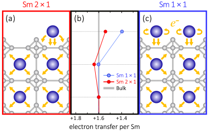
In general, the surface termination can cause a redistribution of charge that affects the local electronic structure, an effect well studied in conventional semiconductors Zhang and Yates (2012). In bulk SmB6, Sm atoms donate equal amounts of charge to the B6 octahedra above and below them. However, on the surface the Sm atoms are under-coordinated; the B layer beneath the topmost Sm layer cannot accept all of the excess electrons, so they accumulate on the surface. This charge accumulation is qualitatively captured in our calculations of the electron transfer, which use Bader analysis to partition the DFT charge density (Fig. 3).
The increased electron density near the surface leads to reduced surface charge transfer shown as a blue line in Fig. 3(b), greater filling of the Sm orbitals, and to a slight downward bending of the surface bands. On the other hand, Sm atoms at the surface can donate a greater fraction of their electrons to the B layer below, because there are only half as many Sm atoms at the surface as in the bulk. Correspondingly, we found only a minor deviation in the calculated charge transfer at the surface, shown as a red line in Fig. 3(b). Although our Bader charge analysis quantitatively departs from the experimental Sm valence of around Tarascon et al. (1980), it provides a qualitative understanding of the charge transfer on the SmB6 surface.
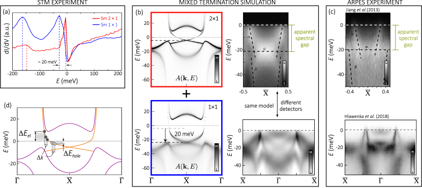
To experimentally determine the accumulation of surface charge, we measured local differential conductance, , where is the tunneling current and is the bias applied to the sample with respect to the tip. On a typical ordered domain, there are three pronounced spectral features: a peak around meV, a peak just below , and a shoulder around meV, as shown in Fig. 4(a). The two filled-state peaks predominantly reflect contributions from the Sm states, as determined by previous STM and ARPES measurements, and by dynamical mean-field theory calculations Yee et al. (2013); Pirie et al. (2020); Sun et al. (2018); Denlinger et al. . Although the peak energies are homogeneous within each ordered domain [see Fig. 2(d-e)], we found that the peaks are shifted downward on the surface by about 20 meV compared to the surface.
III.3 Spectral function simulation
ARPES spectra can be broadened by local band bending if the spot size encompasses multiple surface domains of different polarity. We investigated this possibility in SmB6 by deriving a spectral function for each termination, from our STM measurements Pirie et al. (2020). In accordance with our data, our simulation includes low-velocity Dirac states close to the chemical potential, connecting a light bulk band to two heavy bulk bands. Each state includes a Fermi-liquid-like quasiparticle decay rate Varma et al. (2002). We simulated each termination by adjusting the energies of the and bands to match our STM spectra. Specifically, in the spectral-function simulation, the occupied states are shifted down by 20 meV relative to the simulation. We simulated ARPES spectra by computing an equal-weighted average of the spectral functions for each surface, then convolving the result with a Gaussian kernel that accounts for detector resolution and temperature broadening as shown in right panels of Fig. 4(b). Specifically, we mimic the detectors in Ref. Jiang et al. (2013) with parameters K, meV, and , and Ref. Hlawenka et al. (2018) with parameters K, meV, and . In each case, our simulation captures the main features of the measured ARPES spectra as reproduced in Fig. 4(c): an apparent hybridization gap of approximately 20 meV, and in-gap surface states with an apparent high velocity, which seem to extrapolate to a buried Dirac point 111The crystal-field-split state is missing in our STM-derived simulation, but present in ARPES experiments. The discrepancy arises because STM does not couple strongly to the state, which lacks the correct symmetry to hybridize. However the lack of hybridization also means that the state does not play an important role in Kondo or topological physics..
IV Discussion
A complete understanding of the cleaved SmB6 surface requires considering both electron-rich surfaces, such as the Sm surface, and electron-deficient surfaces, such as the B-rich terminations. Importantly, our STM measurements have shown that the heavy Dirac surface states become flat only below the chemical potential Pirie et al. (2020), leading to a highly electron-hole-asymmetric band-bending scenario, as depicted in Fig. 4(d) and Fig. 5. In such a scenario, we expect that surplus electrons, as found on Sm terminations, primarily populate the steeper (upper) part of the surface-state dispersion [see Fig. 1(b)], producing a notable downward shift of spectral features, as shown in Fig. 4(a). Conversely, a surface deficient of electrons, as expected for B-rich terminations, would depopulate the very flat (lower) part of the surface-state dispersion. Due to the dramatic difference in band slope (velocity) above and below the Fermi level, spectral features would be shifted upward by much less on a surface with missing electrons, than they would be shifted downward on a surface with the same number of excess electrons. Indeed, on B6 surfaces, STM measured a prominent peak at meV Jiao et al. (2016), which is shifted upward by only 1.5 meV compared to the corresponding peak on the neutral Sm surface [see Fig. 4(a)]. Thus, the total band-bending range, defined by the most negatively charged Sm termination and the most positively charged B6 termination, is 21.5 meV, as shown in Fig. 5. Therefore, our ARPES simulation, using data from the two surfaces we observe, covers more than 90% of the maximum possible surface band-bending.
While our study focuses on the (001) surface, recent ARPES experiments also reported high-velocity surface states on the (110) and (111) surfaces Ohtsubo et al. (2019); Denlinger et al. . These reports are surprising because both surfaces are nominally non-polar and hence are expected to host low-velocity Dirac states. In fact, magnetothermoelectric studies have already indicated the presence of heavy metallic states on the (110) surface Luo et al. (2015), contrary to the ARPES measurement. Under closer inspection by STM, the (110) surface appears to be inhomogeneous on small length scales Rößler et al. (2016). The intense atomic-scale disorder may alter the local electronic environment and cause local charging, analogous to termination-dependent band bending on the (100) surface Sun et al. (2018). This local charging would be averaged in ARPES measurements, possibly resulting in enhanced surface-state velocities, similar to our simulations on the (100) surface (Fig. 4).
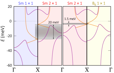
Band bending on SmB6 may also affect the perception of the hybridization gap and explain the apparent discrepancy between its size, as reported by ARPES and STM. ARPES generally reports 15-20 meV for the part of the hybridization gap below , as shown in Fig. 4(c) Denlinger et al. (2014); Xu et al. (2013, 2014a); Neupane et al. (2013); Jiao et al. (2016); Hlawenka et al. (2018), while the full gap, as measured by STM, is only 8-15 meV Pirie et al. (2020); Ruan et al. (2014); Sun et al. (2018); Jiao et al. (2016). In Fig. 4(b), our ARPES simulation shows a large gap below , of about 25 meV, despite arising from a band structure with a gap of only 15 meV on the non-polar surface, as measured by STM. Specifically, averaging over different surface terminations blurs the top of the bulk valence band, which introduces an apparent increase of the hybridization gap on the occupied side. The full impact of excess charge on the surface Kondo environment and d-f hybridization remains an open theoretical question Alexandrov et al. (2015).
V Conclusion
SmB6 is a promising platform for devices that exploit correlated topological phases, but its cubic and polar structure give rise to small, charged surface domains, on which band bending may locally distort the Dirac surface states. Using STM spectroscopy, we investigated two distinct surface terminations and measured a band shift of about 20 meV between them. These measurements guided a simulation of ARPES spectra, which captures the essential experimental features of ARPES, but remains consistent with STM conclusions Pirie et al. (2020). Our results suggest that band bending is most pronounced on Sm-rich terminations, motivating the development of new surface treatments or epitaxial-growth techniques such as molecular beam epitaxy to achieve a more uniform termination. Control over the termination would allow the important correlated surface states to be tuned closer to the Fermi level, without introducing disorder through chemical doping, which would be advantageous for future applications Yong et al. (2014).
Acknowledgements
We thank Jonathan Denlinger, Emile Rienks and Yun Suk Eo for enlightening discussions and Johnpierre Paglione, Xiangfeng Wang, Zachary Fisk and Dae-Jeong Kim for providing the samples. Experiments were supported by National Science Foundation DMR-1410480 and partially as part of the Center for the Advancement of Topological Semimetals, an Energy Frontier Research Center funded by the U.S. Department of Energy (DOE), Office of Science, Basic Energy Sciences (BES) through the Ames Laboratory under its Contract No. DE-AC02-07CH11358 (STM measurements). HP and MHH were funded by the Gordon and Betty Moore Foundation’s EPiQS Initiative through Grant GBMF4536. CEM is supported by the Swiss National Science Foundation under fellowships P2EZP2_175155 and P400P2_183890. JJP and WP acknowledge Sahar Pakdel for her contribution at the initial stages of the theoretical work and financial support from Spanish MINECO through Grant FIS2016-80434-P, the Fundación Ramón Areces, the María de Maeztu Program for Units of Excellence in R&D (MDM-2014-0377), the Comunidad Autónoma de Madrid through the Nanomag COST-CM Program (S2018/NMT-4321), and the European Union Seventh Framework Programme under Grant agreement No. 604391 Graphene Flagship. WP was funded by the CNPq Fellowship programme (Pós-doutorado júnior) under grant 405107/2017-0 and acknowledges the computer resources and assistance provided by the Centro de Computación Científica of the Universidad Autónoma de Madrid and the computer resources at MareNostrum and the technical support provided by Barcelona Supercomputing Center (FI-2019-2-0007).
References
- Dzero et al. (2016) Maxim Dzero, Jing Xia, Victor Galitski, and Piers Coleman, “Topological Kondo insulators,” Annual Review of Condensed Matter Physics 7, 249–280 (2016).
- Misra (2008) Prasanta Misra, in Handbook of Metal Physics, Heavy-Fermion Systems, Chapter 11 Kondo Insulators, Vol. 2, edited by Prasanta Misra (Elsevier, 2008) pp. 291–333.
- Kim et al. (2014) D. J. Kim, J. Xia, and Z. Fisk, “Topological surface state in the Kondo insulator samarium hexaboride,” Nature Materials 13, 466–470 (2014).
- Allen et al. (1979) J. W. Allen, B. Batlogg, and P. Wachter, “Large low-temperature Hall effect and resistivity in mixed-valent SmB6,” Physical Review B 20, 4807–4813 (1979).
- Cooley et al. (1995) J. C. Cooley, M. C. Aronson, Z. Fisk, and P. C. Canfield, “SmB6: Kondo insulator or exotic metal?” Phys. Rev. Lett. 74, 1629–1632 (1995).
- Wolgast et al. (2013) Steven Wolgast, Çağlıyan Kurdak, Kai Sun, J. W. Allen, Dae-Jeong Kim, and Zachary Fisk, “Low-temperature surface conduction in the Kondo insulator SmB6,” Physical Review B 88, 180405 (2013).
- Syers et al. (2015) Paul Syers, Dohun Kim, Michael S. Fuhrer, and Johnpierre Paglione, “Tuning bulk and surface conduction in the proposed topological kondo insulator SmB6,” Physical Review Letters 114, 096601 (2015).
- Dzero et al. (2010) Maxim Dzero, Kai Sun, Victor Galitski, and Piers Coleman, “Topological Kondo insulators,” Physical Review Letters 104, 106408 (2010).
- Lu et al. (2013) Feng Lu, JianZhou Zhao, Hongming Weng, Zhong Fang, and Xi Dai, “Correlated topological insulators with mixed valence,” Physical Review Letters 110, 096401 (2013).
- Alexandrov et al. (2013) Victor Alexandrov, Maxim Dzero, and Piers Coleman, “Cubic topological Kondo insulators,” Physical Review Letters 111, 226403 (2013).
- Chen et al. (2014) Xie Chen, Lukasz Fidkowski, and Ashvin Vishwanath, “Symmetry Enforced Non-Abelian Topological Order at the Surface of a Topological Insulator,” Physical Review B 89, 165132 (2014).
- Efimkin and Galitski (2014) Dmitry K. Efimkin and Victor Galitski, “Strongly interacting Dirac liquid on the surface of a topological Kondo insulator,” Physical Review B 90, 081113(R) (2014).
- Thomson and Sachdev (2016) Alex Thomson and Subir Sachdev, “Fractionalized Fermi liquid on the surface of a topological Kondo insulator,” Physical Review B 93, 125103 (2016).
- Denlinger et al. (2014) Jonathan D. Denlinger, James W. Allen, Jeong-Soo Kang, Kai Sun, Byung-II Min, Dae-Jeong Kim, and Zachary Fisk, “SmB6 photoemission: Past and present,” in Proceedings of the International Conference on Strongly Correlated Electron Systems (SCES2013) (JPS Conf. Proc. 3, 017038, 2014).
- Xu et al. (2013) N. Xu, X. Shi, P. K. Biswas, C. E. Matt, R. S. Dhaka, Y. Huang, N. C. Plumb, M. Radović, J. H. Dil, E. Pomjakushina, K. Conder, A. Amato, Z. Salman, D. McK. Paul, J. Mesot, H. Ding, and M. Shi, “Surface and bulk electronic structure of the strongly correlated system SmB6 and implications for a topological Kondo insulator,” Physical Review B 88, 121102(R) (2013).
- Xu et al. (2014a) N. Xu, C. E. Matt, E. Pomjakushina, X. Shi, R. S. Dhaka, N. C. Plumb, M. Radović, P. K. Biswas, D. Evtushinsky, V. Zabolotnyy, J. H. Dil, K. Conder, J. Mesot, H. Ding, and M. Shi, “Exotic Kondo crossover in a wide temperature region in the topological Kondo insulator SmB6 revealed by high-resolution ARPES,” Physical Review B 90, 085148 (2014a).
- Neupane et al. (2013) M. Neupane, N. Alidoust, S.-Y. Xu, T. Kondo, Y. Ishida, D. J. Kim, Chang Liu, I. Belopolski, Y. J. Jo, T.-R. Chang, H.-T. Jeng, T. Durakiewicz, L. Balicas, H. Lin, A. Bansil, S. Shin, Z. Fisk, and M. Z. Hasan, “Surface electronic structure of the topological Kondo-insulator candidate correlated electron system SmB6,” Nature Communications 4, 2991 (2013).
- Jiang et al. (2013) J. Jiang, S. Li, T. Zhang, Z. Sun, F. Chen, Z. R. Ye, M. Xu, Q. Q. Ge, S. Y. Tan, X. H. Niu, M. Xia, B. P. Xie, Y. F. Li, X. H. Chen, H. H. Wen, and D. L. Feng, “Observation of possible topological in-gap surface states in the Kondo insulator SmB6 by photoemission,” Nature Communications 4, 3010 (2013).
- Xu et al. (2014b) N. Xu, P. K. Biswas, J. H. Dil, R. S. Dhaka, G. Landolt, S. Muff, C. E. Matt, X. Shi, N. C. Plumb, M. Radović, E. Pomjakushina, K. Conder, A. Amato, S. V. Borisenko, R. Yu, H.-M. Weng, Z. Fang, X. Dai, J. Mesot, H. Ding, and M. Shi, “Direct observation of the spin texture in SmB6 as evidence of the topological Kondo insulator,” Nature Communications 5, 4566 (2014b).
- Suga et al. (2013) Shigemasa Suga, Kazuyuki Sakamoto, Taichi Okuda, Koji Miyamoto, Kenta Kuroda, Akira Sekiyama, Junichi Yamaguchi, Hidenori Fujiwara, Akinori Irizawa, Takahiro Ito, Shinichi Kimura, T. Balashov, W. Wulfhekel, S. Yeo, Fumitoshi Iga, and Shin Imada, “Spin-polarized angle-resolved photoelectron spectroscopy of the so-predicted Kondo topological insulator SmB6,” Journal of the Physical Society of Japan 83, 014705 (2013).
- Pirie et al. (2020) Harris Pirie, Yu Liu, Anjan Soumyanarayanan, Pengcheng Chen, Yang He, M. M. Yee, P. F. S. Rosa, J. D. Thompson, Dae-Jeong Kim, Z. Fisk, Xiangfeng Wang, Johnpierre Paglione, Dirk K. Morr, M. H. Hamidian, and Jennifer E. Hoffman, “Imaging emergent heavy Dirac fermions of a topological Kondo insulator,” Nature Physics 16, 52–56 (2020).
- Li et al. (2014) G. Li, Z. Xiang, F. Yu, T. Asaba, B. Lawson, P. Cai, C. Tinsman, A. Berkley, S. Wolgast, Y. S. Eo, Dae-Jeong Kim, C. Kurdak, J. W. Allen, K. Sun, X. H. Chen, Y. Y. Wang, Z. Fisk, and Lu Li, “Two-dimensional Fermi surfaces in Kondo insulator SmB6,” Science 346, 1208–1212 (2014).
- Roy et al. (2014) Bitan Roy, Jay D Sau, Maxim Dzero, and Victor Galitski, “Surface theory of a family of topological Kondo insulators,” Physical Review B 90, 155314 (2014).
- Alexandrov et al. (2015) Victor Alexandrov, Piers Coleman, and Onur Erten, “Kondo breakdown in topological Kondo insulators,” Physical Review Letters 114, 177202 (2015).
- Jiao et al. (2016) L. Jiao, S. Rößler, D. J. Kim, L. H. Tjeng, Z. Fisk, F. Steglich, and S. Wirth, “Additional energy scale in SmB6 at low-temperature,” Nature Communications 7, 13762 (2016).
- Sun et al. (2018) Zhixiang Sun, Ana Maldonado, Wendel S. Paz, Dmytro S. Inosov, Andreas P. Schnyder, J. J. Palacios, Natalya Yu. Shitsevalova, Vladimir B. Filipov, and Peter Wahl, “Observation of a well-defined hybridization gap and in-gap states on the SmB6(001) surface,” Physical Review B 97, 235107 (2018).
- Ruan et al. (2014) Wei Ruan, Cun Ye, Minghua Guo, Fei Chen, Xianhui Chen, Guang-Ming Zhang, and Yayu Wang, “Emergence of a coherent in-gap state in the Kondo insulator revealed by scanning tunneling spectroscopy,” Physical Review Letters 112, 136401 (2014).
- Rößler et al. (2014) Sahana Rößler, Tae-Hwan Jang, Dae-Jeong Kim, L. H. Tjeng, Zachary Fisk, Frank Steglich, and Steffen Wirth, “Hybridization gap and Fano resonance in SmB6,” Proceedings of the National Academy of Sciences 111, 4798–4802 (2014).
- Yee et al. (2013) Michael M. Yee, Yang He, Anjan Soumyanarayanan, Dae-Jeong Kim, Zachary Fisk, and Jennifer E. Hoffman, “Imaging the Kondo insulating gap on SmB6,” (2013), arXiv:1308.1085 .
- Xu et al. (2016) Nan Xu, Hong Ding, and Ming Shi, “Spin- and angle-resolved photoemission on the topological Kondo insulator candidate: SmB6,” Journal of Physics: Condensed Matter 28, 363001 (2016).
- Nakajima et al. (2016) Yasuyuki Nakajima, Paul Syers, Xiangfeng Wang, Renxiong Wang, and Johnpierre Paglione, “One-dimensional edge state transport in a topological Kondo insulator,” Nature Physics 12, 213–217 (2016).
- Kim et al. (2013) D. J. Kim, S. Thomas, T. Grant, J. Botimer, Z. Fisk, and Jing Xia, “Surface Hall effect and nonlocal transport in SmB6: Evidence for surface conduction,” Scientific Reports 3, 3150 (2013).
- Giannozzi et al. (2009) Paolo Giannozzi, Stefano Baroni, Nicola Bonini, Matteo Calandra, Roberto Car, Carlo Cavazzoni, Davide Ceresoli, Guido L Chiarotti, Matteo Cococcioni, Ismaila Dabo, Andrea Dal Corso, Stefano de Gironcoli, Stefano Fabris, Guido Fratesi, Ralph Gebauer, Uwe Gerstmann, Christos Gougoussis, Anton Kokalj, Michele Lazzeri, Layla Martin-Samos, Nicola Marzari, Francesco Mauri, Riccardo Mazzarello, Stefano Paolini, Alfredo Pasquarello, Lorenzo Paulatto, Carlo Sbraccia, Sandro Scandolo, Gabriele Sclauzero, Ari P Seitsonen, Alexander Smogunov, Paolo Umari, and Renata M Wentzcovitch, “QUANTUM ESPRESSO: a modular and open-source software project for quantum simulations of materials,” Journal of Physics: Condensed Matter 21, 395502 (2009).
- Perdew et al. (1996) John P. Perdew, Kieron Burke, and Matthias Ernzerhof, “Generalized gradient approximation made simple,” Physical Review Letters 77, 3865–3868 (1996).
- Monkhorst and Pack (1976) Hendrik J Monkhorst and James D Pack, “Special points for Brillouin-zone integrations,” Physical Review B 13, 5188 (1976).
- Rößler et al. (2016) S. Rößler, Lin Jiao, D. J. Kim, S. Seiro, K. Rasim, F. Steglich, L. H. Tjeng, Z. Fisk, and S. Wirth, “Surface and electronic structure of SmB6 through scanning tunneling microscopy,” Philosophical Magazine 96, 3262–3273 (2016).
- Jiao et al. (2018) Lin Jiao, Sahana Rößler, Deepa Kasinathan, Priscila F. S. Rosa, Chunyu Guo, Huiqiu Yuan, Chao-Xing Liu, Zachary Fisk, Frank Steglich, and Steffen Wirth, “Magnetic and Defect Probes of the SmB6 Surface State,” Science Advances 4, eaau4886 (2018).
- (38) H. Herrmann, P. Hlawenka, K. Siemensmeyer, E. Weschke, J. Sánchez-Barriga, A. Varykhalov, N. Y. Shitsevalova, A. V. Dukhnenko, V. B. Filipov, S. Gabáni, K. Flachbart, O. Rader, M. Sterrer, and E. D. L. Rienks, “A consistent view of the samarium hexaboride terminations to resolve the nature of its surface states,” arXiv:1810.13380 .
- (39) All data underlying Figs. 1 5 can be accessed at, https://doi.org/10.18126/cjyc-7ugb.
- Ramankutty et al. (2016) S. V. Ramankutty, N. de Jong, Y. K. Huang, B. Zwartsenberg, F. Massee, T. V. Bay, M. S. Golden, and E. Frantzeskakis, “Comparative study of rare earth hexaborides using high resolution angle-resolved photoemission,” Journal of Electron Spectroscopy and Related Phenomena 208, 43–50 (2016).
- Hlawenka et al. (2018) P. Hlawenka, K. Siemensmeyer, E. Weschke, A. Varykhalov, J. Sánchez-Barriga, N. Y. Shitsevalova, A. V. Dukhnenko, V. B. Filipov, S. Gabáni, K. Flachbart, O. Rader, and E. D. L. Rienks, “Samarium hexaboride is a trivial surface conductor,” Nature Communications 9, 517 (2018).
- Akintola et al. (2017) K. Akintola, A. Pal, M. Potma, S. R. Saha, X. F. Wang, J. Paglione, and J. E. Sonier, “Quantum spin fluctuations in the bulk insulating state of pure and Fe-doped SmB6,” Phys. Rev. B 95, 245107 (2017).
- Zhang and Yates (2012) Zhen Zhang and John T. Yates, “Band bending in semiconductors: Chemical and physical consequences at surfaces and interfaces,” Chemical Reviews 112, 5520–5551 (2012).
- Tarascon et al. (1980) J. M. Tarascon, Y. Isikawa, B. Chevalier, J. Etourneau, P. Hagenmuller, and M. Kasaya, “Temperature dependence of the samarium oxidation state in SmB6 and Sm1-xLaxB6,” Journal de Physique 41, 1141–1145 (1980).
- (45) J. D. Denlinger, J. W. Allen, J.-S. Kang, K. Sun, J.-W. Kim, J. H. Shim, B. I. Min, Dae-Jeong Kim, and Z. Fisk, “Temperature dependence of linked gap and surface state evolution in the mixed valent topological insulator SmB6,” arXiv:1312.6637 .
- Varma et al. (2002) C. M. Varma, Z. Nussinov, and Wim van Saarloos, “Singular or non-Fermi liquids,” Physics Reports 361, 267–417 (2002).
- Note (1) The crystal-field-split state is missing in our STM-derived simulation, but present in ARPES experiments. The discrepancy arises because STM does not couple strongly to the state, which lacks the correct symmetry to hybridize. However the lack of hybridization also means that the state does not play an important role in Kondo or topological physics.
- Ohtsubo et al. (2019) Yoshiyuki Ohtsubo, Yuki Yamashita, Kenta Hagiwara, Shin-ichiro Ideta, Kiyohisa Tanaka, Ryu Yukawa, Koji Horiba, Hiroshi Kumigashira, Koji Miyamoto, Taichi Okuda, Wataru Hirano, Fumitoshi Iga, and Shin-ichi Kimura, “Non-trivial surface states of samarium hexaboride at the (111) surface,” Nature Communications 10, 1–7 (2019).
- (49) J. D. Denlinger, Sooyoung Jang, G. Li, L. Chen, B. J. Lawson, T. Asaba, C. Tinsman, F. Yu, Kai Sun, J. W. Allen, C. Kurdak, Dae-Jong Kim, Z. Fisk, and Lu Li, “Consistency of photoemission and quantum oscillations for surface states of SmB6,” arXiv:1601.07408 .
- Luo et al. (2015) Yongkang Luo, Hua Chen, Jianhui Dai, Zhu-An Xu, and J. D. Thompson, “Heavy surface state in a possible topological Kondo insulator: Magnetothermoelectric transport on the (011) plane of SmB6,” Physical Review B 91, 075130 (2015).
- Yong et al. (2014) Jie Yong, Yeping Jiang, Demet Usanmaz, Stefano Curtarolo, Xiaohang Zhang, Linze Li, Xiaoqing Pan, Jongmoon Shin, Ichiro Takeuchi, and Richard L. Greene, “Robust topological surface state in Kondo insulator SmB6 thin films,” Applied Physics Letters 105, 222403 (2014).