The wavefunction reconstruction effects in calculation of DM-induced electronic transition in semiconductor targets
Abstract
The physics of the electronic excitation in semiconductors induced by sub-GeV dark matter (DM) have been extensively discussed in literature, under the framework of the standard plane wave (PW) and pseudopotential calculation scheme. In this paper, we investigate the implication of the all-electron (AE) reconstruction on estimation of the DM-induced electronic transition event rates. As a benchmark study, we first calculate the wavefunctions in silicon and germanium bulk crystals based on both the AE and pseudo (PS) schemes within the projector augmented wave (PAW) framework, and then make comparisons between the calculated excitation event rates obtained from these two approaches. It turns out that in process where large momentum transfer is kinetically allowed, the two calculated event rates can differ by a factor of a few. Such discrepancies are found to stem from the high-momentum components neglected in the PS scheme. It is thus implied that the correction from the AE wavefunction in the core region is necessary for an accurate estimate of the DM-induced transition event rate in semiconductors.
1 Introduction
The existence of the dark matter (DM) has been well established on both theoretical and phenomenological grounds in astrophysics and cosmology. However, its nature still remains a mystery from a particle physical perspective. Among various theoretical hypotheses, the generic weakly interacting massive particles (WIMPs) have long been one of the prevailing particle DM candidates. Their typical masses ranging from GeV to TeV, and coupling strengths with the standard model (SM) particles at the weak scale, not only naturally account for the observed relic abundance in the context of thermal freeze-out, but also make the WIMP direct detection possible for the present-day technologies Goodman:1984dc . In the past three decades tremendous progress has been made in relevant field and the sensitivity of the underground detectors will eventually reach the solar neutrino background in the coming years, leaving only a limited unexplored parameter region for the direct detection of the WIMPs Aprile:2016swn ; Akerib:2016vxi ; Tan:2016zwf .
Facing this situation, both theorists and experimentalists begin to shift their interest to other new directions. The sub-GeV DM as an alternative consideration, with DM masses in the MeV to GeV range, has attracted increasing attention in recent years, for its theoretical motivations, and more importantly, its experimental feasibility. In the sub-GeV DM paradigm, the DM particle is expected to reveal itself by triggering ionization signals via the DM-electron scattering in semiconductor detectors (e.g., the germanium-based detector EDELWEISS Arnaud:2017usi and SuperCDMS Agnese:2014aze consisting of both silicon and germanium crystals) with energy thresholds as low as a few eV, which translates to a DM mass detection threshold down to the MeV scale. To realistically quantify the electronic excitation rate in the crystal poses a challenge for theoretical estimation of relevant experimental sensitivity, since the outer-shell electrons participating in the excitation are delocalized in the crystal, and hence the isolated atomic description turns invalid.
Step by step, several seminal studies help make concrete progress on this issue Essig:2011nj ; Graham:2012su ; Essig:2015cda ; Lee:2015qva . In Refs. Graham:2012su ; Lee:2015qva , where large momentum transfers are assumed, the initial (valence) states are simply approximated as corresponding free atomic orbitals, while the scattered ones are described by plane waves. The calculations are performed with relevant atomic Roothaan-Hartree-Fock (RHF) wavefunctions in Ref. Lee:2015qva . Another strategy is to calculate relevant electronic states under the framework of the density functional theory (DFT) PhysRev.136.B864 ; PhysRev.140.A1133 , as adopted in Ref. Essig:2015cda , in which electronic states are described with the band structures in the context of solid state physics. The authors of Ref. Essig:2015cda adopted software package 0953-8984-21-39-395502 to perform the ab initio pseudopotenial calculations on silicon and germanium semiconductors, hence putting the estimation of electronic excitation rates onto a realistic ground, and encouraging a recent wave of studies on a wider range of novel materials for the detection of even lighter DM candidates Hochberg:2016ajh ; Hochberg:2016ntt ; Hochberg:2016sqx ; Hochberg:2017wce ; Cavoto:2017otc ; Knapen:2017ekk ; Knapen:2017xzo ; Griffin:2018bjn ; Liang:2018wte .
However, in this study our interest is focused on the effectiveness of the pseudopotenial approaches adopted in the DFT implementation. While the periodic electronic wavefunctions are conveniently expressed with the plane wave (PW) basis set in a typical DFT computation of the electrons in crystalline solid, the rapidly varying wavefunction near the nucleus requires a huge number of PWs to be presented, even though they are irrelevant to most of the low-energy physical processes (e.g., the chemical bonding properties). The purpose of introducing pseudopotenial is thus to soften the oscillatory core wavefunction and reduce the number of PWs accordingly, without disturbing the electrons outside the core region. Although the pseudization of the valence electrons has proved an effective and efficient method in calculations of a wide range of electronic properties, the effectiveness of such well-adopted procedure needs to be scrutinized in the study of electronic excitation process, where transition energies are often deposited through deep atomic inelastic scattering processes. In particular, in order to excite a valence electron far beyond the band gap, the incident DM particle needs to penetrate into the core region where the pseudo wavefunction description may no longer suffice for an accurate analysis. Consequently, a realistic description of inner electrons becomes necessary. In fact, similar investigations have existed for long in literature, for instance, exploring discrepancy between the pseudo (PS) and the all-electron (AE) descriptions in optical properties of semiconductors PhysRevB.63.125108 , and in X-ray Compton profiles for semiconductors and metals PhysRevB.58.4320 ; MAKKONEN20051128 . Following these literatures in which the AE wavefunctions are restored from various reconstruction schemes, we use the term reconstruction effects referring to discrepancies in calculation originating from the PS and AE approaches.
For DM particles in the MeV-mass range, such investigations are even more imperative, because compared to the case of optical excitation, due to different dispersion relations, a much larger momentum transfer will be cost onto the massive particle given the same amount of deposited energy in solids. However, high-momentum components of the PW expansion that would response to such large transferred momentum are systematically abandoned in the pseudopotenial calculations, and this may result in a noticeable discrepancy between the two approaches. Common pseudopotenial-like methods include norm-conserving (NC) PhysRevLett.43.1494 , ultrasoft (US) PhysRevB.41.7892 , and projector augmented wave (PAW) PhysRevB.50.17953 , etc.. For example, in calculation of the DM-induced transition event rates, the US and PAW pseudopotenials were adopted in Ref. Essig:2015cda and Ref. Hochberg:2017wce , respectively. As a benchmark study, in this work we choose the PAW method as a concrete example, since the PAW scheme not only well describes electrons in the interstitial region, but also are capable of restoring the AE wavefunctions in the core region. Besides, it is convenient to make comparison within the same framework, and qualitative results can apply to other pseudopotenial methods.
This paper is outlined as follows. We begin Sec. 2 by giving a summary of concepts and formulae associated with the calculation of the electronic transition rates induced by DM particles. In Sec. 3 we first take a brief review of the PAW method, and then generate appropriate PAW datasets for the computation of the band structures. By inputting these PAW files into the package, in Sec. 4 we calculate the DM-induced excitation events with both the AE and PW approaches for silicon and germanium semiconductors, respectively. The ratios of the AE event rates to the PW ones are calculated and the reconstruction effects are explored. We conclude in Sec. 5.
We use natural units in all formulae in this paper, while velocities are expressed with units of in text for convenience.
2 DM-induced electronic transition rates
In this section, we give a summary of the formulae concerning the DM-induced electronic transition event rates in the semiconductor targets. For simplicity, in this work we only focus on the scenario where the amplitude for DM particle scattering with a free electron is constant, i.e., , and hence the DM-electron cross section is also a constant (with being the reduced mass of DM-electron pair), independent of DM transferred momentum and incident velocity . As a result, the transition event rate for a DM particle with incident velocity to excite a bound electron from level to level can be expressed in the following schematic form Essig:2015cda :
| (2.1) |
where the form factor
| (2.2) |
encodes the excitation probability for the bound states in the electron system, with and being the wave functions of the initial and final electron states, respectively, and denotes the relevant energy difference. Then after taking into account the DM halo profile, the excitation event rate from state to can be expressed as
| (2.3) | |||||
where the bracket denotes the average over the DM velocity distribution, represents the DM local density, is the DM velocity distribution with unit vector as its zenith direction, , and is the Heaviside step function. While is the azimuthal angle of the spherical coordinate system , the polar angle has integrated out the delta function in above derivation. For the given and , function determines the minimum kinetically accessible velocity for the transition:
| (2.4) |
In practice, the velocity distribution can be approximated as a truncated Maxwellian form in the galactic rest frame, i.e., , with the earth’s velocity , the dispersion velocity and the galactic escape velocity .
When applied to the periodic lattice of a crystalline solid, the energy level can be labeled with discrete band index , and crystal momentum defined within the first Brillouin Zone (BZ), corresponding to the eigen wave functions of the Kohn-Sham (KS) orbitals. By taking advantage of the Bloch’s theorem, these wave functions can be written as a product of the phase factor and lattice periodic function as the following,
| (2.5) | |||||
where and denote the volume of the unit cell (UC) and of the whole crystal, respectively, and is represented as a linear combination of PWs denoted by reciprocal lattice vectors ’s. For convenience, the periodic wave functions are normalized within the UC, while are normalized on the whole crystal. Thus, the square of the form factor form factor Eq. (2.3) can be explicitly written as
| (2.6) | |||||
where the integral is performed over the UC. Then, after inserting Eq. (2.6) into Eq. (2.3) and taking into account the two degenerate spin states, the total excitation event rate can be expressed as
where the summations are over both the initial valence band states and the final conduction states.
On occasions where only the bonding properties are of concern, the KS wave functions are usually calculated with the pseudopotential method to avoid invoking too many PWs for complete representation of the oscillatory wave functions near the nucleus, while keeping intact the description of the delocalized electrons outside the core regions. At variance with those cases, however, the excitation rate in Eq. (LABEL:eq:total_ExcitationRate) explicitly depends on the true wave functions within the core region. Thus, it is tempting to give a quantitative comparison between the excitation event rates computed respectively from the PS and AE approaches. For this purpose, in this work we choose the PAW method for the benchmark study. For one thing, the PAW formalism is closely resemblant to the widely used US pseudopotential method PhysRevB.41.7892 , also generating soft pseudopotential and giving an even more efficient and reliable description of material electronic structure PhysRevB.59.1758 . For another, within the same PAW framework, the true AE wave functions can be restored consistently from the built-in transformation. These two reasons make the PAW framework a natural host for the comparison between the PS and AE approaches concerning the calculations of the excitation event rates.
3 PAW method
In this section we will take a brief review on the PAW method proposed originally in Ref. PhysRevB.50.17953 . The purpose is to calculate relevant physical quantities through transforming the AE wave function problem into a computationally convenient PS one. To avoid confusion, it should be noted that in the context the term "all electron" (AE) is only referred to the true wave functions, in contrast to the pseudopotential method that smoothens the valence wave functions near the nucleus, rather than the scheme where all the core electrons are put on the equal footing in solving the Kohn-Sham (KS) equations. In fact, the PAW scheme is also based on the frozen-core approximation. If necessary, unfreezing of lower-lying core states is straightforward and convenient in the PAW method PhysRevB.59.1758 . Imagine one expands the true AE KS single particle wave function in terms of a set of true atomic wave functions {} inside an atom-specific augmentation sphere centered at the atom site , and a smooth wave function in the interstitial region, respectively, as the following,
| (3.1) |
where the AE partial waves {} are the eigen wavefunctions of the KS Schrödinger equation for an isolated atom, and expansion coefficients along with smooth wave function are left to be determined. The index stands for the main and the angular momentum quantum numbers . From {}, one can also generate a complete set of corresponding PS partial waves {} and an accompanying set of projector functions {} inside the augmentation region . By construction they are required to fulfill the condition
| (3.2) |
over the augmentation region. Outside the augmentation sphere , the auxiliary smooth partial waves {} are constructed so that they are identical to their AE counterparts {}. Since the AE and PS partial waves coincide on the augmentation sphere, it is natural to make a smooth continuation of wave function inwards with smooth PS partial waves in the following manner,
| (3.3) |
As a result, the initial AE wave function can be recast in terms of the PS one through the transformation
| (3.4) | |||||
From this particular form, the effective Hamiltonian for the PS wave function can be expressed accordingly as
| (3.5) |
which in turn yields the transformed eigenvalue equation for ,
| (3.6) |
with the same eigenvalues as the original KS equation. Now it is the PS wave function that appears in the modified KS equation Eq. (3.6), which is expected to significantly facilitate the computation because the strong oscillating components have been separated out. Consequently, once the PS wave function is obtained, its AE counterpart can be easily reconstructed via Eq. (3.4). Practical applications show that two partial waves per orbital are usually sufficient to obtain accurate results PhysRevB.50.17953 ; PhysRevB.59.1758 . Further details of the PAW method can be found in Refs. PhysRevB.50.17953 ; PhysRevB.59.1758 .
Now we delve into the computational details of the generation of the PAW datasets for two most common semiconductor targets, silicon and germanium. In practice, we use the code HOLZWARTH2001329 to obtain the sets of atomic AE and PS partial waves, along with the projectors in a procedure similar to the one originally suggested by Blöchl PhysRevB.50.17953 . Two partial waves are generated for each angular momentum quantum number , and the GGA-PBE exchange-correlation functional PhysRevLett.77.3865 is chosen for the calculation. The atomic AE partial wave is expressed in the spherical coordinates as a product of a radial function times a spherical harmonic function:
| (3.7) |
from which the radial KS Schrödinger eigen equation for the -th partial wave can be written as
| (3.8) |
or
| (3.9) |
where is self-consistent atomic potential and is the energy eigenvalue. Based on these AE wave functions, corresponding radial PS partial waves and projector functions can then be constructed. Relevant results for silicon and germanium are summarized below.
3.1 Si
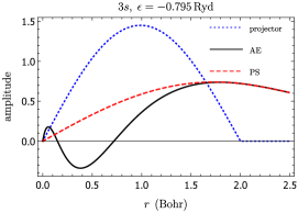
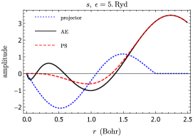
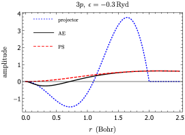
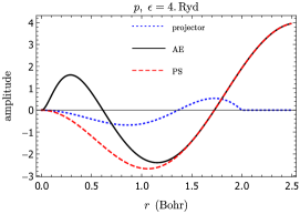
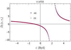


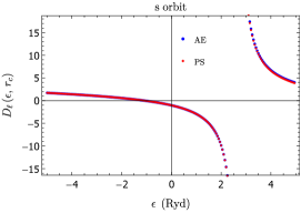

In generation of the PAW datasets of the silicon, the and electrons are taken as the valence electrons, while others in the closed shell are approximated as the frozen core. In Fig. 3.1 we present the partial waves and energy derivatives for the silicon atom, following the recipe. Specifically, we adopt a radius of the augmentation sphere , and two partial waves (so as the projectors) for each angular momentum quantum number and are generated, based on two reference energies of a bound and a scattering states. For , the reference energies are respectively the eigen energies of the bound state () and the scattering state of the silicon atom (). In third row shown are the dimensionless logarithmic derivatives for corresponding AE and PS atomic partial waves, which is defined as
| (3.10) |
where is either the AE partial wave function of Eq. (3.8) at an arbitrary reference energy , or the PS counterpart from the transformed version Eq. (3.6). For large enough augmentation radius , the quantity uniquely determines the phase shifts of the partial waves in scattering theory. Thus the coincidence of the logarithmic derivatives implies that the constructed PAW Hamiltonian well recovers the scattering properties of a single atom, indicating a good performance of the PAW implementation in the energy range of interest.
3.2 Ge
In a parallel fashion, the corresponding partial waves and energy derivatives for the germanium atom are presented in Fig. 3.2. Similarly to case of silicon, the and orbitals are treated as the valence states, while the closed shell is approximated as the frozen core. With radius of the augmentation sphere , two reference energies of the bound orbital () and unbound state () are chosen to generate the partial waves and projectors. For germanium, it is also shown that the logarithmic derivatives of the AE and PS atomic partial waves coincide with each other quite closely.
4 Reconstruction effects on transition event rate
In this section, we first utilize the PAW datasets generated from the code to calculate the band structures of silicon and germanium, as well as both the corresponding AE and PS eigen wave functions with the package GONZE20092582 , from which we then analyze and compare the calculations of relevant DM-induced transition event rates.


Fifteen adjacent bands from both the valence and conduction states across the band gaps are presented in Fig. 4.1 for silicon and germanium, respectively, along a specific Brillouin zone path ---. The valence band maximums (VBM) are rescaled to for convenience, and the band-gap energies , namely, the energies of the conduction band minimums (CBM) are calibrated to the experimental values for silicon () and germanium (), respectively, using the scissor operation. In calculation, we adopt an energy cutoff , a value sufficiently large to obtain converged band structures in the PAW framework. This energy cutoff translates to a cap on the radius of the reciprocal vector at . Moreover, the fast Fourier transformation (FFT) of the electronic density, or square of the wave functions, which makes its appearance in Eq. (LABEL:eq:total_ExcitationRate), requires PW components up to a reciprocal vector radius twice as large as in order to avoid the wrap-around errors. So in practice the charge density is presented in a box consisting of grids. In this work we use the experimental lattice constants for silicon and germanium , respectively.
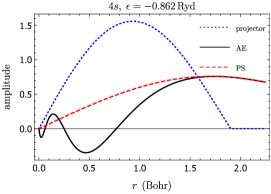
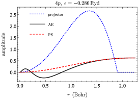
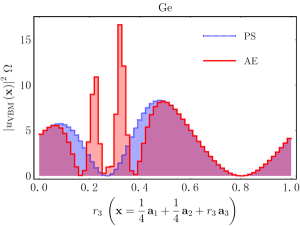
In addition, to illustrate the source of possible error from the pseudopotential method for the calculation of transition event rate Eq. (LABEL:eq:total_ExcitationRate), in Fig. 4.2 we make an elaborate comparison of the valence electron densities between the AE and PS approaches inside the UC. For concreteness, we take the VBM (at the point ) for instance, and choose three specific paths within the UC of the two crystals, which are (in the upper row), (in the middle row), and (in the bottom row) with , respectively, where the primitive vectors are expressed in Cartesian coordinates and in terms of the lattice constant . Corresponding electronic densities are normalized within the UC (see Eq. (2.5)) with condition . As shown in the first and second rows in Fig. 4.2, the AE electronic density (red) features rapid oscillations when the path passes through the nuclei, while outside the augmentation radius the PS density (blue) well coincides with the AE one. When the path does not intersect the augmentation sphere, as shown in the third row, the two wave functions are completely equal.
Another observation from Fig. 4.2 is that the oscillatory behavior of the wave function near the nucleus is so remarkable that the present real grids fall short of resolution to continuously depict the variation details. If the kinetics allows for a large transferred momentum in transition, these highly oscillating wave functions may couple with the high-frequency phase factor terms {} in the expression of transition rate Eq. (LABEL:eq:total_ExcitationRate), and hence more -vector terms can contribute to the total transition rate. The maximum transferred momentum for the given energy difference and DM incident velocity can be drawn from the Heaviside function in Eq. (LABEL:eq:total_ExcitationRate) as the following,
| (4.1) |
In contrast to the case of optical excitation, this massive particle kinetic relation translates to an average momentum transfer of larger given the same transition energy, where represents the typical speed of the galactic DM particles. As a consequence, a larger modulus of -vectors is accordingly required to resolve the short-range details in this deep inelastic scattering process. To get a sense, we take the excitation channel VBMCBM in silicon crystal for instance, where a -DM particle with a typical velocity can produce a transferred momentum as large as , which corresponds to an energy cutoff , far exceeding the typical value of in pseudopotential PW calculations. While these large- phase factors {} decouple from the smooth PS wave functions, they may still resonate with the rapidly oscillatory AE ones.
Therefore, in order to investigate the AE reconstruction effects on the calculation of DM-induced transition rate, we need to choose an appropriate set of parameters in a sense that the maximum momentum transfer should be compatible with the resolution of the real grid adopted in computation. For illustration, we present the largest modulus of integer number vectors for the diamond structure, i.e., 111Given the constraint , where are the primitive reciprocal vectors and are a set of integer numbers, the largest modulus simply equals for the diamond structure. versus two parameters: DM mass and incident velocity , for silicon and germanium crystals in the upper row in Fig. 4.3. The kinetic energy cutoff adopted in this study corresponds to the constraint (in black dashed line) in the implementation of PAW. That is to say, the resolution associated with the cutoff can only describe the electronic excitation processes in colored parameter regions below the black dashed lines in Fig. 4.3, while in the white areas corresponding excitations are kinetically forbidden.
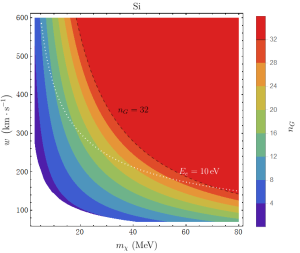


After determining the parameter region compatible with the given energy cutoff, now we can compute the DM-induced electronic excitation rates for the silicon and germanium semiconductor detectors. In calculation we truncate the energy transfer at , which corresponds to including only the transition events from the 4 valence bands to the 7 lowest conduction bands. Such constraint is presented in white dotted lines in the upper row in Fig. 4.3 for silicon and germanium, respectively. Parameters above the white line can induce excitation events with transition energies above , and hence more unoccupied energy bands are required for exact calculation. In addition, although the transition rate Eq. (LABEL:eq:total_ExcitationRate) depends on the orientation of the crystal target with respect to galaxy, for simplicity however, in calculation the velocity distribution is approximated as an isotropic one for parameter , i.e., . Besides, following the strategy in Ref. Essig:2015cda , we equivalently express Eq. (LABEL:eq:total_ExcitationRate) in terms of transferred momentum and energy transfer in order to make the scan of the parameter space computationally more efficient. In short, after inserting the monochromatic velocity distribution the total transition rate for can be recast as
| (4.2) |
for either the AE or the PS wavefunctions, where two reference values for momentum and energy are constructed as and , respectively, is the number of cells in the crystal target, and the non-dimensional form factor is introduced as
| (4.3) | |||||
In realistic computation, several numerical modifications are made to Eq. (4.2) as follows.
-
•
The integrals over and are replaced by the summations over uniform discrete bins of and . We use the bin widths and , and the integrand is evaluated at the central value in each relevant bin. The delta functions are discretized to a normalized step function. For example, if a specific parameter falls into the -th energy bin, then the function is approximated as , with being the central value of this bin.
-
•
As a standard DFT numerical procedure, the integrals of the continuous -points in the first BZ are replaced by the summations over a uniform discrete mesh of representative -points in the following manner:
(4.4) where is the number of -points sampled in the first BZ. In this study, we use a homogeneous set of -points.
-
•
Integral can be understood as the Fourier transformation of the square term within the UC, which is practically performed using the discrete FFT technique, so the reciprocal -vectors have a natural truncation consistent with the grid number in the real space. As mentioned above, the modulus number of the -vectors can extend to a value no more than 32 in our analysis.
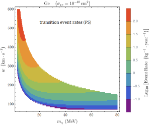
In the middle row of Fig. 4.3, we present the calculated transition event rates per kilogram-day from the PS wavefunctions for silicon (left) and germanium (right), respectively. A DM-electron cross section is assumed, and only the parameter regions below the transition energy constraint (white dotted line in the upper row) and the -vector bound (black dashed line in the upper row) are calculated. In the bottom row shown are the comparisons between the theoretical excitation event rates derived from the AE and PS approaches for the two crystals, in terms of the ratio of the AE event rate to its PS counterpart for each parameter pair and , i.e., . In large part of the scanned region, the two calculated even rates are found to be quite consistent. Interestingly, however, in areas where large momentum transfer (or equivalently, large ) can be induced, the estimates based on the AE and PS approaches begin to differ with each other, and this trend seems to continue into larger -vector parameter region. Therefore, the actual electronic distribution near the nucleus is of remarkable relevance for the estimation of the DM-induced excitation rate, especially in the area where a large momentum transfer is favored in the excitation process.


In order to demonstrate the origin of such deviation, in Fig. 4.4 we present the comparison of the form factor in Eq. (4.2), between the AE and PS approaches for silicon. This non-dimensional quantity is convenient for direct contrast because all the integrand function values in pixels are accounted with equal weight when summed up to obtain the total event rate. The momentum transfer is expressed in terms of the silicon reciprocal lattice . We choose two benchmark points representative of two distinct scenarios in the bottom row of Fig. 4.3, i.e., when the AE-based estimate of event rate differs with its PS counterpart, and when the AE-based estimate of event rate agrees with its PS counterpart.
For the first case, we take the parameter pair , as example. At this point one has , and the kinetics confines the integration in Eq. (4.2) within the area in the red contour in Fig. 4.4, only where the Heaviside step function yields non-zero value. In addition, an important observation from Fig. 4.4 is that as we expected, the AE wavefunctions near the nucleus, reconstructed from the PAW transformation Eq. (3.4), indeed play a non-negligible role in transitions where large transferred momentum participates. While the PS approach gives an accurate description of the excitation process in the parameter area below , (which is referred to as small- region, and the rest area is referred to as large- region, for convenience) the relevant form factor falls off so rapidly towards the large- region that the PS scheme may cause remarkable error in the calculation of event rates. Comparing the AE case (left) to the PS one (right), one finds that the large ratio can be attributed to the fact that the contour on one hand covers only a small portion of the parameter area where the PS-based description remains effective, and on the other it contains a sizable part of the large- parameter area. These two factors effectively enchance the contrast.
As for the other case, we pick the parameter pair , () for illustration. Since half of the kinetically allowed region (contoured in blue line) overlaps the small- area, based on the above reasoning, it is understandable that the corrections from the AE approach are not so remarkable under this circumstance. Moreover, the galactic DM velocity distribution also imposes a kinetic constraint on the - plane. Actually, given the truncated Maxwellian distribution introduced in Sec. 2, and the fact that the reaches its minimum as (see Eq. (2.4)), the minimal kinetically accessible transferred momentum for recoil energy equals , which corresponds to the yellow dashed line presented in Fig. 4.4. The region below the line is kinetically forbidden. The implication is that large recoil energy requires large momentum transfer accordingly, and thus an accurate description of the AE electronic wave functions becomes necessary.
5 Conclusions and discussion
In this work, we have investigated the implications of the PAW reconstruction procedure on the estimation of electronic transition event rate in two most common semiconductor targets used in the DM direct detection, namely, silicon and germanium semiconductors. By use of the PAW method, one can restore the AE electronic wavefunctions from the PAW PS wavefunctions without much extra computational loads. To this end, we first utilize the code to generate appropriate PAW datasets including the PAW pseudopotential, and input these files into the package to compute the electronic structure and relevant AE and PS wavefunctions. Based on the wavefunctions, we then calculate relevant DM-induced excitation event rates and make comparisons between the AE and PS approaches. It is found that the PS approach turns inapplicable in describing excitation processes involving large transferred momentum, because the oscillating components that would couple with large momentum transfer are deliberately spared in calculation. Even in the limited parameter region scanned in our study, the two calculated event rates are found to differ with a factor of two. So this work serves as a caveat in relevant calculations that an accurate estimate of the DM-induced transition event rate should better be implemented with the AE approaches.
Similar experimental strategies can be extended to the detection of the sub-MeV DM particles. For instance, in Ref. Hochberg:2017wce the authors discussed the theoretical prospects for detecting sub-MeV DM particles by use of the three-dimensional Dirac materials with typical band gap meV. Discussion of the AE reconstruction effects can also be applied parallelly to this case. However, considering the dependence of maximum momentum transfer on the DM mass at the sub-MeV scale (see Eq. (4.1)), the high-momentum PWs from reconstruction do not contribute to the transition event rates, so in such case the reconstruction effects are expected to be insubstantial.
Finally, a thorough estimate of the total event rate should involve convoluting with the realistic DM velocity distribution, and thus requires a broader recoil energy range and a larger energy cutoff (see Fig. 4.3), which unfortunately, is beyond the capabilities of our cottage-industry work style. As a more efficient solution, computation of the crystal form factor should be processed within the well-established software packages, e.g., in this study. We leave it for future work.
Acknowledgements.
ZLL thanks Xingyu Gao for useful discussions. PZ is supported by the Science Challenge Project No. TZ2016001, and NSFC No. 11625415. FZ acknowledges the support by China PFCAEP under the Grant No. YZJJLX2016010. The computations are supported by Beijing Computational Science Research Center (CSRC) and HPC Cluster of ITP, CAS.References
- (1) M. W. Goodman and E. Witten, Detectability of Certain Dark Matter Candidates, Phys. Rev. D31 (1985) 3059. [,325(1984)].
- (2) XENON100 , E. Aprile et al., XENON100 Dark Matter Results from a Combination of 477 Live Days, Phys. Rev. D94 (2016), no. 12 122001, [ arXiv:1609.06154].
- (3) LUX , D. S. Akerib et al., Results from a search for dark matter in the complete LUX exposure, Phys. Rev. Lett. 118 (2017), no. 2 021303, [ arXiv:1608.07648].
- (4) PandaX-II , A. Tan et al., Dark Matter Results from First 98.7 Days of Data from the PandaX-II Experiment, Phys. Rev. Lett. 117 (2016), no. 12 121303, [ arXiv:1607.07400].
- (5) EDELWEISS , Q. Arnaud et al., Optimizing EDELWEISS detectors for low-mass WIMP searches, Phys. Rev. D97 (2018), no. 2 022003, [ arXiv:1707.04308].
- (6) SuperCDMS , R. Agnese et al., Search for Low-Mass Weakly Interacting Massive Particles with SuperCDMS, Phys. Rev. Lett. 112 (2014), no. 24 241302, [ arXiv:1402.7137].
- (7) R. Essig, J. Mardon, and T. Volansky, Direct Detection of Sub-GeV Dark Matter, Phys. Rev. D85 (2012) 076007, [ arXiv:1108.5383].
- (8) P. W. Graham, D. E. Kaplan, S. Rajendran, and M. T. Walters, Semiconductor Probes of Light Dark Matter, Phys. Dark Univ. 1 (2012) 32–49, [ arXiv:1203.2531].
- (9) R. Essig, M. Fernandez-Serra, J. Mardon, A. Soto, T. Volansky, and T.-T. Yu, Direct Detection of sub-GeV Dark Matter with Semiconductor Targets, JHEP 05 (2016) 046, [ arXiv:1509.01598].
- (10) S. K. Lee, M. Lisanti, S. Mishra-Sharma, and B. R. Safdi, Modulation Effects in Dark Matter-Electron Scattering Experiments, Phys. Rev. D92 (2015), no. 8 083517, [ arXiv:1508.07361].
- (11) P. Hohenberg and W. Kohn, Inhomogeneous electron gas, Phys. Rev. 136 (Nov, 1964) B864–B871.
- (12) W. Kohn and L. J. Sham, Self-consistent equations including exchange and correlation effects, Phys. Rev. 140 (Nov, 1965) A1133–A1138.
- (13) P. Giannozzi, S. Baroni, N. Bonini, M. Calandra, R. Car, C. Cavazzoni, D. Ceresoli, G. L. Chiarotti, M. Cococcioni, I. Dabo, A. D. Corso, S. de Gironcoli, S. Fabris, G. Fratesi, R. Gebauer, U. Gerstmann, C. Gougoussis, A. Kokalj, M. Lazzeri, L. Martin-Samos, N. Marzari, F. Mauri, R. Mazzarello, S. Paolini, A. Pasquarello, L. Paulatto, C. Sbraccia, S. Scandolo, G. Sclauzero, A. P. Seitsonen, A. Smogunov, P. Umari, and R. M. Wentzcovitch, Quantum espresso: a modular and open-source software project for quantum simulations of materials, Journal of Physics: Condensed Matter 21 (2009), no. 39 395502.
- (14) Y. Hochberg, T. Lin, and K. M. Zurek, Detecting Ultralight Bosonic Dark Matter via Absorption in Superconductors, Phys. Rev. D94 (2016), no. 1 015019, [ arXiv:1604.06800].
- (15) Y. Hochberg, Y. Kahn, M. Lisanti, C. G. Tully, and K. M. Zurek, Directional detection of dark matter with two-dimensional targets, Phys. Lett. B772 (2017) 239–246, [ arXiv:1606.08849].
- (16) Y. Hochberg, T. Lin, and K. M. Zurek, Absorption of light dark matter in semiconductors, Phys. Rev. D95 (2017), no. 2 023013, [ arXiv:1608.01994].
- (17) Y. Hochberg, Y. Kahn, M. Lisanti, K. M. Zurek, A. G. Grushin, R. Ilan, S. M. Griffin, Z.-F. Liu, S. F. Weber, and J. B. Neaton, Detection of sub-MeV Dark Matter with Three-Dimensional Dirac Materials, Phys. Rev. D97 (2018), no. 1 015004, [ arXiv:1708.08929].
- (18) G. Cavoto, F. Luchetta, and A. D. Polosa, Sub-GeV Dark Matter Detection with Electron Recoils in Carbon Nanotubes, Phys. Lett. B776 (2018) 338–344, [ arXiv:1706.02487].
- (19) S. Knapen, T. Lin, M. Pyle, and K. M. Zurek, Detection of Light Dark Matter With Optical Phonons in Polar Materials, arXiv:1712.06598.
- (20) S. Knapen, T. Lin, and K. M. Zurek, Light Dark Matter: Models and Constraints, Phys. Rev. D96 (2017), no. 11 115021, [ arXiv:1709.07882].
- (21) S. Griffin, S. Knapen, T. Lin, and K. M. Zurek, Directional Detection of Light Dark Matter with Polar Materials, arXiv:1807.10291.
- (22) T. Liang, B. Zhu, R. Ding, and T. Li, Direct Detection of Axion-Like Particles in Bismuth-Based Topological Insulators, arXiv:1807.11757.
- (23) B. Adolph, J. Furthmüller, and F. Bechstedt, Optical properties of semiconductors using projector-augmented waves, Phys. Rev. B 63 (Mar, 2001) 125108.
- (24) P. Delaney, B. Králik, and S. G. Louie, Compton profiles of si: Pseudopotential calculation and reconstruction effects, Phys. Rev. B 58 (Aug, 1998) 4320–4324.
- (25) I. Makkonen, M. Hakala, and M. Puska, Calculation of valence electron momentum densities using the projector augmented-wave method, Journal of Physics and Chemistry of Solids 66 (2005), no. 6 1128 – 1135.
- (26) D. R. Hamann, M. Schlüter, and C. Chiang, Norm-conserving pseudopotentials, Phys. Rev. Lett. 43 (Nov, 1979) 1494–1497.
- (27) D. Vanderbilt, Soft self-consistent pseudopotentials in a generalized eigenvalue formalism, Phys. Rev. B 41 (Apr, 1990) 7892–7895.
- (28) P. E. Blöchl, Projector augmented-wave method, Phys. Rev. B 50 (Dec, 1994) 17953–17979.
- (29) G. Kresse and D. Joubert, From ultrasoft pseudopotentials to the projector augmented-wave method, Phys. Rev. B 59 (Jan, 1999) 1758–1775.
- (30) N. Holzwarth, A. Tackett, and G. Matthews, A projector augmented wave (paw) code for electronic structure calculations, part i: atompaw for generating atom-centered functions, Computer Physics Communications 135 (2001), no. 3 329 – 347.
- (31) J. P. Perdew, K. Burke, and M. Ernzerhof, Generalized gradient approximation made simple, Phys. Rev. Lett. 77 (Oct, 1996) 3865–3868.
- (32) X. Gonze, B. Amadon, P.-M. Anglade, J.-M. Beuken, F. Bottin, P. Boulanger, F. Bruneval, D. Caliste, R. Caracas, M. Cote, T. Deutsch, L. Genovese, P. Ghosez, M. Giantomassi, S. Goedecker, D. Hamann, P. Hermet, F. Jollet, G. Jomard, S. Leroux, M. Mancini, S. Mazevet, M. Oliveira, G. Onida, Y. Pouillon, T. Rangel, G.-M. Rignanese, D. Sangalli, R. Shaltaf, M. Torrent, M. Verstraete, G. Zerah, and J. Zwanziger, Abinit: First-principles approach to material and nanosystem properties, Computer Physics Communications 180 (2009), no. 12 2582 – 2615.