Impact of thermal transport parameters on the operating temperature of OLEDs
Abstract
Excess heat in organic light emitting diodes (OLEDs) that is produced during their operation may accelerate their degradation and may cause an inhomogeneous brightness distribution, in particular in large area OLEDs. Assessing the quantitative impact of heat excess is difficult, because all decisive processes related to charge transport and emission via charge recombination are thermally activated. For example, electric currents that are elevated due to larger temperatures cause additional Joule heating and increase, hence, the device temperature even further. Here we establish how parameters responsible for heat transport, i.e., the thermal conductivity of the organic layers and the heat transfer coefficient between the device surface and the environment govern the temperature inside the OLED. We establish, relying on three-dimensional drift-diffusion simulations that self-consistently couple thermally-activated charge transport and heat transport, that the thermal conductivity of organic layers is not a bottleneck for heat transport, because the encountered layer thicknesses in realistic device geometries prevent heat accumulation. The heat transfer to the ambient environment is the key parameter to dissipate excess heat from the device. Intentionally elevated operating temperatures, that may improve the OLEDs electric performance, are not necessarily beneficial, as any increase in operating temperature decreases the device stability. The thermal effects being decisive for the OLED temperature occur in device layers beyond the electrically active region. We propose analytical expressions that relate the temperature in the device for a given point of operation to the heat transfer to the environment and the substrate.
pacs:
73.21.Ac; 73.40.Lq; 73.50.Lw; 73.61.Ph; 81.05.Fb; 85.30.DeI Introduction
Two major factors presently hinder the application of organic light emitting diodes (OLEDs) for large-area lighting applications: device degradation and inhomogeneous light emission from the exterior surface.Park et al. (2011b) Both factors strongly relate to excess heat that is generated during operation. On the one hand, elevated temperatures inside the OLEDs accelerate degradation,Xu and Xu (2004); Zhou et al. (2000); Nenna et al. (2007) alongside with other factors such as water penetrating into the device Li et al. (2016), surface roughness, and mass diffusion of material. On the other hand, local variations in temperature and, hence, in the in-plane current density give rise to an inhomogeneous brightness distribution.Gärditz et al. (2007); Kohári et al. (2013) The primary origin of such locally elevated current densities and temperatures are non-uniformly distributed driving voltages, because these voltages differ due to position-dependent ohmic losses in the large area contacts.Fischer et al. (2014) As a consequence, the efficiency of how heat is dissipated from the device becomes dependent on the position in which the heat is generated. Even if heating is compensated by heat outflow,Park and Lee (2014) such instabilities may lead to local ”bright spots” in which the device will degrade much faster.
The quantitative impact of heat excess is particularly difficult to assess, because the major effects that govern the electrical performance are thermally activated, i.e., the charge transport and the recombination efficiency in the organic layers. An increasing temperature enlarges the charge carrier mobility in organic thin filmsBässler (1993) and the recombination rates and, hence, increases the device current. In turn, this enhanced current causes larger Joule heating and elevates the temperature even further. If this process of self-activated heating is balanced by a sufficient outflow of heat, the current reaches a stable steady state. Unbalanced, the self-activated heating process can drive the device into a ”vicious cycle”, which will eventually overheat the device to the point where it is not operable anymore.
In this article, we pursue the question how the parameters that are responsible for heat transport in OLEDs govern the temperature distribution in the device. Inspired by the vast efforts spent to optimize the material properties for charge transport, our article focuses on the thermal properties that most favorably support the device operation. Specifically, we seek to learn (i) whether the parameters that govern heat transport represent separate tuning handles to dissipate heat, and (ii) with which layers of the OLED stack the heat dissipation can be efficiently controlled. As further asset we seek to determine a relation between the device temperature, the electric current, and the heat transport parameters. With such a relation, even if approximate, we would be able to predict how the OLED operation is affected by its thermal transport properties and able to estimate the impact of heat dissipation directly from an experimentally obtained current voltage characteristics.
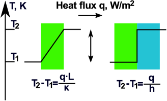
As a first parameter, we consider the thermal conductivity of individual organic layers. As illustrated in Figure 1, describes how efficient heat is transported from the heat source through a layer of a thickness . The second considered parameter is the heat transfer coefficient that describes heat transport through an interface (Figure 1).Jin et al. (2014) In the context of OLEDs, the heat transfer coefficient between the outermost layers and the ambient environment appears to be most crucial. There are clear indications that the heat outflow from the device can be sufficiently improved by choosing an appropriate substrate.Chung et al. (2009); Triambulo and Park (2016) As the generated heat has to be dissipated with respect to ambient temperature, the absolute temperature within the organic layers will be influenced not only by the electric current, but also by the ambient temperature.
We employ drift-diffusion based simulations to monitor how these two types of parameters, i.e., and , contribute to the thermal and electrical behavior of the OLED. With such simulations, we simultaneously account for charge and heat transport based on the (i) geometry of the OLED stack, (ii) the material parameters governing the charge and the thermal transport, and (iii) the coupling between charge and heat transport to establish a self-consistent feedback between them. This allows us to obtain current-voltage characteristics and temperature-voltage relation for an OLED that is operated at a given ambient temperature.
II Methodology
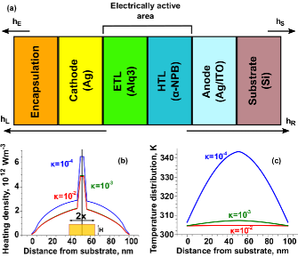
To efficiently model the charge and heat transport, we distinguish between two device regions, i.e., (i) the region in which heat is generated, and (ii) in device regions, in which solely heat is transported. These regions are reflected in the schematic OLED cross section in Figure 2 as follows: In the organic layers between the electric contacts, the electric current produces both Joule heating and heating due to non-radiative recombination. Hence, the region comprising the organic layers and the contacts will be described with a three dimensional drift-diffusion model for coupled charge and heat transport.
In the regions outside the contacts, i.e., in the encapsulation and substrate layers, no further heat is produced. In the absence of electric current, it is sufficient to solve the heat transport equation. The latter equation can be solved analytically for steady state operation, sparing us to solve the heat transport equation for the entire device with the elaborate numerical approach necessary for the electrically active region. For convenience, the OLED cross-section shown in Figure 2 is oriented such that the layers are stacked along the z-axis and laterally extended in the x-y plane. In this orientation, the externally applied voltage shall be uniformly applied between cathode and anode, i.e., the voltage drops in z-direction and is uniform in x and y directions.
II.1 Drift diffusion model
The drift-diffusion model is an established approach for the investigation of the electrical performance of OLEDs.Davids et al. (1997); Knapp et al. (2010); Knapp and Ruhstaller (2011); Ruhstaller et al. (2003); Slawinski et al. (2011); van Mensfoort and Coehoorn (2008) Since the model describes transport processes with effective material parameters, the model can be straight-forwardly extended to consider also heat transport and thermoelectric effects.Park et al. (2011a)
All charge densities, energy densities, and material parameters are dependent on the position in the device, so that the fluxes of the thermal energy and charges are three component vectors. Below we describe the formulation and the implementation of the fully three dimensional drift-diffusion model. Such a consideration of three-dimensional fluxes and related density distributions is crucially required to address lateral variations in temperature and in-plane current densities. Hence, we are aiming at devising a simulation code with which one can address temperature-related inhomogeneity issues that are beyond the scope of this work.
In general, charge and heat transport are governed by two types of equations, the continuity equations and the current density equations. The continuity equations for the densities of mobile charges, i.e., of electrons, , and holes, , and the density of thermal energy, , read:
| (1a) | |||
| (1b) | |||
| (1c) | |||
Therein, and are the electron and hole flux (rather than the electric current densities) respectively, and the generation and recombination rates. We are using the Langevin recombination model.Langevin (1903) Note that there are more refined models to account for recombination rates which, however, would introduce additional free parameters to the our description.Lee et al. (2014); van der Holst et al. (2009) In Eq. 1c, refers to the temperature, to the mass density, to the specific heat capacity, and to the heat flux. The term accounts for the amount of heat energy added or abstracted per unit volume and per unit time. The current density equations connect the fluxes with the densities:
| (2a) | |||
| (2b) | |||
| (2c) | |||
Eqs. (2a,2b) contain the material parameters responsible for charge transport, i.e., is the mobility of the corresponding charge carriers, the diffusion constant, and the Seebeck coefficient. Eq. (2c) formulates the Fourier law and contains the heat conductivity . To account for the hopping nature of the transport in organic materials, we consider mobilities and a Seebeck coefficient that depend on electric field, temperature, and charge carrier concentration. There are different methods to incorporate this dependencies,Fishchuk et al. (2010, 2013) we use relations that were previously extracted from Monte Carlo simulations.Lu et al. (2015); Pasveer et al. (2005)
The current densities and across organic-organic heterojunctions are also treated with Eqs. (2a,2b). Besides drift and diffusion, we introduce an additional driving force for electrons and for holes at the position of the heterojunction. The extent of this force reflects how the transport-relevant levels of the two organic materials align at the heterojunction. We obtain this force from a generalized electrostatic potential, , that contains two additional terms compared to the actual electrostatic potential . The first term accounts for the difference in the nominal transport level energies and of the two materials by introducing an additional potential drop across the heterojunction, i.e., for holes and for electrons, respectively.E. Sutherland and R. Hauser (1977) The second term accounts for the fact that the density of states available for hopping transport is changing across the heterojunction. We cast this change in the density of states into a local contribution to the generalized electrostatic potential following the argumentation in Ref. Liemant (1997). The current densities and entering and leaving the OLED across the contacts are described by a net injection current. This injected current is a superposition of different contributions that are associated to the offset between the transport levels and the workfunction of the electrode metal, forming the injection barrier. We specifically consider current density contributions due to thermionic and tunneling injection (from contact into organic layer) as well as interface recombination (from organic layer into the contact).Davids et al. (1996); Gruber et al. (2012); Scott and Malliaras (1999) The individual contributions are self-consistently determined as a function of the local situation present at each contact during operation. Particularly important are the temperature (thermionic injection) and the local electric field (thermionic and tunneling injection).
The local electric field that drives the charges is given as the gradient of the electrostatic potential . At heterojunctions, this field is replaced by an effective field related to the generalized electrostatic potential . The potential is connected to the local net charge density via the Poisson equation
| (3) |
in which is relative dielectric permittivity and the vacuum permittivity. The potential set at the cathode corresponds to the applied voltage , while the potential at the anode is set to zero.
The heat flow across the organic-organic heterojunction is considered in Eq. (2c) via a thermal conductivity that is averaged with respect to the of the layers meeting at the interface. The heat flow is directed out of the device, i.e., at , if the temperature in the device exceeds the ambient temperature. The heat flow out of the contacts, i.e., the flow leaving the region in which heat is generated, is assumed to be proportional to the difference in the temperature of the contact surface, e.g., at , and the ambient environment :
| (4) |
Therein, an effective heat transfer coefficient dictates, how well the contact at is thermally connected to the ambient environment. Analogously, we also assume an effective heat transfer coefficient for the contact surface at (Fig. 1). The higher the heat flux through the contact interface is, the higher is the temperature gap between the contact surface and the ambient. The effective heat transfer coefficients , are directly related to the propagation of heat through the subsequent layers between the respective contact and the environment. As will be explained in the section ”Analytic solution of the heat equation” below, we can express and in terms of all thermal layer properties that connect the contact surfaces to the ambient environment, i.e., the of the individual layers, the coefficients between these layers, and the heat transfer coefficients and between the outermost encapsulation and substrate layer to the ambient. With this definition, , enable us to monitor directly the heat exchange between the electrically active layers and the ambient environment acting as heat sink.
The system of equations (1,3) with the above-stated boundary conditions is solved in the regions of the organic semiconducting layers. Periodic boundary conditions are imposed along the spatial directions perpendicular to the stacking direction. We discretized the equations (1,3) with the Finite Differences Method on a non-uniform rectangular 3D mesh (for drift-diffusion equation we use the Scharfetter-Gummel discretization scheme Scharfetter and Gummel (1969)) and solved them iteratively with an explicit time discretization scheme (Euler forward) until steady state was achieved. The solving algorithm was implemented in Fortran 95 and uses Open MPI to parallelize the computation.
For our problem at hand, it is sufficient to consider only one spatial dimension, i.e., using a 1x1xN grid to discretize the cross-section shown in Figure 2-a. This is, because here the potential drop across the device is assumed to be independent from the lateral position in the contact surface. We carefully tested multiple devices with varying lateral extensions to ensure that the results from the one-dimensional simulations coincide with the ones obtained on a three-dimensional grid. Furthermore, we verified that the simulations converged to a steady state that did not depend on the initial conditions assumed in the simulations.
II.2 Analytical solution to the heat transfer equation
Outside of the electrical contacts, the temperature distribution corresponds to the solution of the steady-state heat equation. Since the voltage is constant in both lateral directions, i.e., perpendicular to the stack axis, we anticipate a temperature variation only along the stack. The temperature distribution for steady state operation is correspondingly given by the one-dimensional, the steady-state heat equation (cf. Eq. (1c)):
| (5) |
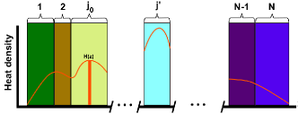
The source term on the right hand side contains the heat generation profile . The general analytic solution of Eq. (5) can be obtained with a Greens function approach for an arbitrary layer sequence and for an arbitrary, static heat generation profile. Such a sequence is indicated in Figure 3.
Note that Eq. (5) can be solved in terms of discretized slices being considerably thinner than the actual layers. However, such a refined discretization is usually necessary only if the heat generation profile is non-uniform. The full expressions for the solution are given in the Supporting Information.
With the general steady-state solution at hand, we can construct the effective heat transfer coefficients and that represent the thermal transport behavior of all layers between the ambient environment and the electrical contacts. and will serve as boundary conditions for the heat equation that is solved in the region between the contacts. Since we presume that the heat is exclusively generated in the region between the contacts and that this heat flows out of the device, we can interpret as the total thermal resistance due to all layers the thermal flux had to pass through on its way to respective edge of the device. Such substrate- or encapsulation-sided thermal resistances consist of the sum of all individual thermal resistances that are located between the contact and the ambient environment, be them due to (i) the heat transfer coefficient at each interface between layers and or due to (ii) the thermal conductivities in each layer . Recalling that is the thermal transport coefficient of the interface between the outermost encapsulation (/substrate) surface and the ambient environment, we get:
| (6) |
II.3 Device layout
A major challenge for the simulation of the transport through the layers and across the layer interfaces is the large number of required parameters. Each layer requires the heat conductivity and a set of parameters that describe charge transport. Each pair of interfaces requires parameterized conditions that ensure charge and energy conservation, such as heat transfer coefficients and injection currents. An unbiased systematic variation of all these parameters yields only limited insight and does not provide leads for relevant relations without generating a very large set of data. Therefore, we seek a model device for our simulations, that serves three purposes: (i) The device layout should support the setup of a toy model with which the role of the heat transfer coefficients towards the environment and the heat conductivities of the organic layers can be conveniently distinguished. (ii) The toy model should operate with a strongly reduced amount of parameters so that the impact of charge and heat transport can be disentangled best. (iii) It must be possible to straight-forwardly extent our toy model to accommodate more involved device structures with our modeling methodology.
Figure 2-a shows a cross-section of a suitable device. While state-of-the-art devices contain a large number of distinct layers, we explicitly consider here two organic layers in which either predominantly hole or electron transport takes place. The two organic semiconducting layers are sandwiched between an anode and a cathode. The organic layer adjacent to the cathode assumes the role of a electron transport layer while the one adjacent to the anode preferentially transports holes. The division into two organic layers that form a heterojunction allows us to account for multiple conceivable charge transport scenarios in an effective manner. Elaborate stacks for encapsulation or substrates are accounted for in this cross-section by one substrate and one encapsulation layer to capture their characteristic thickness and thermal properties. In general, however, the thermal behavior of the full sub-stacks that are not electrically active can be cast into effective heat transfer coefficients.
In a next step, we construct the device to be symmetric from a thermal point of view, because this symmetry halves the amount of free parameters necessary to describe thermal and charge transport. As there is no differentiation between top (encapsulation) and bottom (substrate) anymore, we can use a common effective heat transfer coefficient rather than distinguishing between and . To guarantee the desired symmetric distribution of the heat density, two conditions must be fulfilled. Firstly, the layers left and right of the device center must have equal thermal conductivities . With having reduced our thermal parameters to and , we can more clearly track their impact on the device temperature and performance. Secondly, also the electric current density responsible for heat generation must be equal in the layers left and right of the device center. This condition of balanced current halves the amount of necessary electrical parameters. If realistic parameters are imposed for one layer, only parameters of the second layer require an adjustment to balance the current. In practice, the adjusted parameters are either the electron or the hole mobility in their respective transport layer or the offset between either the electron or the hole transport levels. A prototypical symmetric heating profile is shown in Figure 2-b. We propose that such symmetric devices are ideal starting points to monitor the impact of subtle changes in the coupling between charge and heat transport.
II.4 Material and geometry parameters.
If not otherwise specified, we use the following parameters to setup our symmetric model OLED. Each organic layer in our symmetric model device is 50 nm thick. The parameters for the electron transporting layer are inspired by Alq3 and for the hole transporting layer by -NPB. The offset between the electron transport levels is 0.3 eV, the offset between the hole transport level is the same. In each layer, the charge that is preferentially transported is considered with a charge carrier mobility , whereas the charge of opposite polarity is considered with . The mobilities are and , regardless whether electrons or holes are concerned. In the simulation, these mobility values correspond to the limit that the mobility attains for low electric fields and low charge carrier densities at room temperature. The relative dielectric permittivity = 3.5. We disregard a direct thermoelectric coupling in our simulations by setting the Seebeck coefficient to zero. Considering the typical values of in organic semiconductors, the related thermal voltages are small compared to the applied voltage. With this premise, the Seebeck coefficient has a negligible effect on the temperature and charge distribution and its disregard speeds up the simulations. We are using for both organic layers a mass density and a heat capacity . Note that mass density and heat capacity will not affect the steady state according to Eq. (1c); rather, they affect the time scale in which steady state is reached. Thermal conductivities of the organic layers realistically varyReisdorffer, Frederic et al. (2014) between . They are inferior to the thermal conductivity of ordinary glass, ( = 1.022 for a glass cover).
III Impact of thermal properties on the OLED operation
III.1 Contributions to heating
As a starting point, we explore how the generated heat is distributed across our symmetric model OLED operated at = 5V and at room temperature = 300 K. Characteristic heat density distributions for three different values of = , , and are shown in Fig. 2-b. Regardless of the values of and , these distributions are inherently symmetric with respect to the device center and consist of two distinct contributions. (i) The heat density features a sharp peak at the center. This contribution arises from the non-radiative electron-hole recombination that is localized at the organic-organic heterojunction. (ii) Joule heating is caused by the flow of charge carriers and stretches essentially throughout the entire cross-section. The largest amount of Joule heat is produced in the center, where the electric field that drives the current is highest. Correspondingly, the heat density drops from the center towards the contacts.
The temperature distribution across the OLED is shown in Fig. 2-c. Inherent to the symmetric profile of the generated heat, the temperature attains its maximum in the device center at the heterojunction. This maximum temperature depends on the value . However, only for a as low as 10-4 a maximum temperature is established that significantly exceeds the ambient temperature (by 40 K).
III.2 Heat transfer coefficient vs. thermal conductivity
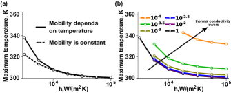
To systematically clarify, how the temperature distribution changes with and for a given voltage, we performed simulations in which the values of the thermal conductivities and heat transport coefficients varied by several orders of magnitude. To learn which combinations of and lead to realistic and significant temperature elevations (from 1 to 100 K above room temperature), we intentionally also incorporated values for and that materials cannot necessarily attain. The maximum temperature taken from the simulated temperature distributions is shown as a function of for several values of in Figure 4.
Elevated maximum temperatures occur if either or are small. Small values of and correspond to a situation, in which we reduce the ability to dissipate heat from the OLED and, hence, store more heat inside the device. The stored heat results in a strongly elevated temperature, as seen for in Figures 4-a,b. Note that the temperature elevation is particularly driven by the thermally activated charge transport. As shown in Figure 4-a, the attained maximum temperature is considerably larger compared to a hypothetical situation with a temperature-independent mobility. The thermal conductivities of the organic layers in the OLEDs, expected to be between 0.1 and 1 , have a negligible impact on the temperature; the associated temperatures in Figure 4-b are indistinguishable. Even when taking a seriously underestimated thermal conductivity of 0.01 W/mK, the corresponding temperature distribution in Fig. 2-b (red line) exceeds the ambient temperature by less than 4 K. This rather unexpected, negligible impact of roots in the fact that the typical thickness of the electrically active layers is not large enough to sustain a temperature gradient inside the layer. To see this, we develop the following rationale:
For our device consisting of two electrically active organic layers, we determine the highest, , and the lowest temperature, , inside the OLED with the help of the steady state heat flow equation (Eq. (5)) for given operating conditions. These solutions and are then interpreted in terms of and . The maximum temperature serves us as an indicator, how well the materials and operating conditions support the heat dissipation from the device. Combining with , we also get largest temperature difference with the device. To ease a subsequent interpretation, we approximate the heat density distribution with a centered uniform profile . Choosing the extension of the uniformly heated region to be (cf. Fig. 2-b), the totally heat generated with this profile is . The lowest temperature is adopted on the device surfaces, . Given the arc-like shape of the temperature distribution (cf. Fig. 2-c), that is symmetric for our model devices, is located in the center of the device = . Hence, we get and from the general solution of the steady state heat flow equation Eq. (5) (cf. Supporting Information for full expression) at and , respectively:
| (7a) | ||||
| (7b) | ||||
Both temperatures are proportional to the total heat generated in the device, . The surface temperature is inversely proportional to , but does not contain any dependence on the thermal conductivities of the electrically active layers. The temperature is determined by two terms, one being inversely proportional to and one being inversely proportional to the thermal conductivity . This second term conveys two important insights: Firstly, the thermal conductivity influences the lesser, the less concentrated the generated heat profile is, i.e., the smaller the difference between the thickness of the layers and the halfed extension of the heat density profile is. Secondly, even in a best-case estimation, in which we insert realistic values = 150 nm and = 0.1 , remains with 1.5 at least an order of magnitude smaller than the 1/ contribution. The thermal conductivity of the organic materials would non-negligibly contribute to if the organic films were at least a factor of ten thicker.
At this point, the irrelevance of the thermal conductivity for thermal transport in realistically thin organic films has two important consequences. Firstly, the actual bottleneck for heat dissipation is the combined thermal transfer between the contacts and the exterior, i.e., the thermal conductivities of layers being not electrically active and the associated heat transfer coefficients. Vice versa, the layers that are responsible for electric transport are not relevantly involved in heat dissipation. This implies that the thermal and electrical properties can be optimized independent from each other in complementary regions of the device to reach a desired performance. Secondly, the temperature within the organic layers is uniform, i.e., = = const. Then, can be immediately related to the total amount of generated heat per unit area, , via the heat balance equation :
| (8) |
Note we do not require a symmetric device to establish this relation. equals in the case of a rectangular heating profile. The heat transfer from the contacts to their associated device surfaces is fully accounted for in the effective heat transfer coefficients and .
III.3 Impact of heat transfer on the current-voltage characteristics
With having established that the thermal conductivity has a negligible impact on the device temperature, we turn to a closer inspection of the role of .
If the maximum temperature is already markedly elevated, as seen in Figure 4 for the smaller , small changes in cause a large change in the temperature. This finding is potentially relevant if one considers to operate the OLED considerably above room temperature, as such elevated temperatures promote the electric conduction and radiative recombination. Subtle changes in the OLED layout, e.g., in terms of the thickness of the encapsulation layer, may strongly alter the temperature in the device, possibly even pushing the device in the regime of insufficient cooling and, concomitantly, into self-heating and thermal run-away.
In a next step we explore how affects the electric current and heating for different applied voltages. To obtain a current-voltage characteristic, we computed the current for each external voltage anew starting out from an operating temperature equal to the ambient temperature. Hence, the computed I-V curves correspond to electric measurements that allow the device to sufficiently cool between consecutive current acquisitions.
Figure 5-a shows the current of the symmetric model OLED with = 1 and = 105 operated at room temperature = 300 K a function of the applied voltage.
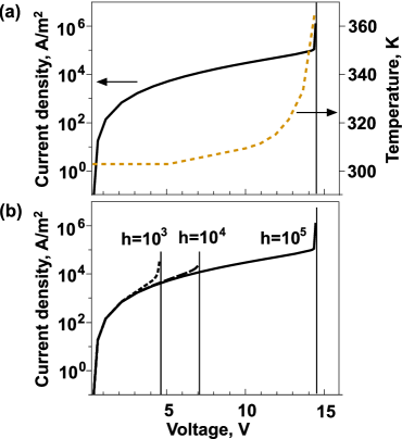
As the voltage is increased, the current and the temperature increase. Remarkably, also the thermal runaway process can be readily identified in this plot as an abrupt end of the recorded current-voltage curve that is preceeded by a sharp kink. The corresponding voltage is indicated by a vertical line in Figure 5-a. Beyond this operating voltage, it is not possible to establish a stable current, because the heat is not sufficiently removed from the device anymore. The better the device is cooled, i.e., the larger the value of , the larger is the critical voltage up to which the OLED operates.
This impact of cooling is illustrated in Figure 5-b, that shows the evolution of the current density - voltage relation for the same charge transport parameters upon increasing the heat transfer coefficient from to . The former value corresponds to the least efficient and the latter value to the most efficient cooling. Again, the operating voltage in which we find the maximum current density and beyond which the current fails to converge is marked with a vertical line. All three current voltage characteristics coincide as long as the OLED is operated safely below 4.5 V. For the least efficient cooling considered, = 103 , the current at 4 V is an order of magnitude larger than the current for a much more efficient cooling ( ). Already small fluctuations in the operating voltage may cause a thermal runaway. The current voltage characteristics do not only reflect the material and geometrical properties of the active layers, but also account for the properties of the exterior layers and, in effect, operating conditions, e.g., whether convective cooling applies.
III.4 Extraction of heat transfer coefficients from experiment
We have developed a rationale (Eq. (8)), according to which the temperature in the electrically active layers is determined by the ratio between the total heat generated per unit area, , and the effective heat transfer coefficients between the electrically active region and the exterior with ambient temperature. With this relation at hand, the question arises whether it is possible to obtain the totally generated heat density directly from experiment to get an estimate for either and for a known device temperature or for known and . Such an estimation is valid as long as the heat transported away from the electrically active region does not influence the temperature inside the this region and preserves a uniform temperature distribution.
The total heat density consists of the Joule heat and the heat due to non-radiative recombination. Knowing the current voltage characteristics, , the Joule heat per unit area , , is readily given by
| (9) |
The recombination heat per unit area , , equals
| (10) |
Therein, the coefficient ensures that exclusively triplet exciton states are considered for the heating and is the recombination energy, measured in electron-volts.
Inserting Eqs. (9,10) into the analytic equation Eq. (7b) for the maximum temperature, we arrive at:
| (11) |
We subjected this relation for to a consistency check to reveal whether we can safely exclude a possible feedback from the heat transported through the encapsulation and substrate layers on the temperature inside the electrically active layers. To this aim, we compared the value extracted from the full simulation with the value obtained from Eq. (11), in which we inserted only the current densities obtained from the simulations. For a realistic thermal conductivity of 0.5 with an voltage of 5 V applied, we calculated from Eq. (11). Eq. (11) reproduces the exact temperature values for a large range of heat transfer coefficients ; for the relative error in predicted temperatures remains below 1 %. Only when approaches values for which the device starts to overheat, either a deviation ( ) or thermal runaways are obtained ( ). Details are shown in the Supporting Information.
IV Conclusions
We investigated how the thermal conductivities of the electrically active organic layers and the heat transfer between the electrically active region and the ambient environment determine the temperature distribution inside OLEDs under operating conditions. To this aim, we established a macroscopic, three-dimensional drift-diffusion based simulation that incorporates charge transport, thermal transport and their mutual coupling for a given OLED stack. In particular, we account for the feedback mechanism of self-heating, that occurs when any dissipation of heat within electrically active layers boosts their electric conductivity which, in turn, enhances the generation of heat. This model allows us to monitor the time-dependent and steady-state behavior of the temperature, the charge carrier densities, the current densities, and local electric fields.
The OLED reaches steady state operation only if the heat is sufficiently well removed from the device to counter-balance self-heating. If either the thermal conductivities or the heat transfer coefficients fall below a certain limit, the blocked outflow of heat promotes a steep increase in the temperature inside the OLED with rising applied voltage. For such a choice of the thermal parameters, any other change in the OLED setup or any fluctuations in operating conditions can trigger the thermal runaway process.
The thermal conductivity of realistically thin organic layers only marginally affect the temperature in the device; in fact, the temperature adopted in an electrically active organic layer is essentially constant. The temperature profile across the entire stack is determined by the thermal properties of the encapsulation layers, the substrate layers, and the heat transfer coefficient associated to heat exchange between the outermost OLED surfaces and the ambient environment. Self-heating arising from an inadequate heat dissipation from the heat source towards the exterior, e.g., due to a limited choice in terms of the substrate, can neither be counter-balanced by a larger thermal conductivity, nor by thicker organic films.
The layers responsible for the major electrical effects differ from the layers in which the relevant thermal effects occur, despite the fact that charge and heat transport strongly couple in the electrically active layers. From a practical point of view that means that the charge transport can be considered and optimized assuming a fixed temperature (e.g., in Kinetic Monte Carlo simulations). The temperature distribution across the entire stack can be, in turn, provided by solving the heat transport equation for the layers outside the electrically active substack.
V Acknowledgement
This work was funded by the Austrian Climate and Energy Fund (KLIEN) and the Austrian Research Promotion Agency (FFG) through the project “ThermOLED” [FFG No. 848905]. The authors would also like to acknowledge the use of HPC resources provided by the ZID of the Graz University of Technology.
References
- Bässler (1993) Bässler, H. (1993), Physica Status Solidi (b) 175 (1), 15.
- Chung et al. (2009) Chung, S., J.-H. Lee, J. Jeong, J.-J. Kim, and Y. Hong (2009), Applied Physics Letters 94 (25), 253302.
- Davids et al. (1997) Davids, P. S., I. H. Campbell, and D. L. Smith (1997), Journal of Applied Physics 82 (12), 6319.
- Davids et al. (1996) Davids, P. S., S. M. Kogan, I. D. Parker, and D. L. Smith (1996), Applied Physics Letters 69 (15), 2270.
- E. Sutherland and R. Hauser (1977) E. Sutherland, J., and J. R. Hauser (1977), IEEE Transactions on Electron Devices ED-24, 363 .
- Fischer et al. (2014) Fischer, A., T. Koprucki, K. Gärtner, M. L. Tietze, J. Brückner, B. Lüssem, K. Leo, A. Glitzky, and R. Scholz (2014), Advanced Functional Materials 24 (22), 3367.
- Fishchuk et al. (2013) Fishchuk, I. I., A. Kadashchuk, S. T. Hoffmann, S. Athanasopoulos, J. Genoe, H. Bässler, and A. Köhler (2013), Physical Review B 88 (12), 125202.
- Fishchuk et al. (2010) Fishchuk, I. I., A. K. Kadashchuk, J. Genoe, M. Ullah, H. Sitter, T. B. Singh, N. S. Sariciftci, and H. Bässler (2010), Phys. Rev. B 81, 045202.
- Gärditz et al. (2007) Gärditz, C., A. Winnacker, F. Schindler, and R. Paetzold (2007), Applied Physics Letters 90 (10), 103506.
- Gruber et al. (2012) Gruber, M., F. Schürrer, and K. Zojer (2012), Organic Electronics 13 (10), 1887 .
- van der Holst et al. (2009) van der Holst, J. J. M., F. W. A. van Oost, R. Coehoorn, and P. A. Bobbert (2009), Phys. Rev. B 80, 235202.
- Jin et al. (2014) Jin, Y., C. Shao, J. Kieffer, M. L. Falk, and M. Shtein (2014), Phys. Rev. B 90, 054306.
- Knapp et al. (2010) Knapp, E., R. Häusermann, H. U. Schwarzenbach, and B. Ruhstaller (2010), Journal of Applied Physics 108 (5), 054504.
- Knapp and Ruhstaller (2011) Knapp, E., and B. Ruhstaller (2011), Optical and Quantum Electronics 42 (11-13), 667.
- Kohári et al. (2013) Kohári, Z., E. Kollár, L. Pohl, and A. Poppe (2013), Microelectronics Journal 44 (11), 1011.
- Langevin (1903) Langevin, M. P. (1903), Ann. Chim. Phys. 28, 433.
- Lee et al. (2014) Lee, J.-H., S. Lee, S.-J. Yoo, K.-H. Kim, and J.-J. Kim (2014), Advanced Functional Materials 24 (29).
- Li et al. (2016) Li, X., X. Yuan, W. Shang, Y. Guan, L. Deng, and S. Chen (2016), Organic Electronics 37, 453 .
- Liemant (1997) Liemant, A. (1997), WIAS Preprint (384), 384.
- Lu et al. (2015) Lu, N., L. Li, and M. Liu (2015), Phys. Rev. B 91, 195205.
- van Mensfoort and Coehoorn (2008) van Mensfoort, S. L. M., and R. Coehoorn (2008), Phys. Rev. B 78, 085207.
- Nenna et al. (2007) Nenna, G., G. Flaminio, T. Fasolino, C. Minarini, R. Miscioscia, D. Palumbo, and M. Pellegrino (2007), Macromolecular Symposia 247 (1), 326.
- Park et al. (2011a) Park, J., H. Ham, and C. Park (2011a), Organic Electronics 12 (2), 227.
- Park and Lee (2014) Park, J. W., and J. H. Lee (2014), Semiconductor Science and Technology 29 (9), 095023.
- Park et al. (2011b) Park, J. W., D. C. Shin, and S. H. Park (2011b), Semiconductor Science and Technology 26 (3), 034002.
- Pasveer et al. (2005) Pasveer, W. F., J. Cottaar, C. Tanase, R. Coehoorn, P. A. Bobbert, P. W. M. Blom, D. M. de Leeuw, and M. A. J. Michels (2005), Phys. Rev. Lett. 94, 206601.
- Reisdorffer, Frederic et al. (2014) Reisdorffer, Frederic,, Garnier, Bertrand, Horny, Nicolas, Renaud, Cedric, Chirtoc, Mihai, and Nguyen, Thien-Phap (2014), EPJ Web of Conferences 79, 02001.
- Ruhstaller et al. (2003) Ruhstaller, B., T. Beierlein, H. Riel, S. Karg, J. C. Scott, and W. Riess (2003), IEEE Journal of Selected Topics in Quantum Electronics 9 (3), 723.
- Scharfetter and Gummel (1969) Scharfetter, D. L., and H. K. Gummel (1969), IEEE Trans. Electron Devices ED-16, 64.
- Scott and Malliaras (1999) Scott, J. C., and G. G. Malliaras (1999), Chemical Physics Letters 299, 115.
- Slawinski et al. (2011) Slawinski, M., D. Bertram, M. Heuken, H. Kalisch, and A. Vescan (2011), Organic Electronics 12 (8), 1399 .
- Triambulo and Park (2016) Triambulo, R. E., and J.-W. Park (2016), Organic Electronics 28, 123 .
- Xu and Xu (2004) Xu, M. S., and J. B. Xu (2004), Journal of Physics D: Applied Physics 37 (12), 1603.
- Zhou et al. (2000) Zhou, X., J. He, L. S. Liao, M. Lu, X. M. Ding, X. Y. Hou, X. M. Zhang, X. Q. He, and S. T. Lee (2000), Advanced Materials 12, 265.