Domain formation and self-sustained oscillations in quantum cascade lasers
Abstract
We study oscillations in quantum cascade lasers due to traveling electric field domains, which are observed both in simulations and experiments. These oscillations occur in a range of negative differential resistance and we clarify the condition determining whether the boundary between domains of different electric field can become stationary.
1 Introduction
Quantum Cascade Lasers (QCLs)FaistScience1994 ; FaistBook2013 have become the most important devices for radiation in the infrared region of the optical spectrum RazeghiApplOpt2017 and are also promising for THz applications RobenOptExpress2017 . They are based on electronic transitions between quantized states in the conduction band of semiconductor heterostructures, which enables a large flexibility to define the transition energy. QCLs are pumped electrically, where a sequence of scattering and tunneling transition fills the upper laser state and empties the lower one. While such an active module has a typical size of 50 nm, the repetition of a large number of modules (the name-giving cascade) allows to fill the optical waveguide with active material. Here the design is based on the assumption, that the applied bias drops homogeneously over all modules. However, tunneling between quantized states is prone to specific resonances CapassoAPL1986 and the appearance of negative differential conductivity (NDC) for fields above the resonance point. In contrast to the resonant-tunneling diode ChangAPL1974 , where this property is directly reproduced in the current-bias relation, the cascaded structure of QCLs provides an instability in the homogeneous voltage drop. This situation is analogous to the well-studied domain formation in Gunn diodes GunnIBM1964 ; KroemerIEEETransElectronDev1966 ; ShawBook1992 and superlattices EsakiPRL1974 ; BonillaPRB1994 ; KastrupAPL1994 ; WackerPhysRep2002 ; BonillaRepProgPhys2005 .
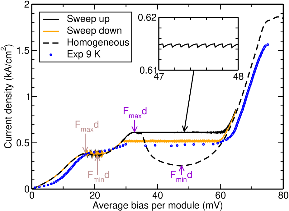
The formation of stationary electrical field domains in QCLs has been observed experimentally by the characteristic saw-tooth structure of the current-bias characteristics LuPRB2006 ; WienoldJAP2011 and a spatially resolved measurement of the bias drop over the sample DharSciRep2014 . Oscillatory behavior has also been reported in the NDC region SirtoriIEEEJQuant2002 which was, however, interpreted to be determined by the circuit similar to resonant tunneling diodes. Specifically, we consider the THz-QCL with scattering injection discussed in DupontJAP2012 . This structure exhibits characteristic regions of NDC in the simulated current density for identical bias drop over all modules (so that periodic boundary conditions apply), as shown in Fig. 1.
Experimentally, current plateaus are observed for biases and currents below threshold. Here we show, both by experiments and simulations, that oscillating electric field domains occur in our device, similar to the case of superlatticesKastrupPRB1995 , and discuss the conditions for their occurrence.
2 Simulating domain formation
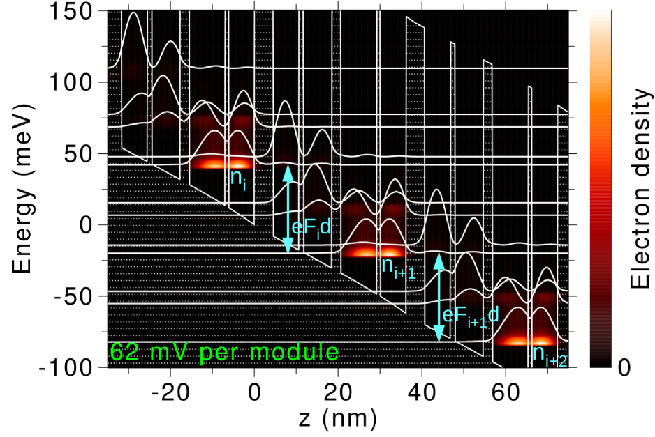
In order to simulate domain formation, we assume that the sheet electron density of each module is essentially confined in a narrow region before the thickest barrier. This is confirmed by our non-equilibrium Green’s function (NEGF) simulations as shown in Fig. 2. (For details, see WingeJAP2016 , where all parameters are givens. As the only difference we use a slightly increased rms height Å for the interface roughness here, which appears to match better with the experimental results. We have no direct experimental information regarding the quality of interfaces.) The same location of charges was actually deduced experimentally DharSciRep2014 . The current to the next module is then essentially determined by the bias drop , where is the average electric field between the electron densities located in module and and nm is the thickness of a single module. Following a common approach in superlattices WackerPhysRep2002 , this current density is approximated by
| (1) |
which assumes that the current density is essentially proportional to the electron density in the injecting module and is reduced by a backward current from thermal excitations in the receiving module . This expression is normalized by the sheet doping density per module, so that the homogeneous current is recovered for . Then the continuity equation provides
| (2) |
where is the number of modules. is the positive elementary charge and we redefine the sign of electric field and current density, so that their signs match the forces and velocity of carriers, respectively. In Eq. (2) we need the boundary currents, which we approximate as
| (3) |
with a phenomenological boundary conductivity , as justified for the Gunn diode in Ref. KroemerIEEETransElectronDev1968 . These Ohmic boundary conditions are common for superlattices, see WackerPhysRep2002 ; BonillaBook2010 for a more detailed discussion. Unless mentioned otherwise, we use , which is steeper than the slopes in . This mimics a good Ohmic contact between the QCL heterostructure and the substrate with an adjacent highly doped () GaAs layer implying a small bias drop . For given electron densities , the electric fields are obtained from the total bias dropping over the QCL
| (4) |
and Poisson’s equation
| (5) |
where is the average relative dielectric constant. For fixed bias , this model has been applied for QCLs in WienoldJAP2011 . Here we consider also the operation by a fixed bias source via a serial load resistance . Following WackerJAP1995 we find
| (6) |
Here is the geometrical capacitance of the QCL structure with and is an additional parallel capacitance, which we actually set to zero here.
The set of equations (1,2,5) can be viewed as the discretization of a drift-diffusion model combined with Poisson’s equation (as appropriate for the Gunn effect KroemerIEEETransElectronDev1966 ). Here, the drift velocity and the diffusion coefficient are given by
respectively, which satisfy the Einstein relation in the linear regime for low fields. This allows for analytic insight into the dynamics of wave-fronts BonillaBook2010 ; BonillaSIAM1997 . However, for many features, such as the existence of stable field domains in a finite range of currents, the discreteness due to the semiconductor heterostructure is essential.
3 Simulation results
Figure 1 shows the simulated current bias relations using a fixed bias . Upon sweeping up the bias, we find two current plateaus; after the first current peak around an average bias of 17 mV per module and also after the second current peak around an average bias of 33 mV per module. The current depends on the sweep direction, a common feature, which has been discussed for superlattices in detail, where multi-stability was observed KastrupAPL1994 . The corresponding distribution of the electric field is shown in Fig. 3. Within the plateau regions, there are two domains with specific electric fields. An increase of bias is reflected in a shift of the domain boundary, where the high-field domain expands.
For the first plateau, the simulations provide actually oscillatory behavior as shown in Fig. 4. These are due to moving domain boundaries (also referred to as fronts), where the excess charge travels along the direction of electron motion. For we obtain an average drift velocity of modules/ns, which is comparable to the average front velocity of 50 modules/ns observed in Fig. 4(a). During the motion of the domain boundary, the electric fields in both domains need to increase in order to maintain the fixed bias. Eventually, the electric field in the low-field domain reaches the NDC region (e.g. at ns) and becomes unstable. Thus, a new accumulation layer is formed within a fraction of a nanosecond, which then starts its motion like the one before. If the sample is operated via a load resistor, the bias is actually oscillating as shown in Fig. 5. In this case the oscillation frequency is reduced.
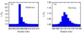
Such oscillations are generic for extended systems with NDC and have been well-studied for the Gunn Diode and superlattices ShawBook1992 ; BonillaBook2010 . In continuous systems, such as the Gunn diode, any charge accumulation typically travels due to the drift velocity (albeit the actual speed may differ KroemerIEEETransElectronDev1966 ) and thus stationary fronts are only possible in the vicinity of the contacts. However, for discrete systems, such as superlattices and QCLs, these fronts can become stationary for a finite range of currents BonillaPRB1994 ; KastrupAPL1994 ; LuPRB2006 ; CarpioPRE2000 , so that the oscillations disappear. Fig. 6 shows the electron density distribution close to the domain boundary in both plateaus. For the first plateau, see Fig. 6(b), the excess electron density , required to change the field between both domains, is spread out over several modules, which resembles the continuous case of the Gunn diode. In contrast, for the second plateau, see Fig. 6(a), a large part of the excess density is essentially located in one module and is trapped by the heterostructure, so that a stationary front appears WackerPRB1997a . This situation should be stable, if the NDC region is crossed within one module. Then at least the part of is located within one module, where denote the position of the current maximum/minimum at the borders of the NDC region, respectively, as indicated in Fig. 1. In order for this to happen, the current in a module with the excess density must match the current of the other modules. Using the approximation for the current (1) under neglect of the backward currents [i.e. the terms with in Eq. (1)], this implies the condition for stationary accumulation fronts
| (7) |
where is the minimum current in the NDC region. A slightly stronger bound has been proven in Eq. (18) of CarpioPRE2000 (also including the backward currents), which justifies the heuristic argument given above. As the low-field domain is only possible for , where is the peak current before the NDC region we find the criterion for stationary domains with accumulation regions
| (8) |
A thorough proof for the stability of stationary domains under this criterion had been provided in WackerPRB1997a without backward current, and follows more generally from CarpioPRE2000 . Based on the homogeneous current-field relations in Fig. 1, we find for the first NDC region, which surpasses the ratio between peak and valley current . This agrees with finding only traveling fronts and oscillatory behavior in this plateau region. For the second plateau is lower than and stationary fronts are possible for currents above according to Eq. (7). This value agrees well with the minimal current density for the domain states upon sweeping down the bias in Fig. 1. In order to compare with experiment, it is important to realize that Eq. (1) is an approximation and that the minimum current density is difficult to access. Furthermore, growth imperfections can shift the range of doping where oscillating field domains are observed in simulations for superlattices WackerPRB1995 . However, the condition (8) should reflect the most important trend, that stationary field domains require large doping densities and a pronounced peak to valley ratio.
4 Experimental results
The experimental data displayed in Fig. 1 show a clear current plateau in the second simulated NDC region (between 34 and 60 mV), while the current is monotonously increasing in the first simulated NDC region around 20 mV. Using a significantly different setup, Ref. DharSciRep2014 reported the occurrence of electric field domains in the second region but a homogeneous bias drop in the first region. This indicates, that the first (weak) NDC region seen in our simulations is not visible in the device. (It also vanishes in the simulations for an increased roughness Å or an elevated temperature of 150 K.) On the other hand, NDC and the formation of electric field domains is manifest in the pronounced second simulated NDC region.
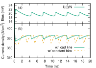
Our measurements are based on 2 s long pulses and the device is operated via a load resistance of 40.7 \textOmega with a similar setup as described in WingePRA2018 . In contrast to WingePRA2018 , the laser bar studied here is indium soldered to a Si carrier with electrodes of negligible resistivity, which simplifies the data analysis. Using a 1 GHz bandwidth oscilloscope, we observe oscillatory behavior in the bias as shown in Figs. 7(a,c). For a heatsink temperature of 80 K, regular oscillations are observed for external bias . From 48.5 V to 49.5 V irregular oscillations are observed, in the sense that the FFT intensity spectrum collapses. While this might indicate some chaotic scenario, we cannot exclude, that these features are triggered by the noise of the input pulses. Above 49.5 V, few sporadic short surges of voltage are still observed indicating some voltage instabilities at the exit of the plateau. At the very beginning of the plateau, from 41.4 to 42.1 V, high amplitude oscillations at fundamental frequency MHz are observed. At 42.1 V, as intense but faster oscillations appear at MHz. As the external bias further increased, the frequency of oscillations increases slightly and its amplitude decreases monotonously. When the regular oscillations vanishes at 48.5 V, the frequency has shifted to MHz. The range of external voltage where the voltage oscillations or instabilities occur is very consistent with the observation of the current plateau. For a heatsink temperature of 9 K, the observed frequencies are lower and the oscillations are not found at all operation points within the plateau.

Concomitant oscillations of the total current (QCL plus voltage probe) measured at the load resistor were also observed and are displayed in Figs. 7(b,d). The current transformer used has a bandwidth of 200 MHz, which limits the resolution here.
5 Simulations with reduced contact conductivity
The experimental observation of oscillations within the second NDC region of Fig. 1 does not agree with the simulated stationary domains discussed in Sec. 3, which are expected due to the stability criterion (8). These stationary field domain distributions show an electron accumulation layer separating the low-field domain close to the injecting contact and the high-field domain at the receiving contact.111Domain distributions with a depletion layer, which have the high-field domain at the injecting contact, are also possible. In order to be stationary, a condition similar to Eq. (8) exists WackerPhysRep2002 , which however requires a substantially higher doping and is not satisfied for our device. Such a field distribution is only possible if the contact field is small at the relevant currents, as otherwise a high-field domain is present at the injecting contact. As discussed in Sec. 3, the stationary domain states require current-densities above as a consequence of the criterion (7). In the following we use a low contact conductivity , which would reflect a significant offset between the elctrochemical potential in the contacting layer and the levels in QCL structures. The chosen value of implies mV for , which is close to at the end of the NDC region. Thus the low-field domain cannot exist at the injecting contact for and the stable domain configurations obtained for the second NDC region in Sec. 3 cannot exist. As a consequence we find oscillatory behavior similar to the experimental observation.
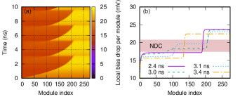
Fig. 8 shows oscillatory behavior for a fixed average bias mV, i.e. in the region of the second plateau. Panel (b) shows a conventional electric field domain distribution at 11 ns. Panel (a) shows that the current density is below and thus the distribution is not stationary but travels to the receiving contact. The constant bias provides a raise in the fields and an increase in current. At 12 ns, the field becomes so large that a high-field domain forms at the injecting contact and starts traveling towards the receiving contact. Simultaneously, the fields drop in all domains and due to the drop of current, the injecting contact can sustain a low-field domain again after 12.5 ns. Afterwards a characteristic period with constant current arises, where the two accumulation fronts travel with half the velocity of the depletion front in between. This scenario is explained in detail for superlattice in Ref. WackerPhysRep2002 . Around 15 ns one accumulation front and subsequently the depletion front vanish at the receiving contact and the cycle is repeated.
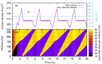
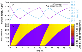
Fig. 9 shows similar domain oscillations under circuit conditions with a load resistor. The frequency is reduced and the signals are altered. Comparing with the electric field distribution in panel (b), we find that the maxima and minima in current from panel (a) are related to the creation of a depletion front at the injection contact and its vanishing at receiving contact, respectively. The corresponding creation and vanishing of the accumulation front is associated with a smaller increase and decrease of slope in the current signal, respectively. The bias behaves precisely the opposite way. Upon varying we find similar results over the entire second NDC region with average current densities around . This current plateau (not shown) agrees excellently with the experimental data in Fig. 1 and the simulated oscillation frequencies are comparable (about a factor two larger) to the experiment (at 80 K). However, the particular shapes of the current and bias signal differ, which might be related to more intricate boundary currents or to details in the circuit such as a parallel capacitance not accounted for in our simulations.
6 Conclusion and discussion
We demonstrated both by simulations and experimentally, that oscillating electric field domains are possible in QCLs. Stationary domains are favored by high doping, a large peak to valley ratio in the NDC region and a small excess charge between the domains as quantified by Eq. (8). Furthermore the injecting contact needs to allow for the presence of a low-field domain at its vicinity for current densities above the minimal current for stationary domain states. can be estimated by Eq. (7). While the simulated current-bias relations agree well with the experimental data, we did not obtain full agreement regarding the details of the oscillations. In particular, the simulations provide domain oscillations in the first NDC region, which appear to be absent in the experiment. This might be related to a higher background current in the experiment, which counteracts the weak NDC feature. Furthermore, the oscillation signals in the second NDC region differ, which we can not explain now. Finally, we want to point out, that very recently some of us observed domain oscillations in a different QCL, which also persisted after the onset of lasing both experimentally and by simulations WingePRA2018 .
7 Acknowledgments
Financial support from the Swedish Science Council (grant 2017-04287) and Nanolund is gratefully acknowledged.
8 Authors contributions
Tim Almqvist did the simulations and Emmanuel Dupont the measurements presented here. The numerical codes were developed by Tim Almqvist, David Winge, and Andreas Wacker, who also guided the work. All the authors were involved in the preparation of the manuscript and approved the final version.
References
- (1) J. Faist, F. Capasso, D.L. Sivco, C. Sirtori, A.L. Hutchinson, A.Y. Cho, Science 264, 553 (1994)
- (2) J. Faist, Quantum Cascade Lasers (Oxford University Press, Oxford, 2013)
- (3) M. Razeghi, W. Zhou, S. Slivken, Q.Y. Lu, D. Wu, R. McClintock, Appl. Opt. 56, H30 (2017)
- (4) B. Röben, X. Lü, M. Hempel, K. Biermann, L. Schrottke, H.T. Grahn, Opt. Express 25, 16282 (2017)
- (5) F. Capasso, K. Mohammed, A.Y. Cho, Appl. Phys. Lett. 48, 478 (1986)
- (6) L.L. Chang, L. Esaki, R. Tsu, Appl. Phys. Lett. 24, 593 (1974)
- (7) J.B. Gunn, IBM J. Res. Dev. 8, 141 (1964)
- (8) H. Kroemer, IEEE Trans. Electron Dev. ED-13, 27 (1966)
- (9) M.P. Shaw, V.V. Mitin, E. Schöll, H.L. Grubin, The Physics of Instabilities in Solid State Electron Devices (Plenum Press, New York, 1992)
- (10) L. Esaki, L.L. Chang, Phys. Rev. Lett. 33, 495 (1974)
- (11) L.L. Bonilla, J. Galán, J.A. Cuesta, F.C. Martínez, J.M. Molera, Phys. Rev. B 50, 8644 (1994)
- (12) J. Kastrup, H.T. Grahn, K. Ploog, F. Prengel, A. Wacker, E. Schöll, Appl. Phys. Lett. 65, 1808 (1994)
- (13) A. Wacker, Phys. Rep. 357, 1 (2002)
- (14) L.L. Bonilla, H.T. Grahn, Rep. Prog. Phys. 68, 577 (2005)
- (15) S.L. Lu, L. Schrottke, S.W. Teitsworth, R. Hey, H.T. Grahn, Phys. Rev. B 73, 033311 (2006)
- (16) M. Wienold, L. Schrottke, M. Giehler, R. Hey, H.T. Grahn, J. Appl. Phys. 109, 073112 (2011)
- (17) R.S. Dhar, S.G. Razavipour, E. Dupont, C. Xu, S. Laframboise, Z. Wasilewski, Q. Hu, D. Ban, Sci. Rep. 4, 7183 (2014)
- (18) C. Sirtori, H. Page, C. Becker, V. Ortiz, IEEE J. Quantum Elect. 38, 547 (2002)
- (19) E. Dupont, S. Fathololoumi, Z.R. Wasilewski, G. Aers, S.R. Laframboise, M. Lindskog, S.G. Razavipour, A. Wacker, D. Ban, H.C. Liu, J. Appl. Phys. 111, 073111 (2012)
- (20) J. Kastrup, R. Klann, H.T. Grahn, K. Ploog, L.L. Bonilla, J. Galán, M. Kindelan, M. Moscoso, R. Merlin, Phys. Rev. B 52, 13761 (1995)
- (21) D.O. Winge, M. Franckié, A. Wacker, Journal of Applied Physics 120, 114302 (2016)
- (22) H. Kroemer, IEEE Transactions on Electron Devices 15, 819 (1968)
- (23) L.L. Bonilla, S.W. Teitsworth, Nonlinear Wave Methods for Charge Transport (Wiley-VCH, Weinheim, 2010)
- (24) A. Wacker, E. Schöll, J. Appl. Phys. 78, 7352 (1995)
- (25) L. Bonilla, SIAM J. Appl. Math. 57, 1588 (1997)
- (26) A. Carpio, L.L. Bonilla, A. Wacker, E. Schöll, Phys. Rev. E 61, 4866 (2000)
- (27) A. Wacker, M. Moscoso, M. Kindelan, L.L. Bonilla, Phys. Rev. B 55, 2466 (1997)
- (28) A. Wacker, G. Schwarz, F. Prengel, E. Schöll, J. Kastrup, H.T. Grahn, Phys. Rev. B 52, 13788 (1995)
- (29) D.O. Winge, E. Dupont, A. Wacker, Phys. Rev. A 98, 023834 (2018)