Efficient Wave Optics Modeling of
Nanowire Solar Cells Using
Rigorous Coupled Wave Analysis
Abstract
We investigate the accuracy of rigorous coupled wave analysis (RCWA) for near-field computations within cylindrical GaAs nanowire solar cells and discover excellent accuracy with low computational cost at long incident wavelengths, but poor accuracy at short incident wavelengths. These near fields give the carrier generation rate, and their accurate determination is essential for device modeling. We implement two techniques for increasing the accuracy of the near fields generated by RCWA, and give some guidance on parameters required for convergence along with an estimate of their associated computation times. The first improvement removes Gibbs phenomenon artifacts from the RCWA fields, and the second uses the extremely well-converged far field absorption to rescale the local fields. These improvements allow a computational speedup between 30 and 1000 times for spectrally integrated calculations, depending on the density of the near fields desired. Some spectrally resolved quantities, especially at short wavelengths, remain expensive, but RCWA is still an excellent method for performing those calculations. These improvements open up the possibility of using RCWA for low cost optical modeling in a full optoelectronic device model of nanowire solar cells.
References
- [1] D. Wu, X. Tang, K. Wang, and X. Li, “An Analytic Approach for Optimal Geometrical Design of GaAs Nanowires for Maximal Light Harvesting in Photovoltaic Cells,” \JournalTitleScientific Reports 7, 46504 (2017).
- [2] B. C. P. Sturmberg, K. B. Dossou, L. C. Botten, A. A. Asatryan, C. G. Poulton, R. C. McPhedran, and C. M. de Sterke, “Optimizing Photovoltaic Charge Generation of Nanowire Arrays: A Simple Semi-Analytic Approach,” \JournalTitleACS Photonics 1, 683–689 (2014).
- [3] J. Wallentin, N. Anttu, D. Asoli, M. Huffman, I. Aberg, M. H. Magnusson, G. Siefer, P. Fuss-Kailuweit, F. Dimroth, B. Witzigmann, H. Q. Xu, L. Samuelson, K. Deppert, and M. T. Borgström, “InP Nanowire Array Solar Cells Achieving 13.8% Efficiency by Exceeding the Ray Optics Limit,” \JournalTitleScience 339, 1057–1060 (2013).
- [4] J. Kupec, R. L. Stoop, and B. Witzigmann, “Light absorption and emission in nanowire array solar cells,” \JournalTitleOptics Express 18, 27589–27605 (2010).
- [5] O. M. Ghahfarokhi, N. Anttu, L. Samuelson, and I. Åberg, “Performance of GaAs Nanowire Array Solar Cells for Varying Incidence Angles,” \JournalTitleIEEE Journal of Photovoltaics 6, 1502–1508 (2016).
- [6] K. L. Kavanagh, “Misfit dislocations in nanowire heterostructures,” \JournalTitleSemiconductor Science and Technology 25, 024006 (2010).
- [7] M. T. Borgström, M. H. Magnusson, F. Dimroth, G. Siefer, O. Höhn, H. Riel, H. Schmid, S. Wirths, M. Björk, I. Åberg, W. Peijnenburg, M. Vijver, M. Tchernycheva, V. Piazza, and L. Samuelson, “Towards Nanowire Tandem Junction Solar Cells on Silicon,” \JournalTitleIEEE Journal of Photovoltaics 8, 733–740 (2018).
- [8] K. W. Robertson, R. R. LaPierre, and J. J. Krich, “Optical Optimization of Passivated GaAs Nanowire Solar Cells,” in Proc. IEEE 44th Photovoltaic Spec. Conf., (Washington, D.C, 2017), p. 5.
- [9] Y. Hu, R. R. LaPierre, M. Li, K. Chen, and J.-J. He, “Optical characteristics of GaAs nanowire solar cells,” \JournalTitleJournal of Applied Physics 112, 104311 (2012).
- [10] K. M. Azizur-Rahman and R. R. LaPierre, “Wavelength-selective absorptance in GaAs, InP and InAs nanowire arrays,” \JournalTitleNanotechnology 26, 295202 (2015).
- [11] A. H. Trojnar, C. E. Valdivia, R. R. LaPierre, K. Hinzer, and J. J. Krich, “Optimizations of GaAs Nanowire Solar Cells,” \JournalTitleIEEE Journal of Photovoltaics 6, 1494–1501 (2016).
- [12] K. T. Fountaine, W. S. Whitney, and H. A. Atwater, “Resonant absorption in semiconductor nanowires and nanowire arrays: Relating leaky waveguide modes to Bloch photonic crystal modes,” \JournalTitleJournal of Applied Physics 116, 153106 (2014).
- [13] Q. G. Du, C. H. Kam, H. V. Demir, H. Y. Yu, and X. W. Sun, “Broadband absorption enhancement in randomly positioned silicon nanowire arrays for solar cell applications,” \JournalTitleOptics Letters 36, 1884–1886 (2011).
- [14] M. G. Moharam, T. K. Gaylord, E. B. Grann, and D. A. Pommet, “Formulation for stable and efficient implementation of the rigorous coupled-wave analysis of binary gratings,” \JournalTitleJOSA A 12, 1068–1076 (1995).
- [15] M. Weismann, D. F. Gallagher, and N. C. Panoiu, “Accurate near-field calculation in the rigorous coupled-wave analysis method,” \JournalTitleJournal of Optics 17, 125612 (2015).
- [16] P. Lalanne and M. P. Jurek, “Computation of the near-field pattern with the coupled-wave method for transverse magnetic polarization,” \JournalTitleJournal of Modern Optics 45, 1357–1374 (1998).
- [17] K.-H. Brenner, “Aspects for calculating local absorption with the rigorous coupled-wave method,” \JournalTitleOptics Express 18, 10369–10376 (2010).
- [18] E. A. Bezus and L. L. Doskolovich, “Stable algorithm for the computation of the electromagnetic field distribution of eigenmodes of periodic diffraction structures,” \JournalTitleJOSA A 29, 2307–2313 (2012).
- [19] V. Liu and S. Fan, “S4 : A free electromagnetic solver for layered periodic structures,” \JournalTitleComputer Physics Communications 183, 2233–2244 (2012).
- [20] L. Li, “Formulation and comparison of two recursive matrix algorithms for modeling layered diffraction gratings,” \JournalTitleJournal of the Optical Society of America A 13, 1024 (1996).
- [21] D. M. Whittaker and I. S. Culshaw, “Scattering-matrix treatment of patterned multilayer photonic structures,” \JournalTitlePhysical Review B 60, 2610–2618 (1999).
- [22] M. G. Moharam and A. B. Greenwell, “Rigorous analysis of field distribution and power flow in grating coupler of finite length,” in Diffractive Optics and Micro-Optics, (Optical Society of America, 2004), p. DMC5.
- [23] H. Kim, I.-M. Lee, and B. Lee, “Extended scattering-matrix method for efficient full parallel implementation of rigorous coupled-wave analysis,” \JournalTitleJournal of the Optical Society of America A 24, 2313 (2007).
- [24] R. C. Rumpf, “Improved formulation of scattering matrices for semi-analytical methods that is consistent with convention,” \JournalTitleProgress In Electromagnetics Research B 35, 241–261 (2011).
- [25] S. Adachi, Optical Constants of Crystalline and Amorphous Semiconductors: Numerical Data and Graphical Information (Springer US, 1999), 1st ed.
- [26] P. Götz, T. Schuster, K. Frenner, S. Rafler, and W. Osten, “Normal vector method for the RCWA with automated vector field generation,” \JournalTitleOptics express 16, 17295–17301 (2008).
- [27] L. Li, “Use of Fourier series in the analysis of discontinuous periodic structures,” \JournalTitleJOSA A 13, 1870–1876 (1996).
- [28] “Standard Tables for Reference Solar Spectral Irradiances: Direct Normal and Hemispherical on 37° Tilted Surface,” Tech. rep., ASTM International (2012).
- [29] O. Tange, GNU Parallel 2018 (Ole Tange, 2018).
1 Introduction
Nanowire solar cells (NWSC) are a new solar cell technology with the potential to improve upon existing solar cell devices. Their potential stems from their ability to effectively absorb incident light while using less semiconductor material than planar solar cells.
The optimal nanowire solar cell arrays consists of nanowires that are a few microns in height and with diameters and periodicities comparable to the wavelengths present in the solar spectrum [1, 2]. These small sizes require full wave optics simulations to accurately model their optical properties, unlike in standard planar devices [3, 4]. Both experimental measurements and modeling have shown high levels of absorption with low sensitivity to the incident angle of light [5]. Additionally, the finite in-plane dimensions of nanowires can accommodate strain due to growth on lattice-mismatched substrates without introducing dislocation faults in the crystal lattice [6]. This capability opens up the possibility for III-V tandem cells grown on silicon [7].
The larger design parameter space of NWSC relative to planar solar cells requires careful optimization of geometric parameters to maximize device performance [8]. There is a need for fast, accurate modeling tools to enable rapid exploration and optimization of nanowire designs. Conventionally, finite element [9, 4, 10, 11] and finite difference methods [1, 12, 13] have been used in optical models of NWSC. While these techniques are highly accurate, they are computationally expensive, limiting their usefulness in a closed-loop global device optimization. Rigorous coupled wave analysis (RCWA) is another wave-optics modeling technique that lacks the memory and computational requirements of competing techniques [14]. RCWA is a Fourier domain technique ideally suited to periodic arrays. It is promising for its speed and is highly accurate when computing far-field quantities such as total absorptance, reflectance, and transmittance. RCWA simulations become more accurate as the number of plane waves increases, and the computational cost scales as . However, naive implementations lack accuracy at reasonable when computing near-fields internal to the device due to the well-known Gibbs phenomenon [15]. Such near-fields are required to compute carrier generation rates and are thus an essential component of a fully-coupled optoelectronic device model.
In this work, we assess the accuracy of RCWA for use in optical modeling of nanowire solar cells. We examine a test device (see Fig. 1 and Table 1), indicate where RCWA lacks a desirable level of accuracy, and provide two techniques for increasing accuracy of the near fields. The first is an implementation of an already published technique for introducing proper discontinuities in the near fields and mitigating the Gibbs phenomenon [16, 17, 15, 18]. The second is a new rescaling technique that increases the accuracy of device simulations while keeping computational cost reasonable when computing spectrally integrated quantities. We show that even with our two improvements, some spectrally resolved quantities continue to require more expensive calculations. Using our improvements, RCWA shows promise as an effective technique for rapid optical modeling of nanowire solar cells.
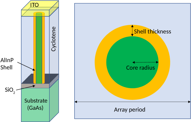
| Parameter | Value |
|---|---|
| NW Core Length | 1.3 |
| NW Shell Length | 1.27 |
| SiO2 Thickness | 30 nm |
| Substrate Thickness | 1 |
| ITO Thickness | 300 nm |
| Array Period | 250 nm |
| Core Radius | 60 nm |
| Shell Thickness | 20 nm |
2 RCWA
RCWA is a Fourier-space method for solving the source-free frequency domain Maxwell’s equations:
| (1) | ||||
| (2) | ||||
| (3) | ||||
| (4) |
where is the magnetic field, is the electric field, is the oscillation frequency, is the electric permitivitty, and is the magnetic permeability. RCWA relies on two critical assumptions about the geometry of the system. First, the device must be composed of discrete, axially-invariant layers such that at a given - point within a layer, the material parameters along the z-direction remain constant. Second, the device must be decomposable into fundamental unit cells that are 2D periodic in the plane. If these conditions are satisfied, then the longitudinal and transverse dimensions are separable and the fields in a single layer can be written as:
| (5) |
where is one of in-plane reciprocal lattice vectors, is the in-plane component of the excitation, and . Note the is generally chosen to be an array of reciprocal lattice points with a circular truncation, keeping all with less than some constant, which maintains symmetry in Fourier space [19]. The in-plane dielectric profile may depend on the material, allowing it to have piecewise-constant dependence on the transverse spatial coordinates. Vertical nanowire arrays (see Fig. 1) satisfy these geometric constraints.
The essential part of RCWA is determining in Eq. (5) for a given set of reciprocal lattice vectors . One can assume the coefficients in Eq. (5) take the form [19]
| (6) |
where the are expansion coefficients and the z-component has been chosen to satisfy the condition. This form of the fields illustrates one of the key advantages of RCWA over competing techniques, namely the analytic dependence on the z coordinate. By inserting Eq. (6) into Eq. (1), one arrives at an eigenvalue equation for determining the set of eigenvalues and the components of the eigenvectors for a single layer. Once the eigenmodes of each layer have been determined, multilayer structures are joined together by introducing propagation amplitudes for the eigenmodes and using the scattering matrix method to join solutions at layer interfaces [20, 21, 22, 23, 24]. Results increase in accuracy with . Our work is an extension to S4, an open-source implementation of RCWA built on the scattering matrix method [19]. In the remainder of the manuscript, we refer to S4 as the standard RCWA method, but it has included a significant number of improvements from the original RCWA methods; for details, see Ref. 19.
For optoelectronic device modeling, we are most concerned with determining the local carrier generation rate, which is determined from the local electric field strength in each material. RCWA expresses the fields using the Fourier series in Eq. (5). Any finite Fourier series representation is always continuous, even across in-plane material interfaces, as between the core and shell of a nanowire. In an exact solution, the normal components of should be discontinuous across material boundaries, but a Fourier reconstruction requires an intractable number of terms to accurately model such a discontinuity, even though far-field quantities such as the total absorptance may be well converged. For any finite , standard RCWA-produced fields have spurious oscillations, especially near material interfaces.
To assess the convergence of RCWA with , we define two methods for computing the absorptance of a layer of the device. The first method relies only on the power exiting from the top of the layer and the power transmitting through the bottom of the layer. These powers can be computed entirely in Fourier space [19], and do not suffer from convergence issues in the reconstruction of the near fields. These emitted powers of layer are defined as:
| (7) | ||||
| (8) |
where is the z-component of the Poynting vector and the integration is over the top or bottom surface of the unit cell, with the appropriate sign for emitted power. Considering the top (layer 1) and bottom (layer ) together, the total reflectance and transmittance are
| (9) | ||||
| (10) |
where is the input power of the incident plane wave. Then total absorptance is:
| (11) |
The contribution of a single layer to the device absorptance can be calculated similarly. We consider the test structure detailed in Table 1 and use S4 [19] to perform RCWA calculations with normally-incident circularly polarized light. We consider 60 equally spaced frequencies corresponding to wavelengths from 300 nm to 900 nm, just beyond the GaAs absorption edge of 871 nm.
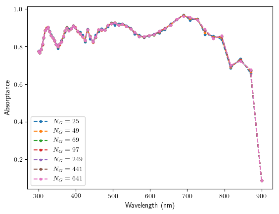
Figure 2 shows that the far-field absorptance spectrum of the full device converges rapidly with basis terms, and is self-converged within 0.5% with .
Equation (11) expresses the power absorbed in a layer in terms of the fluxes into and out of the layer. The divergence theorem and Maxwell’s equations allow rewriting that power in terms of the local fields, instead. The absorbed power can then be written,
| (12) | ||||
| (13) |
The complex dielectric at each frequency is constructed from tabulated real and imaginary parts of the index of refraction in each material [25, 9].
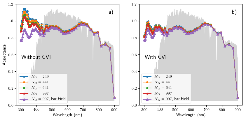
We calculate by extracting on a cubic mesh with 1 nm spacing in the plane for all layers. We use 3 nm spacing along the z-direction in the ITO layer and 3.5 nm spacing in the nanowire layer. A sparser mesh of 16 nm spacing is used in the substrate due to the weak absorption there. This choice of mesh is sufficiently dense to converge the result better than 1% using a simple trapezoidal rule integration. Figure 3a shows the convergence of with . Though the near fields are well converged for nm, they are not converged at short wavelengths even for .
In the following sections, we provide two techniques for improving the accuracy of the near fields in RCWA. The first is an implementation of an existing technique, which we call the continuous variable formulation (CVF), which mitigates the Gibbs phenomenon and ensures proper discontinuities at interfaces by modifying the field computations such that only quantities that are continuous in real space are reconstructed from their Fourier components. The discontinuities across in-plane material boundaries are then handled in real space. The second technique uses the well-converged, highly accurate far-field computation of each layer’s absorption to rescale the near fields, ensuring correct total generation within a device layer.
3 Continuous Variable Formulation
The CVF is a modification to RCWA that only Fourier reconstructs quantities which are continuous across material interfaces in real space. These quantities are the components of the displacement field that are normal to, and the components of the electric field that are tangential to, a material interface. Using these real-space continuous quantities, one can determine the full electric field everywhere by using the constitutive relationship
| (14) |
with a discontinuous real-space . S4 already uses a related technique for calculating the Fourier modes, but it does not use this method when extracting real-space quantities.
To compute the normal and tangential components of any electromagnetic (EM) field, one must construct a locally-defined vector field that is both tangent to all material interfaces in the unit cell and periodic in the in-plane coordinates, which can be generated automatically, as is done by S4 [26, 19]. This vector field induces an associated projection operator that can be used to project the Cartesian components of the EM fields onto this local coordinate system such that:
| (15) | ||||
| (16) |
where , is the component of along the tangential vector field and is the component of perpendicular to the tangential vector field. The total field satisfies
| (17) |
By taking the Fourier transform of , the projection onto the tangential vector field can also be done in Fourier space. Mirroring the notation of Ref. 15, we denote discrete real-space quantities with upper case letters (as in to represent the vector for many points ), vectors of Fourier coefficients with lower case letters surrounded by single brackets (as in ), and Fourier space matrix operators with double brackets (as in ). Using this notation, the Fourier transform of Eq. 15 is given by [15]:
| (18) |
where is the Fourier convolution matrix [19, 15]. That is, one calculates the Fourier transform of , and the (, ) element of is .
We extract and from a standard RCWA implementation and then construct and . Since and are both discontinuous, the proper Fourier factorization takes [27]
| (19) |
where is the block diagonal matrix whose upper-left and lower-right blocks are the inverse of the Fourier convolution matrix of . Reference 15 showed that the symmetric formulation,
| (20) |
converges well and conserves power for lossless structures.
After finding and we reconstruct the real space electric field
| (21) |
where indicates the inverse Fourier transform. This has correct discontinuities at material interfaces where jumps. Finally, the real space electric fields in Cartesian coordinates can be recovered using:
| (22) | ||||
| (23) |
Figure 4 shows the norm-squared components of the electric fields computed using unmodified RCWA and the CVF on a line cut along the x-direction through the center of the nanowire. In this cut, is normal to the interface and should therefore be discontinuous, while should be continuous. Note the Gibbs oscillations in the standard result for , while the CVF result has introduced discontinuities at the boundaries and significantly reduced the amplitude of the Gibbs oscillations.
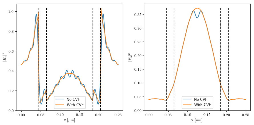
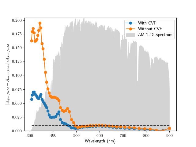
Figure 3b shows the improved agreement between the CVF absorptance and the well converged far field absorptance. Figure 5 shows the relative difference between the far and near field absorptances calculated with and without the CVF. It is clear that the CVF significantly improves the agreement at all wavelengths, but the disagreement is still significant for wavelengths shorter than 450 nm. Figure 5 indicates the AM1.5G spectrum, which shows that the CVF-based agrees well with the far field results through the most important parts of the solar spectrum. In the next section, we introduce a simple rescaling technique to increase accuracy of the near fields at all incident wavelengths.
4 Rescaling Technique
In device simulations, the total optical generation rate must be determined accurately. The exact position where generation occurs is somewhat less important, as the carriers drift and diffuse, and deviations on the scale of a few nanometers are rarely significant. We can ensure that the total generation in each layer is calculated correctly, even with inexpensive RCWA calculations that have not fully converged the local fields. To achieve this goal, we use the well-converged far field results (as shown in Fig. 2) to rescale the components of the near fields in each layer such that and agree exactly. This rescaling can be done by defining a rescaling factor for each layer and frequency :
| (24) |
Then, the components of may be rescaled such that:
| (25) |
for fields in the appropriate layer.
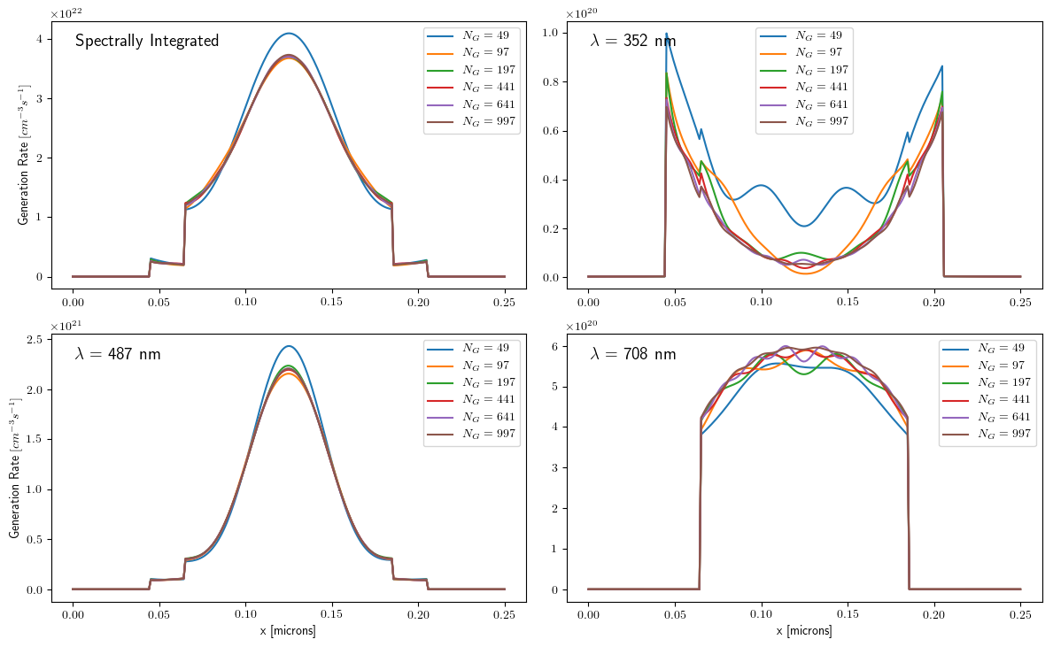
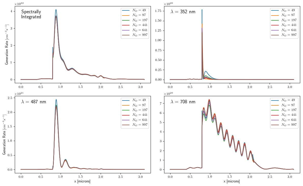
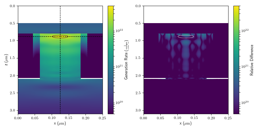
This rescaling technique allows accurate determination of spectrally-integrated generation rates with small numbers of basis terms. Figures 6 and 7 show line cuts through the test structure at three representative wavelengths and spectrally integrated under AM1.5G illumination [28], calculated with 60 equally spaced frequencies. At 487 nm, the fields are quantitatively converged at small , while the Gibbs oscillations are not entirely removed either at shorter or longer wavelengths. Calculations dependent on spectrally resolved local fields, such as external quantum efficiency (EQE), thus require relatively large at some wavelengths. When the fields are spectrally integrated, however, the essentially random phases of the oscillations average away, and the spectrally-integrated fields are quantitatively converged by . Figure 8 compares the rescaled spectrally-integrated generation rates along a plane through the center of the nanowire at and 197, showing the excellent agreement that rescaling permits, even at low . This spectrally integrated generation rate is sufficient for optoelectronic modeling while reducing the requirements for by a factor of 5.
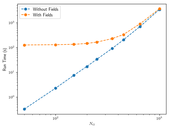
The computational cost of the RCWA method scales as , so reducing by a factor of 5 (from 1000 to 200) theoretically reduces the runtime by a factor of 125, and reducing to can reduce the runtime by a factor of 1000. Extracting the electric fields on a dense mesh of points, however, also has a computational cost, and for sufficiently small , this electric-field extraction limits the runtime. Figure 9 shows an estimate of the simulation run times for a single incident wavelength. Each desired wavelength must be calculated separately, and they all take approximately the same amount of processor time. Simulations were run on a single core of an Intel Xeon E5-2640 v4 CPU with a 2.40GHz clock speed. The figure shows both the simulation time for RCWA to determine the field amplitudes, in Fourier space, and for the extraction of those fields on the dense real-space mesh described above. The CVF method does not significantly change the run times. Efforts were made to minimize data input/output time and resource contention in all benchmarks. These results show that running at has a cost 25 times less than at , and that cost is dominated by the field calculation and export. The field calculation and export time can possibly be optimized further and would certainly be reduced if a coarser mesh were requested. Decreasing that cost could allow computation times to be reduced by an additional factor of 5. Simulations at each frequency are completely independent, so computation time for a full spectral sweep can be easily reduced by running all frequencies in parallel [29]. With a sufficient number of CPU cores, a full spectral sweep can be run in the same clock time as a single simulation.
5 Conclusion
In this work, we investigate the accuracy of RCWA for optical modeling of nanowire solar cells. We find excellent accuracy with low computational cost at long incident wavelengths, but poor accuracy at short incident wavelengths. To increase the accuracy of RCWA we extend the open-source library S4 [19] to include an already published technique for improving near field computations in RCWA [15]. Our implementation mitigates the Gibbs phenomenon and introduces physically expected discontinuities in the fields at material interfaces, improving convergence of the near fields at all incident wavelengths. To bring convergence within a 1% tolerance, we introduce a simple rescaling technique that uses the well converged far field quantities to rescale the near fields on a per layer basis. These improvements open up the possibility of using RCWA as a low cost optical modeling technique in a full optoelectronic device model of nanowire solar cells.
6 Acknowledgements
We thank Anna Trojnar for helpful conversations and acknowledge funding from the Natural Sciences and Engineering Research Council of Canada.