Magnetic field sensing with the kinetic inductance of a high- superconductor
Abstract
We carry out an experimental feasibility study of a magnetic field sensor based on the kinetic inductance of the high- superconductor yttrium barium copper oxide. We pattern thin superconducting films into radio-frequency resonators that feature a magnetic field pick-up loop. At 77 K and for film thicknesses down to 75 nm, we observe the persistence of screening currents that modulate the loop kinetic inductance. According to the experimental results the device concept appears attractive for sensing applications in ambient magnetic field environments. We report on a device with a magnetic field sensitivity of pT, an instantaneous dynamic range of T, and operability in magnetic fields up to T.
The kinetic inductance of superconductors has found many applications in fields as diverse as bolometry Timofeev et al. (2017); Lindeman et al. (2014), parametric amplification Ho Eom et al. (2012); Ranzani et al. (2018), current detectors Wang et al. (2018), and sensing of electromagnetic radiation Rantwijk et al. (2016); Sato et al. (2018), to name but a few. Each device harnesses a certain type of a non-linearity of the kinetic inductance , such as that induced by temperature, electric current, or non-equilibrium quasiparticles. In sensor applications, radio-frequency (rf) techniques are often employed in observation of the variations of : a high sensitivity follows from the intrinsically low dissipation of the superconductors, manifesting itself as a high quality factor of resonator circuits, for example.
The general advantages common to all sensors have motivated the development of kinetic inductance magnetometers (KIMs), devices that combine the current non-linearity with magnetic flux quantization Luomahaara et al. (2014); Asfaw et al. (2018). In comparison to the most established category of sensitive magnetometers, i.e., superconducting quantum interference devices (SQUIDs), KIMs have certain benefits. KIM fabrication involves only a single-layer process that avoids Josephson junctions which are the central components of SQUIDs. Furthermore, KIMs typically have a higher dynamic range, and they enable operation in demanding ambient magnetic field conditions. KIMs also unlock the ability to use frequency multiplexing for the readout of large sensor arrays where each magnetometer has a dedicated eigenfrequency Rantwijk et al. (2016); Sipola et al. (2018).
In this Letter, we demonstrate KIMs fabricated from yttrium barium copper oxide (YBCO). YBCO is a high- superconductor that enables KIM operability at elevated temperatures , allowing for cooling with liquid nitrogen. Non-linear of YBCO has previously been evaluated for bolometric Lindeman et al. (2014) (direct Sato et al. (2018)) detection of infrared (optical) radiation. A further benefit of the material is its high tolerance against background magnetic fields, which has recently culminated in a YBCO rf resonator with a quality factor of about at K and at a magnetic flux density of T applied parallel to the superconducting film Ghirri et al. (2015). From a sensitivity viewpoint, an important benchmark for our KIM are state-of-the-art YBCO SQUID magnetometers Faley et al. (2017) that have a sensitivity better than . However, these SQUIDs suffer from a complicated fabrication process that makes mass production difficult, and in order to extend the dynamic range beyond a few nT, they need to be operated in a flux-locked loop requiring at least four wires to each cold sensor.
We review the KIM operating principle, starting from the current non-linearity Zmuidzinas (2012); Vissers et al. (2015),
| (1) |
In anticipation of using it for magnetometry, we have plugged in a screening current , the flow of which is enforced by magnetic flux quantization. is the kinetic inductance at , and is a normalizing current on the order of the critical current . Assuming that is a property of a superconducting loop with an area , we formulate the flux quantization as
| (2) |
where is loop geometric inductance, the spatial average of the magnetic flux density threading the loop, and an integer times the magnetic flux quantum. Sensitive magnetometry calls for a decent kinetic inductance fraction , and an effective method of observing the -induced inductance variations. To establish an rf readout, two opposite edges of the loop are connected with a capacitor that leaves unperturbed, but creates an rf eigenmode together with the loop inductance. Then, the inductance variation translates into a changing resonance frequency, a quantity which is probed by coupling the resonator weakly into a 50- readout feedline. Two KIMs of this kind have recently been reported: the materials of choice have been NbN Luomahaara et al. (2014) and NbTiN Asfaw et al. (2018), both of which are low- superconductors whose disordered nature provides a magnetic penetration depth Vissers et al. (2010) exceeding several hundreds of nm. For films with a thickness , the kinetic surface inductance equals , with the vacuum permeability.
In the design of our high- KIM [Fig. 1(a)], we use as a guideline the theoretical responsivity on resonance Luomahaara et al. (2014)
| (3) |
that describes how the magnetic flux sensitivity of the resonator voltage is related to the electrical and geometric device parameters. The readout rf power is expressed through an excitation voltage amplitude . The total inductance equals one quarter of the loop inductance plus the contribution of the parasitic trace connecting the two halves of the loop. () denotes the loaded (external) quality factor. We choose a maximal loop area allowed by fabrication technology . We anticipate that reaching a significant is the main bottleneck: The reported values Ghigo et al. (2004) of the YBCO in the low- limit are only nm, and few devices have previously featured long superconducting traces with a small cross-section Hattori, Yoshitake, and Tahara (1998). We select a conservative value of m, and compare devices with a variable nm. The shunt capacitor pF, which determines the unloaded angular resonance frequency through the relation , is formed from interdigitated fingers of width m and gap m. We target a loaded resonance frequency of about MHz.
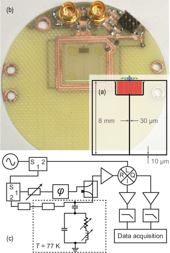
Sample A was fabricated on a r-cut sapphire substrate with a yttria-stabilized zirconia (YSZ) and a CeO2 buffer layer to support the epitaxial growth of a nm YBCO film. As the deposition process of thin YBCO films is optimized for MgO, Sample B (Sample C) with a nm ( nm) YBCO film was fabricated on a 110 MgO substrate without buffer layers instead. Low-loss microwave-resonant YBCO structures have previously been reported on both substrate materials Ghirri et al. (2015); Sato et al. (2018). The YBCO films were deposited with pulsed laser deposition (PLD) and the devices were then patterned with optical lithography using a laser writer and argon ion beam etching. For Samples A and C a simple S1318 photoresist mask was used, while for Sample B a hard carbon mask was chosen to avoid degradation of the thin superconducting film by the photoresist. The carbon mask was deposited with PLD and patterned by oxygen plasma etching through a Cr mask. The ion beam etching process was monitored with secondary ion mass spectrometry for endpoint detection. We attach the KIMs onto a printed circuit board (PCB) that has copper patterns for rf wiring and magnetic bias coils [Fig. 1(b)].
The first KIM characterization is the measurement of the resonance lineshape and its sensitivity to the magnetic field. As makes the resonator a sensitive thermometer Lindeman et al. (2014), we resort to immersion cooling in liquid nitrogen at K. We use a high-permeability magnetic shield that not only protects the sample from magnetic field noise, but also prevents trapping of flux vortices during the time when the sample crosses . The core elements of the readout electronics are a low-noise rf preamplifier noa followed by a demodulation circuit (IQ mixer), and analog-to-digital converters [Fig. 1(c)]. We sweep the frequency of a weak ( -66 dBm) rf tone across the resonance. We simultaneously apply a static as well as a weak ac probe tone at a frequency of 1 kHz. From the averaged in-phase (I) and quadrature (Q) components of the output we extract the complex-valued transmission parameter . In addition, we use ensemble averaging of the modulated output voltage to extract the responsivity corresponding to the probe tone.
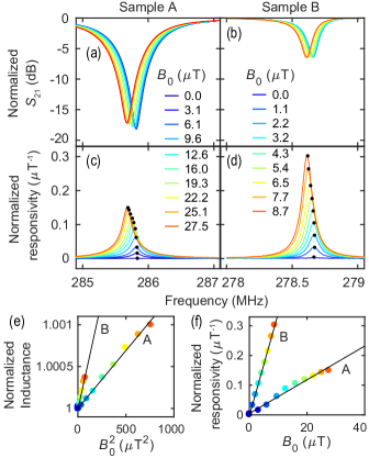
From the best fits Megrant et al. (2012) to we extract , , and the internal quality factor . Applying shifts downwards in Samples A and B [Fig. 2(a,b)], but not in Sample C which has the thinnest film. We suspect that a residual dc resistance prohibits the proper flux quantization. However, also Sample C reacts to an ac magnetic excitation, and at a lower K we observe the proper dc response as well. We convert the frequency shifts of Samples A and B into an equivalent change in and observe a quadratic dependence on [Fig. 2(e)], which is in line with Eqs. (1-2). Unlike in low- KIMs Luomahaara et al. (2014); Asfaw et al. (2018), we do not observe reseting of the sample to [i.e., into a finite in Eq. (2)] upon crossing a threshold corresponding to . Instead, the resonance of Sample A (B) stays put at (). We attribute this to flux trapping that most likely occurs at the sample corners where the inhomogeneous bias field of the square coil is the strongest (about ). Ref. Sun, Gallagher, and Koch, 1994 proposes a flux-trapping condition of the form where is the critical current density.
Regarding the quality factors, we note that Sample A is overcoupled with much smaller than . Sample B is close to being critically coupled (, ). The observed variations are on the order of . Low internal dissipation is key to achieving high device sensitivity. Thus, we discuss the possible mechanisms affecting . Firstly, the resistive part of the superconductor rf surface impedance generates loss that grows with increasing , , and surface roughness Zaitsev et al. (2002); Wang et al. (2003). The dielectric losses of the substrates should not play a role: both sapphire and MgO have low relative permittivity (sapphire: and anisotropic, MgO: ) and low dielectric loss tangents Krupka et al. (1994); Buckley, Agnew, and Pells (1994); Taber and Flory (1995) (<) at K. A loss mechanism related to the PCB deserves further attention: the presence of the bias coils made of resistive copper. In Ref Luomahaara et al., 2014 as well as for the data presented in Figs. 2-3 for Sample A, bias coil rf decoupling is attemped with series impedances (resistance, inductance) on the order of hundreds of Ohms within the coils. This has allowed for , but we have learned that higher values can be reached with an arrangement where the bias coils are grounded at rf and the readout is mediated by stray coupling between the KIM and the coils noa . Samples B and C as well as a subsequent cooldown of Sample A (Fig. 4) have been prepared using this new method.
The device responsivities are presented in Fig. 2(c,d) as a function of the readout frequency. They are of the normalized form : this is a convenient quantity because both and V experience the same gain of the readout electronics. The measured readout frequency dependencies are Lorentzians that peak on resonance. We use these data for the estimation of the sensor dynamic range Luomahaara et al. (2014), which is approximately T (T) for Sample A (B) at high responsivity. As expected, the responsivity vanishes at the first-order flux-insensitive points where . The peaks of the responsivity Lorentzians, shown as a collection in Fig. 2(f), are linearly proportional to . If we normalize Eq. (3) in the limit of low ,
| (4) |
we obtain a model which is in line with the measured trend since there is an approximately linear mapping from into [consider Eq. (1) at ]. The measured linear slope of the responsivity is about six times steeper in Sample B, which is primarily an indication of a higher and a lower resulting from the thinner film.
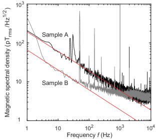
To determine the magnetic field sensitivity of Samples A and B, we record s voltage traces and average the squared modulus of their Fourier transform. We do this at as a function of : importantly, a carrier cancellation circuit [Fig. 1(c)] is activated now to avoid the saturation of the electronics. We also compare bias points with a high and a vanishingly small responsivity to the magnetic flux. At low we observe a white voltage spectrum determined by thermal noise and noise added by the preamplifiers. As we increase the power, a -like spectrum emerges and eventually dominates the voltage noise noa . The voltage spectra at the high responsivity and at the highest rf power have been converted into the magnetic domain in Fig. 3, yielding a sensitivity of about at kHz for both KIMs. We can rule out direct magnetic field noise because the voltage spectrum is similar at the operating point with vanishing responsivity. The origin of the mechanism is currently not fully understood. The output voltage spectral density scales linearly with .
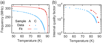
Finally, we probe the resonances of Samples A and C at a variable temperature. Here, the cooling is mediated by He exchange gas. The extracted and are the most sensitive to when the devices are just below (Fig. 4). We compare the frequency data to an analytical model Lee et al. (2005); Sato et al. (2018):
| (5) |
where is the lowest in the dataset, and . For both samples, the best fits of this form have K and [Fig. 4(a)]. On the other hand, we deduce that becomes dominantly limited by the intrinsic rf losses when it drops below near [Fig. 4(b)].
In conclusion, we have demonstrated high- kinetic inductance magnetometers with a sensitivity of at kHz and K. They tolerate background fields of T, which is close to the Earth’s field. We anticipate that changing the sensor geometry by implementing narrow constrictions Asfaw et al. (2018) to reduce should allow for periodical resets, enabling operation at even higher fields. The constrictions should also help to increase the kinetic inductance fraction, a likely route towards a higher device responsivity. Considering the sensitivity, we would find useful a further study of the cause of the low-frequency noise, and methods to minimize it. Future investigations of the YBCO KIM could also evaluate the possibility of beating the 200-mT limit of the perpendicular background field of the NbTiN KIM Asfaw et al. (2018).
Acknowledgements.
We thank Maxim Chukharkin for fabricating Sample A, Paula Holmhund for help in sample preparation, and Juho Luomahaara and Heikki Seppä for valuable discussions. V.V., H.S., M.K. and J.H. acknowledge financial support from Academy of Finland under its Center of Excellence Program (project no. 312059), and grants no. 305007 and 310087. S.R., A.K., D.W. and J.S. acknowledge financial support from the Knut and Alice Wallenberg Foundation (KAW2014.0102), the Swedish Research Council (621-2012-3673) and the Swedish Childhood Cancer Foundation (MT2014-0007). We acknowledge support from Swedish national research infrastructure for micro and nano fabrication (Myfab) for device fabrication.References
- Timofeev et al. (2017) A. Timofeev, J. Luomahaara, L. Grönberg, A. Mäyrä, H. Sipola, M. Aikio, M. Metso, V. Vesterinen, K. Tappura, J. Ala-Laurinaho, A. Luukanen, and J. Hassel, IEEE Transactions on Terahertz Science and Technology 7, 218 (2017).
- Lindeman et al. (2014) M. A. Lindeman, J. A. Bonetti, B. Bumble, P. K. Day, B. H. Eom, W. A. Holmes, and A. W. Kleinsasser, Journal of Applied Physics 115, 234509 (2014).
- Ho Eom et al. (2012) B. Ho Eom, P. K. Day, H. G. LeDuc, and J. Zmuidzinas, Nature Physics 8, 623 (2012).
- Ranzani et al. (2018) L. Ranzani, M. Bal, K. C. Fong, G. Ribeill, X. Wu, J. Long, H. S. Ku, R. P. Erickson, D. Pappas, and T. A. Ohki, arXiv:1809.11048 [quant-ph] (2018).
- Wang et al. (2018) G. Wang, C. L. Chang, S. Padin, F. Carter, T. Cecil, V. G. Yefremenko, and V. Novosad, Journal of Low Temperature Physics 193, 134 (2018).
- Rantwijk et al. (2016) J. v. Rantwijk, M. Grim, D. v. Loon, S. Yates, A. Baryshev, and J. Baselmans, IEEE Transactions on Microwave Theory and Techniques 64, 1876 (2016).
- Sato et al. (2018) K. Sato, S. Ariyoshi, S. Negishi, S. Hashimoto, H. Mikami, K. Nakajima, and S. Tanaka, Journal of Physics: Conference Series 1054, 012053 (2018).
- Luomahaara et al. (2014) J. Luomahaara, V. Vesterinen, L. Grönberg, and J. Hassel, Nature Communications 5, 4872 (2014).
- Asfaw et al. (2018) A. T. Asfaw, E. I. Kleinbaum, T. M. Hazard, A. Gyenis, A. A. Houck, and S. A. Lyon, Applied Physics Letters 113, 172601 (2018).
- Sipola et al. (2018) H. Sipola, J. Luomahaara, A. Timofeev, L. Grönberg, A. Rautiainen, A. Luukanen, and J. Hassel, arXiv:1810.03848 [physics] (2018).
- Ghirri et al. (2015) A. Ghirri, C. Bonizzoni, D. Gerace, S. Sanna, A. Cassinese, and M. Affronte, Applied Physics Letters 106, 184101 (2015).
- Faley et al. (2017) M. I. Faley, J. Dammers, Y. V. Maslennikov, J. F. Schneiderman, D. Winkler, V. P. Koshelets, N. J. Shah, and R. E. Dunin-Borkowski, Superconductor Science and Technology 30, 083001 (2017).
- Zmuidzinas (2012) J. Zmuidzinas, Annual Review of Condensed Matter Physics 3, 169 (2012).
- Vissers et al. (2015) M. R. Vissers, J. Hubmayr, M. Sandberg, S. Chaudhuri, C. Bockstiegel, and J. Gao, Applied Physics Letters 107, 062601 (2015).
- Vissers et al. (2010) M. R. Vissers, J. Gao, D. S. Wisbey, D. A. Hite, C. C. Tsuei, A. D. Corcoles, M. Steffen, and D. P. Pappas, Applied Physics Letters 97, 232509 (2010).
- Ghigo et al. (2004) G. Ghigo, D. Botta, A. Chiodoni, R. Gerbaldo, L. Gozzelino, F. Laviano, B. Minetti, E. Mezzetti, and D. Andreone, Superconductor Science and Technology 17, 977 (2004).
- Hattori, Yoshitake, and Tahara (1998) W. Hattori, T. Yoshitake, and S. Tahara, IEEE Transactions on Applied Superconductivity 8, 97 (1998).
- (18) See supplementary material.
- Megrant et al. (2012) A. Megrant, C. Neill, R. Barends, B. Chiaro, Y. Chen, L. Feigl, J. Kelly, E. Lucero, M. Mariantoni, P. J. J. O’Malley, D. Sank, A. Vainsencher, J. Wenner, T. C. White, Y. Yin, J. Zhao, C. J. Palmstrøm, J. M. Martinis, and A. N. Cleland, Applied Physics Letters 100, 113510 (2012).
- Sun, Gallagher, and Koch (1994) J. Z. Sun, W. J. Gallagher, and R. H. Koch, Physical Review B 50, 13664 (1994).
- Zaitsev et al. (2002) A. G. Zaitsev, R. Schneider, G. Linker, F. Ratzel, R. Smithey, P. Schweiss, J. Geerk, R. Schwab, and R. Heidinger, Review of Scientific Instruments 73, 335 (2002).
- Wang et al. (2003) L. M. Wang, C.-C. Liu, M.-Y. Horng, J.-H. Tsao, and H. H. Sung, Journal of Low Temperature Physics 131, 551 (2003).
- Krupka et al. (1994) J. Krupka, R. Geyer, M. Kuhn, and J. Hinken, IEEE Transactions on Microwave Theory and Techniques 42, 1886 (1994).
- Buckley, Agnew, and Pells (1994) S. N. Buckley, P. Agnew, and G. P. Pells, Journal of Physics D: Applied Physics 27, 2203 (1994).
- Taber and Flory (1995) R. C. Taber and C. A. Flory, IEEE Transactions on Ultrasonics, Ferroelectrics, and Frequency Control 42, 111 (1995).
- Lee et al. (2005) J. H. Lee, W. I. Yang, M. J. Kim, J. C. Booth, K. Leong, S. Schima, D. Rudman, and S. Y. Lee, IEEE Transactions on Applied Superconductivity 15, 3700 (2005).