\marginsize
3cm3cm3cm1cm
Signal Formation in THGEM-like Detectors
Purba Bhattacharyaa∗1, Luca Molerib, Shikma Bresslera
a Department of Particle Physics and AstroPhysics, Weizmann Institute of Science, Herzl St. 234, Rehovot - 7610001, Israel
b Department of Physics, Technion - Israel Institute of Technology, Haifa - 3200003, Israel
Abstract
Numerical simulations were used to study signal formation in a Thick Gaseous Electron Multiplier (THGEM) and in THGEM -based Thick-WELL (THWELL) and Resistive-Plate WELL (RPWELL) detectors. The signal shapes were simulated in mixtures of Argon and Neon with Methane under irradiation with soft x-rays and muons. Anode-induced raw signals were convoluted with the response functions of charge-sensitive and current-sensitive pre-amplifiers. The simulation toolkit was validated by the good agreement reached between the simulated and measured response, with different pre-amplifiers. It indicates that our simulations framework provides valid insight into the inherent complex dynamical processes of the various detectors.
Keywords: THGEM-based Detectors, Anode-induced Signals, Charge and Current-Sensitive Pre-Amplifiers, Convoluted Signals
∗Corresponding Author: Purba Bhattacharya
E-mail: purba.bhattacharya85@gmail.com
1 Introduction
Signals resulting from radiation-induced charges in gaseous radiation detectors, drifting under electric field and multiplied in a gas-avalanche mode - provide information on the deposited energy and position of the interacting event. The current induced on a specific electrode by a drifting charge can be calculated from the Shockley-Ramo Theorem [1, 2]. The induced charge in the detector is constant along its drift path, under an applied electric field. The shape of the currents induced by drifting electrons and ions, depends on the detector type and geometry, on the electric-field distribution and on the charge mobility in a given gas [3, 4, 5, 6].
Charge-sensitive preamplifiers are often used to provide an output voltage pulse of amplitude proportional to the integral of the varying-in-time input current pulse. The output pulse can be obtained by convoluting the input current with the pre-amplifier’s response (transfer function). For more details see [4, 5].
In this work, we have used Garfield [7, 8] in combination with neBEM [9, 10], Magboltz [11, 12] and Heed [13, 14] software packages for evaluating the signal formation in some Thick Gaseous Electron Multiplier (THGEM)-like detectors [15, 16]: standard THGEM, Thick WELL (THWELL) [17] and Resistive-Plate WELL (RPWELL) [18]. Their schematic descriptions are shown in Figure 1. They share similar geometrical and material features.
A comprehensive comparison of their simulated signal shapes is presented in this work and compared to experimental results. Note that similar framework was used in the past for simulating the signal shapes in Micromegas [19] and RPC [20] detectors. In the process of evaluating the signal shapes from the THGEM-based detectors, we have also convoluted the raw signals with the transfer functions of the different pre-amplifiers employed to reproduce the experimental conditions.
The detector geometries are discussed in section 2. The simulation method is detailed in section 3. The experimental setup is described in section 4, followed by the results in section 5 and a discussion in section 6.
2 THGEM-based Detectors
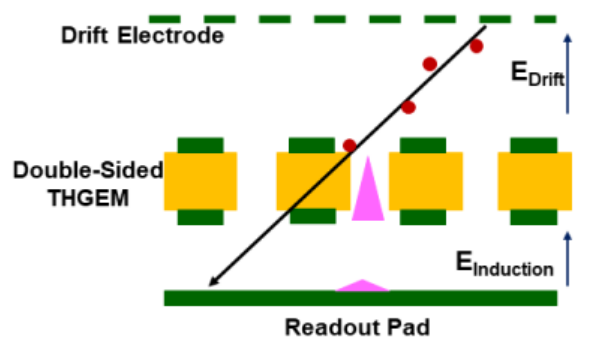
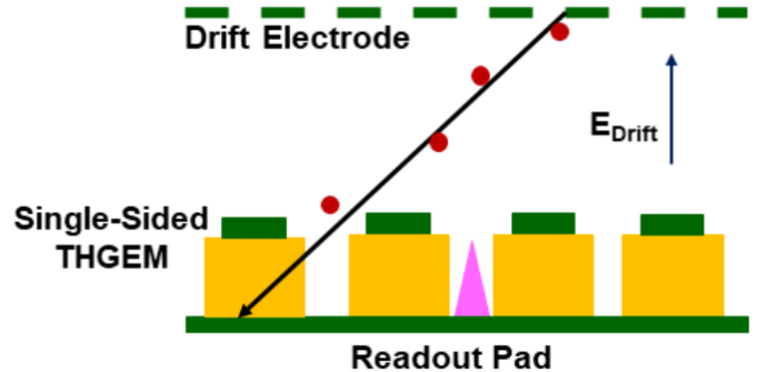
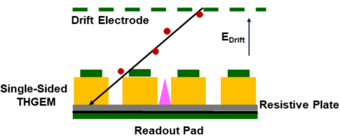
The THGEM [15, 16, 21, 22] is a simple and robust detector suitable for applications requiring large-area detection surfaces with moderate spatial resolution ( RMS). In its original configuration, a THGEM electrode is made of a thick double-sided printed-circuit board (Cu-clad on both surfaces) having mechanically-drilled holes typically in diameter with chemically etched rims, patterned over the surface with pitch (Fig. 1a). Single-sided THGEM electrodes (copper-clad on its top side only) are used for WELL configurations, in which a readout anode is coupled directly (THWELL, Fig. 1b) or via resistive material (Resistive WELL [17] and the RPWELL (Fig. 1c)) to the multiplier’s bottom surface. The resistive coating of the anode of its coupling through a resistive plate aim at quenching occasional discharges. A stable operation of RPWELL detectors in muon- and hadron-beams, was demonstrated in neon- and argon-based gas mixtures [23, 24, 25, 26].
In its standard configuration (Figure 1), the THGEM electrode is preceded by a conversion and drift gap. Radiation-induced ionization electrons drift into the THGEM holes, where multiplication occurs under a high electric field. The resulting avalanche electrons are extracted into a few-mm wide induction gap and drift towards the readout anode, inducing a signal. As long as the field strength in the induction gap is below the multiplication threshold, the induced signal (measured on the readout anode) is characterized by a fast rise time (of a few ). The anode is sensitive essentially only to the motion of avalanche electrons along the induction gap; the ion movement occurs within the THGEM hole, far from the anode, and has a negligible effect on the pulse shape [27]. In the THWELL (Figure 1), higher gains could be obtained at a given applied voltage across the THGEM electrode, due to the larger electric field within the closed holes. The signal induced on the THWELL anode plate is characterized by a fast rise (avalanche electrons) followed by a slow avalanche-ion component [27]. In the RPWELL, the electrode is coupled to a thin plate of high bulk resistivity (), with the patterned readout anode placed behind [18]. Despite of the additional Resistive Plate (RP), the pulse shape on the anode is similar to that of the THWELL [18, 27].
| Detector | Thickness | Gas Mixture | Voltage [V] |
|---|---|---|---|
| THGEM | 2000 | ||
| THGEM | 1600 | ||
| THWELL | 1700 | ||
| THWELL | 1200 | ||
| RPWELL | 1750 | ||
| RPWELL | 975 | ||
| RPWELL | 1250 | ||
| RPWELL | 850 |
In the present work, three types of detectors were investigated: 1) and thick double-sided single THGEM detectors (with induction gap), 2) and thick THWELL detectors and 3) and thick RPWELL detectors. In the RPWELL, the resistive plate (RP) consisted of a thick Semitron ESD225 static dissipative acetal material with a bulk resistivity of [28]. In all of the cases, the hole diameter and pitch are and , respectively. Avalanche electrons in the RPWELL holes, traversing the RP are evacuated to ground through the RP bottom surface - coated with a thin layer of graphite (surface resistivity ) [26]. The geometrical and voltage configurations of the investigated detectors are summarized in Table 1. The drift gap in all configurations was kept at , with spacers between the cathode mesh and the multiplier’s top electrode; the drift field in all experiments was . The THGEM detector was operated with a wide induction gap (Figure 1), under an induction field of (below charge multiplication onset).
3 Numerical Model
Garfield simulation framework [7] has been used in the present work. The 3D electrostatic field simulations have been carried out with the neBEM (nearly exact Boundary Element Method) toolkit [9]. HEED [13] has been used for primary-ionization calculations and Magboltz [11] - for computing drift, diffusion as well as Townsend and attachment coefficients.
The design parameters of the THGEM-based detectors considered in the numerical simulations are those described in section 2. The RP of the RPWELL detector was considered to be a dielectric - transparent to the signals induced on the anode [29]. The basic electrode’s cell structure has been repeated along both X- and Y-axes, to represent a real detector. The field configurations of the different detectors have been simulated using the voltage settings mentioned in Table 1.
Primary-electron clusters were generated for 5.9 keV photons and relativistic muons interacting with the detector medium; the latter being distributed along a track portion depositing energy within the drift gap (Fig. 2). The primary-electrons’ drift process towards the THGEM electrode was simulated using the Microscopic tracking routine [7]. In this procedure, a typical drift path proceeds through millions of collisions, each being classified as elastic or inelastic (including excitation, ionization, attachment etc.). The electrons are focused into the holes by the drift- and the hole’s dipole fields, inducing avalanches within the holes. In this process, an electron starting from a given point is subject to collisions with gas molecules; at each step, a number of secondary electrons are produced according to the local Townsend and attachment coefficients; the newly produced electrons are traced like the initial ones. In parallel, the ions’ drift lines are traced.
In a medium with perfect conductors and insulators, the current induced by a moving charge onto an electrode can be calculated by means of the Shockley-Ramo theorem [2, 3]. The current that flows into one particular electrode under the influence of a charge moving with velocity can be calculated using the following equation:
| (1) |
Here is the field created by raising this electrode to a potential and grounding all other electrodes, in the absence of charge.
The total charge induced on the electrode is given by
| (2) |
is the weighting potential difference across which the charge has drifted.
We used the Shockley-Ramo theorem to calculate the induced current on a uniform readout anode. The current pulse was then convoluted with the readout electronics response function. The output voltage from the preamplifier is then:
| (3) |
4 Experimental setup
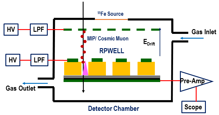
The experimental setup in lab, is shown in Figure 3. The investigated detectors were placed in an aluminum vessel flushed with and at a flow of 25 sccm (standard cubic centimeters per minute) at atmospheric pressure. The detectors were investigated at the Laboratory with -source 5.9 KeV x-rays and cosmic muons; complementary measurements with an RPWELL detector were carried out at CERN-SPS with 150 GeV muons.
The drift electrode and the multiplier’s top electrode (and bottom electrode in the case of the THGEM) were polarized, through low-pass filters, by CAEN N1471H HV power supplies. In all configurations, the anode was at ground potential. In the laboratory studies, anode signals (in the THGEM configuration readout-anode signals after the induction gap) were recorded through a charge-sensitive pre-amplifier (Canberra 2006; decay-time of ) and a custom-made fast current pre-amplifier having shaping time of . The preamplifier signals were processed by an Agilent Technologies InfiniiVision DSO-X 3034A digital oscilloscope. In all detector configurations, the voltage values across the multiplier (Table 1) were adjusted to keep similar gas gains of .
In the CERN-SPS (H2 RD51 Test Beam area) accelerator measurements, the signal shapes of a thick RPWELL detector were studied in . The signal pulses were recorded by an APV25 fast current pre-amplifier chip [30] (shaping time of ); they were further processed and digitized by an SRS readout system [31]. The latter has been frequently used to characterize the performance of MPGD detectors [32, 33], including the THGEM and RPWELL ones [23, 24].
5 Results
5.1 Response to 5.9 keV photons
5.1.1 Simulated Raw Current Signals
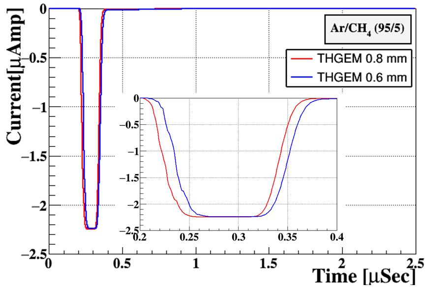
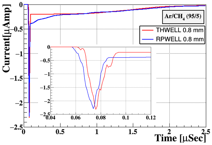
Typical simulated x-ray-induced raw current signals in the THGEM detector (Figure 1) are shown in Figure 4 for and thick electrodes. The induced currents are due to the movement of avalanche electrons extracted from the hole, along the induction gap - towards the readout-anode plate. In this configuration, there are no ions drifting along the induction gap (no slow ion component). The signal length dictated by electron drift along the induction gap is ; the thickness variation does not affect this time by more than .
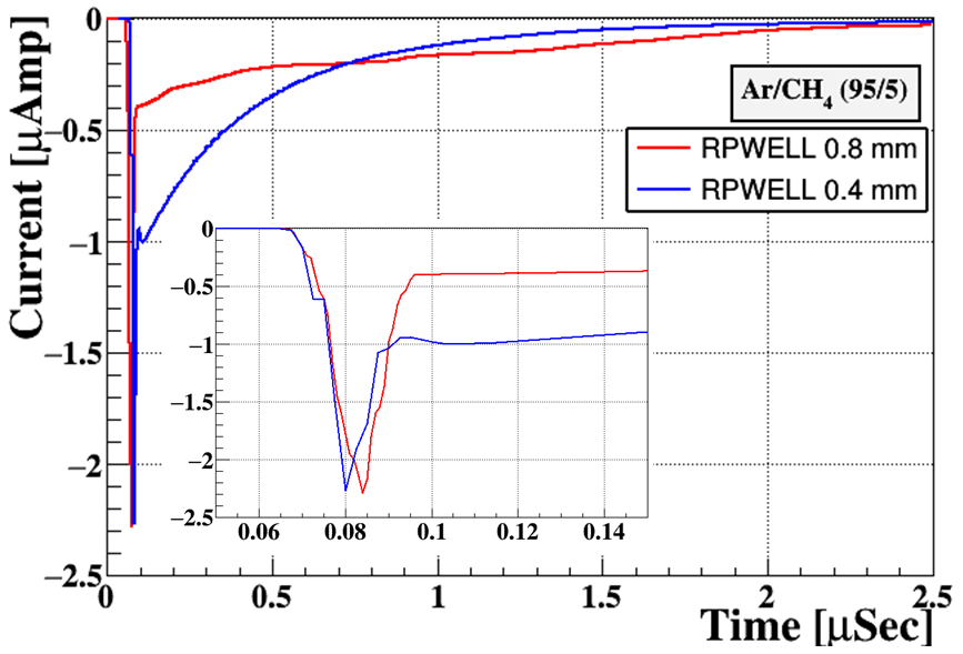
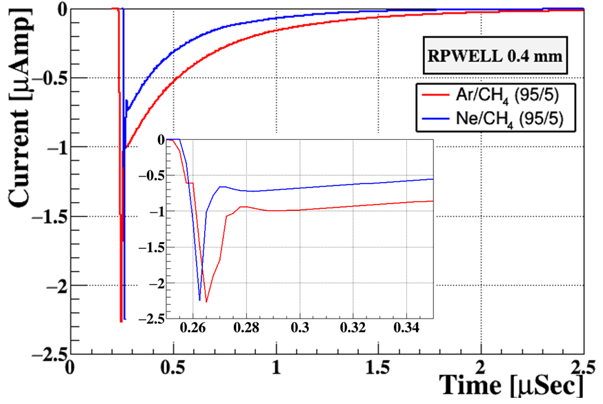
The raw current signals of the THWELL and RPWELL detectors are shown in Figure 4; the fast pulse is due to the avalanche electrons, whereas the long tail is the result of the ions’ drift away from the avalanche head. The RPWELL current signals are peaked similarly to that of the THWELL; however, the ion-component shape is different in both detectors. Due to the presence of the resistive layer (Figure 1), the weighting field in the RPWELL is different from that of the THWELL detector. But, in both cases, the ion tail reaches zero value within . The raw current signal of RPWELL detectors having thickness of and are shown in Figure 4. The rise-time for the thick electrode is , whereas for thick one it is . Throughout this paper, the time required for the response to rise from to of its maximum value is defined as the rise time of the signal . The decay time of the ion tail for the thicker electrode is in comparison to for the thinner one, consistent with the shorter ion drift time to the top electrode. A comparison of the raw signals of a thick RPWELL detector in and is shown in Figure 4. The ion tail in the Ne-mixture decays faster than that in the Ar-mixture; it is consistent with the faster ion velocity in the former.
5.1.2 Charge-sensitive Pre-amplifier response: Measurements and Simulations
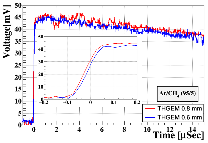
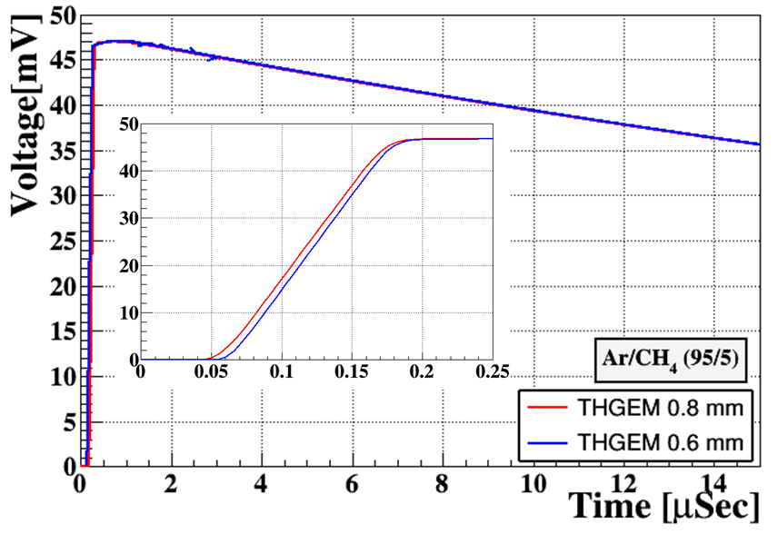
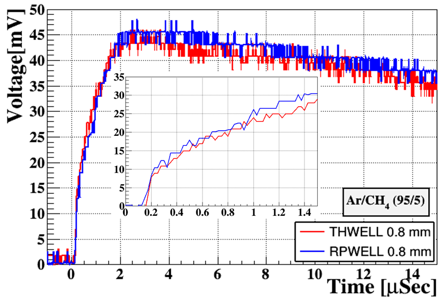
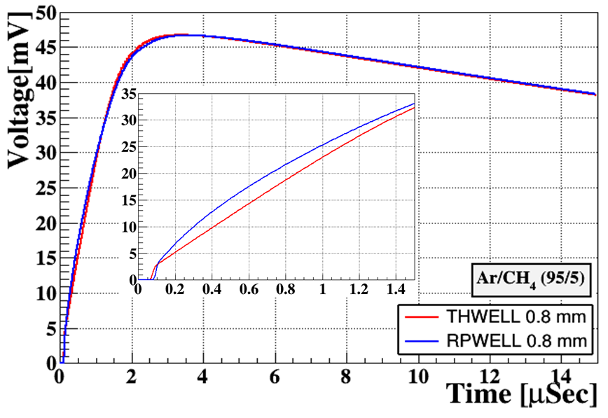
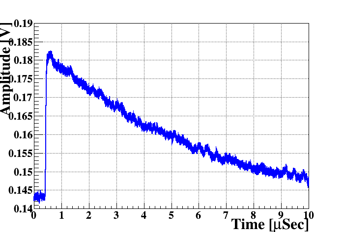
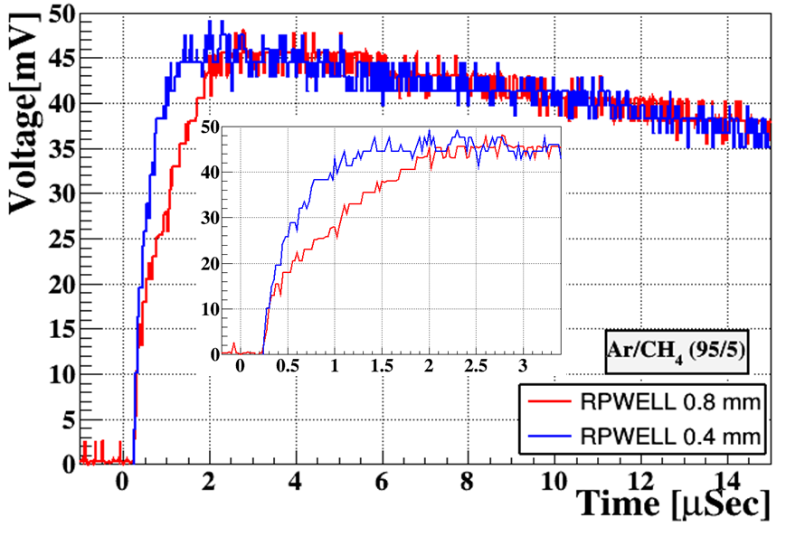
Charge-sensitive pre-amplifier signals measured on the anodes of the THGEM are shown in Figures 5(a). The rise-time of the THGEM pulse, reflecting the avalanche-electrons drift to the anode, is . The respective simulated charge signal is shown in Figures 5(b). As discussed in Section 3, the raw current signals (Figure 4) are convoluted with the response function of the pre-amplifier. The decay time, determined by the decay constant of the pre-amplifier, is long, of the order of few tenths of . A comparison of the measured and simulated charge-signal shapes of THWELL and RPWELL detectors are shown in Figure 6. There is no significant difference in the signal shapes. The RPWELL detectors pulses have and rise for respective electrode thicknesses of and (longer ion drift time along the holes) as shown in Figure 7. In all the above cases, the simulated data are in good agreement with the experimental data.
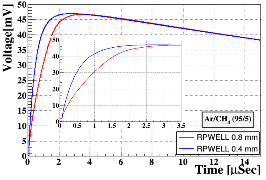
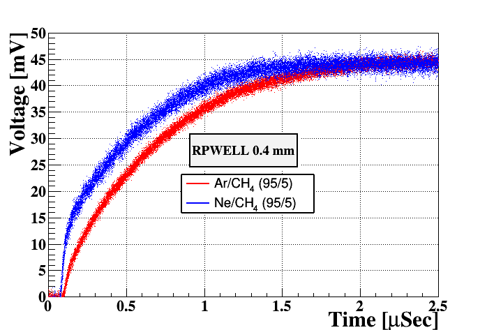
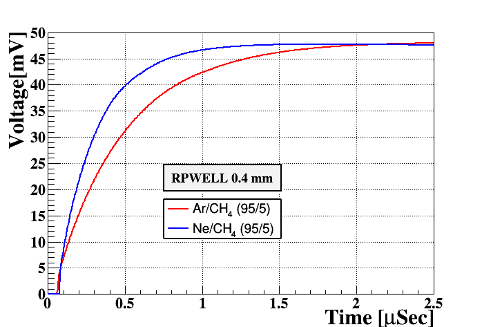
A comparison of the measured and simulated signal shapes of the thick RPWELL detector in and in are shown in Figure 8. The simulated ion-component rise-time in the Ne mixture is faster than that in the Ar one, which is consistent with the fast ion mobility in Ne-based gas mixture. The experimental signals (8) are in good agreement with the simulated ones (8).
5.1.3 Current Pre-amplifier response: Measurements and Simulations
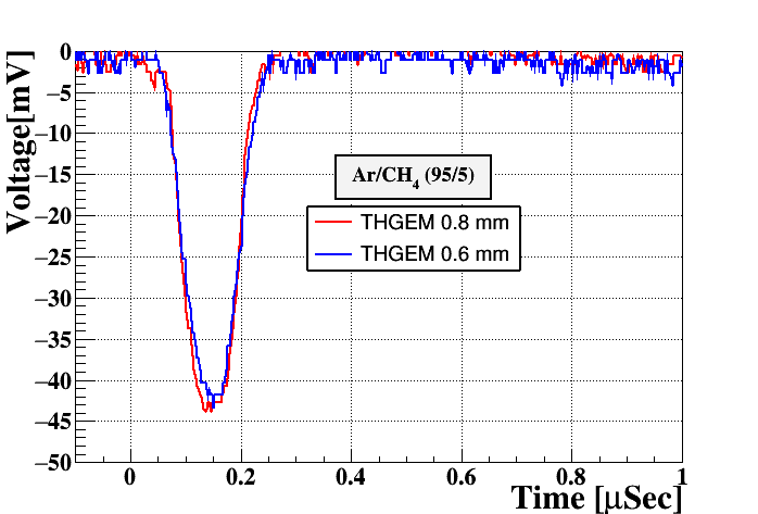
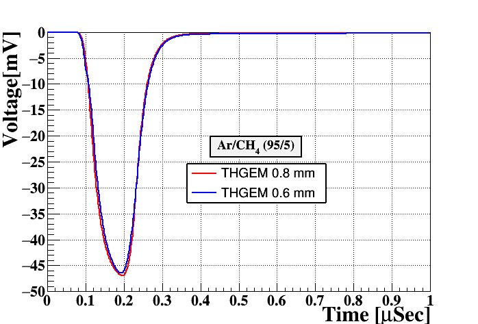
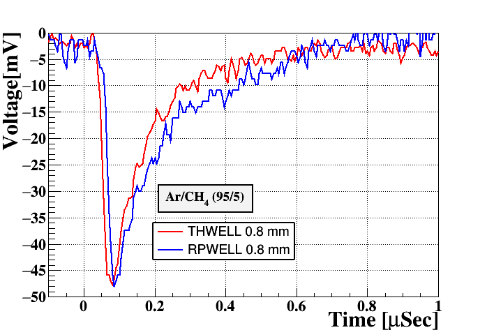
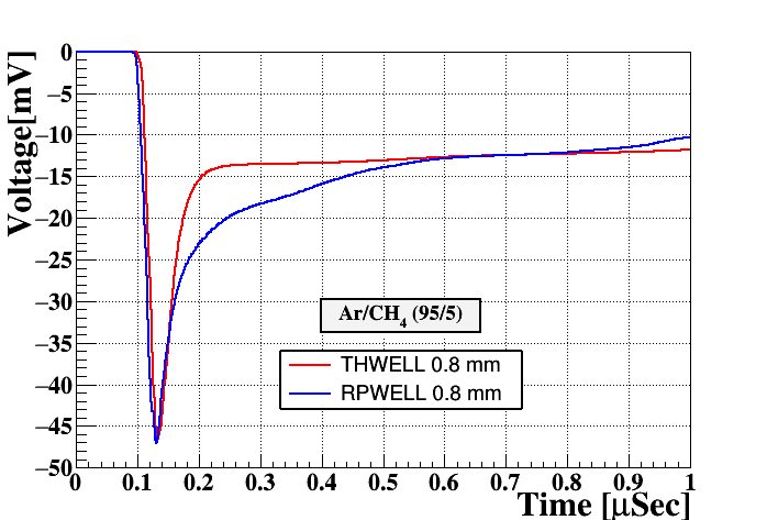
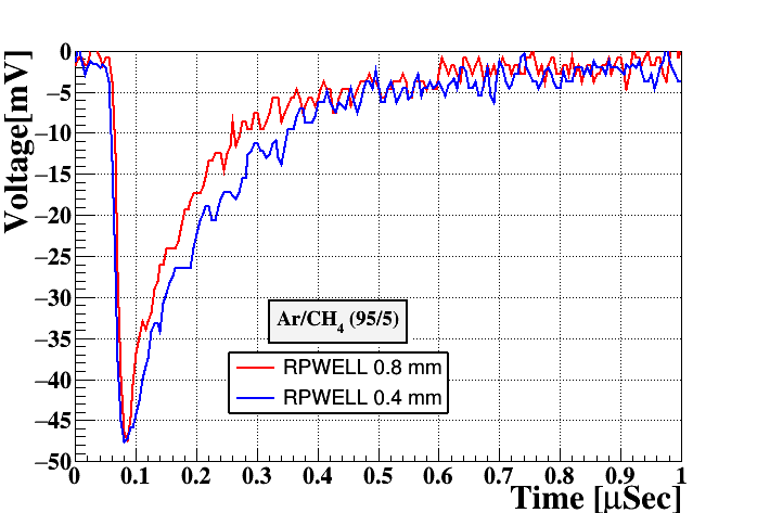
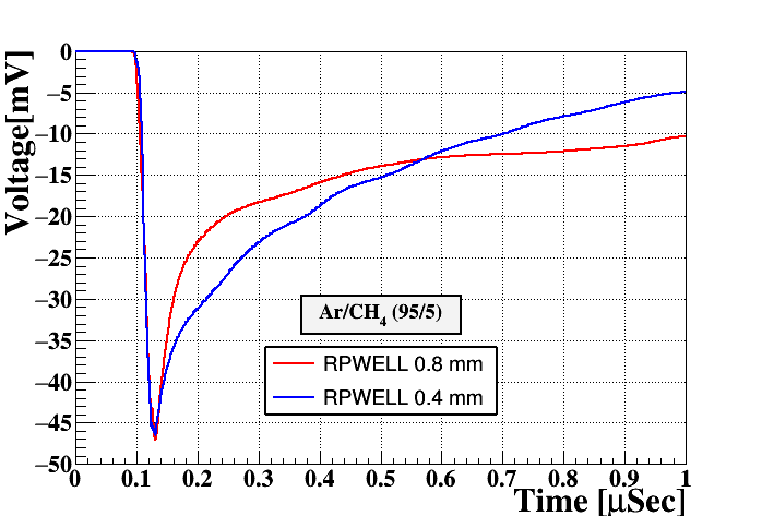
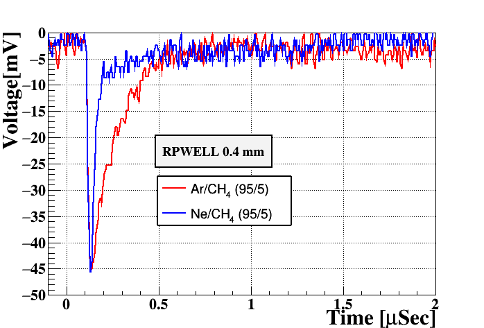
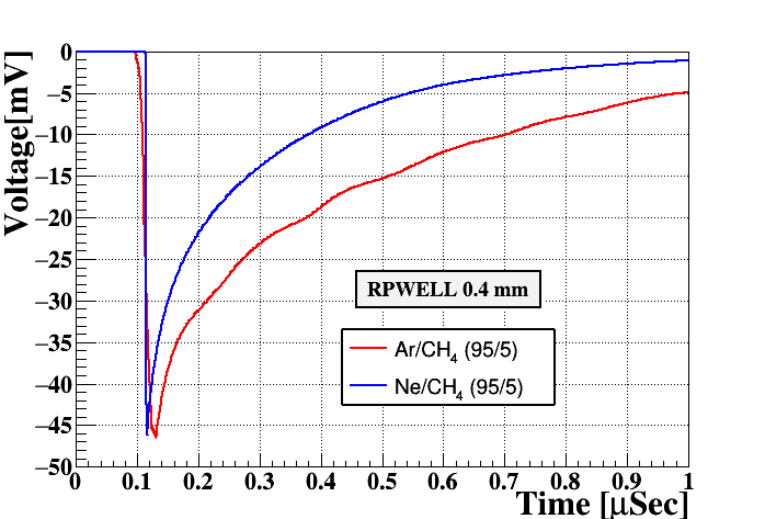
The measured and simulated fast-current signals induced by x-rays in THGEM detector, recorded with the custom-made current-sensitive pre-amplifier are shown in Figure 9. Due to the pre-amplifier shaping time, the THGEM pulses have a rise-time of and a width of (electron drift time within the induction gap). A comparison of measured and simulated fast current-signal shapes, recorded with the custom-made current preamplifier, in thick THWELL and RPWELL detectors are shown in Figure 10. The THWELL and RPWELL detectors pulses are narrower; they have a faster rise-time, of . The current peak is followed by a long ion tail, more pronounced in the simulation than in the measurement. The electrode thickness does not affect the signals’ rise time of RPWELL detectors as shown in Figure 11. The effect of the gas mixture on the signal shape in the RPWELL detector is shown in Figure 12.
5.2 Response to Cosmic Muons: Measurements and Simulations
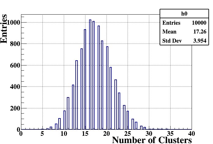
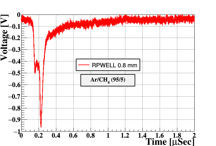
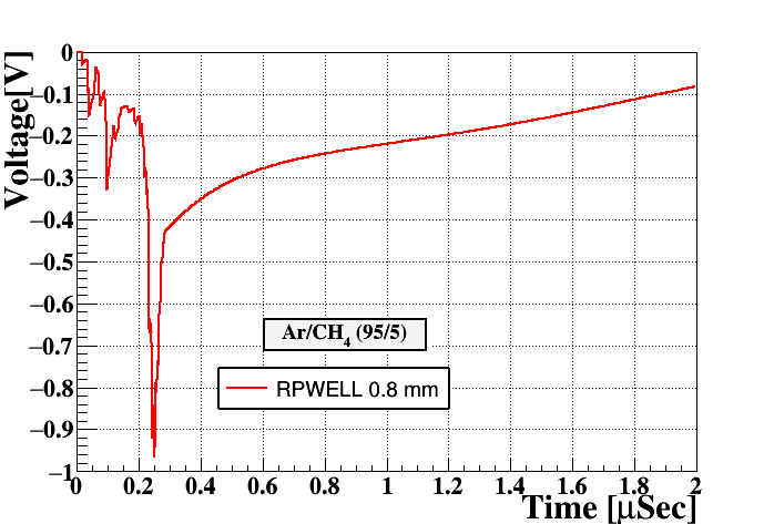
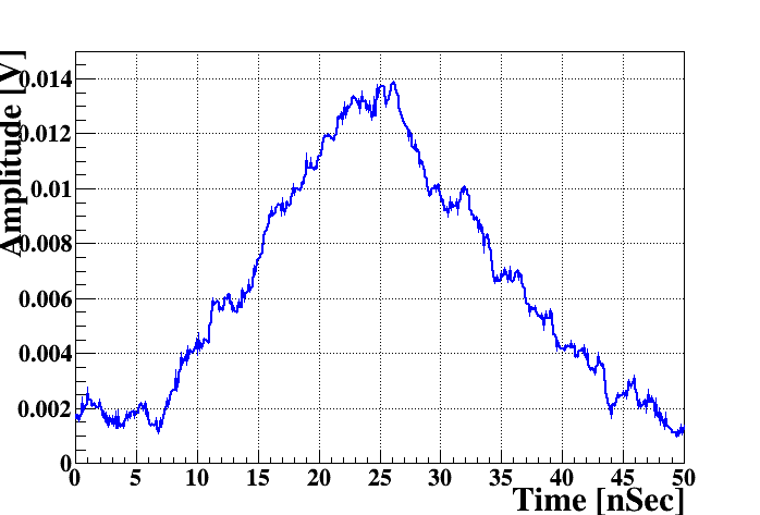
While the soft x-ray photons induce local electron clusters in each interaction in the drift gap, cosmic muons induce extended ionization charges along their tracks; a computed distribution of ionization clusters within the gap is shown in Figure 13. The electron drift time from a cluster positioned close to a hole could be at the order of a few ; others, drifting to the hole from distant locations generate trains of signals during a few . Due to its long shaping time, a typical signal of a charge-sensitive pre-amplifier will consist of fast electron-component signals on top of the long ion-component. Signals from a current-sensitive pre-amplifier exhibit cluster-induced peaks as shown in Figure 13 (measured) and 13 (simulated).
5.3 Response to accelerated Muons: Measurements and Simulation
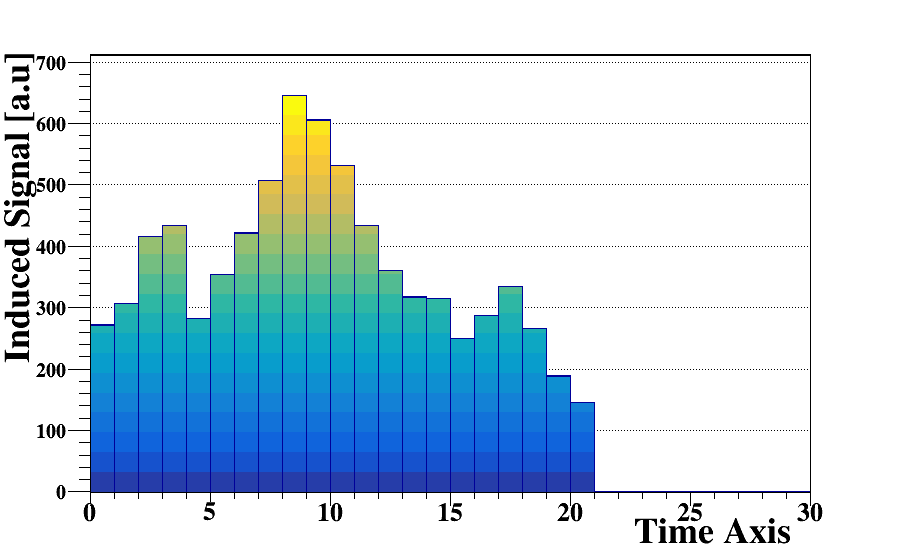
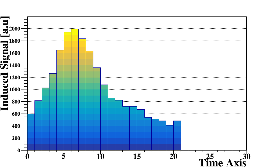
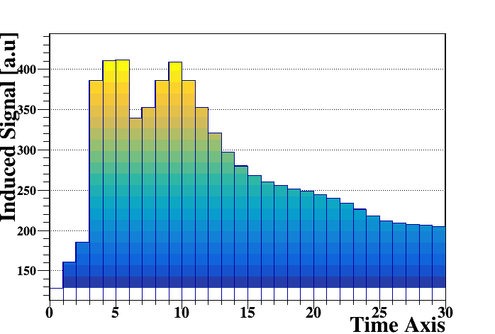
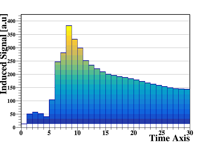
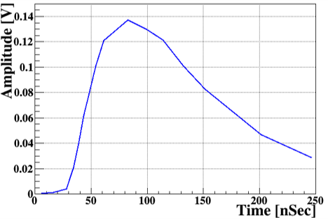
We implemented our numerical model to simulate the signal shape measured with the APV25 chip, having shaping time. Operated in ambient gas, the thick RPWELL detector (of ) has been investigated with muons (normal incidence) at CERN-SPS. The signal shapes varied from track to track, according to the number of primary clusters and their location within the long drift gap. As an example, two measured signals are shown in Figures 14 and 14. In these measurements, we used a strip-patterned readout anode and the signal was induced on a few neighboring strips [34]. For simplicity, in the simulation we assumed a continuous-non-patterned anode. A comparison of the shape of the signals induced on the central strip with the simulated one shows similar characteristics (Figure 14 and 14).
6 Discussion
An evaluation of the signal formation in THGEM -like detectors is presented. The model-simulated signal shapes in THGEM (with induction gap), THWELL and RPWELL were validated by experimental results . The simulations were performed combining Garfield and neBEM packages. The signal shapes have been simulated in and in under irradiation with 5.9 keV x -ray photons, cosmic and relativistic muons. The raw signals were convoluted with the pre-amplifiers’ response functions; the final signal forms were compared to that of measured signals in the three detector configurations investigated.
The soft-photon “point ionization” signals, measured by a fast preamplifier, differ from the “extended ionization” clustered muon-induced ones. The “clustering” effect is washed out using charge-sensitive pre-amplifiers of long shaping time; it is clearly observed with a fast current-pre-amplifier and with the APV25 chip having short shaping times. The difference between the signals in - and -based gas mixtures is reflected by the length of the ion-component tail (measured with a charge preamplifier); it is shorter in the -based gas - due to higher ion mobility. The fast pre-amplifier, of shaping time, integrates only of the total charge. This effect should be taken into account when evaluating the detector gain. The variation of the detector thickness affects the slow ion’s signal rise-time (with a charge-sensitive pre-amplifier), whereas the fast current (electrons mostly) signal does not reveal any significant change in the signal shape.
The effect of the RP is visible by comparing the ion component of the raw signal of the RPWELL to that of the THWELL. This affect is washed out when measuring with the charge sensitive pre-amplifier having long shaping time but is visible while using the fast pre-amplifier of short shaping time.
To summarise, rather good qualitative agreement was reached between the simulated and measured signal shapes, in all configurations investigated, under all irradiation conditions and gas mixtures. This confirms the success of the developed simulation tool - taking into account the important physics processes affecting the signal formation in these detectors as well as the response of the readout electronics. The model and the simulation kit provide a solid tool for conducting similar studies in other gas-avalanche detector configurations.
7 Acknowledgment
We thank Dr. R. Veenhof and Prof. S. Mukhopadhyay for their valuable suggestions and comments. This research was supported in part by the I-CORE Program of the Planning and Budgeting Committee, the Nella and Leon Benoziyo Center for High Energy Physics at the Weizmann Institute of Science and by Grant No 712482 from the Israeli Science Foundation (ISF).
References
- [1] W. Shockley, Jour. Applied Phys. 9 (1938) 635.
- [2] S. Ramo, Proc. IRE, IEEE 27 (1939) 584.
- [3] W. Blum, W. Riegler, L. Rolandi, Edition (Springer, New York, NY) (2008).
- [4] G. F. Knoll, Edition, John Willey Sons.
- [5] F. Sauli, Cambridge Monographs on Particle Physics, Nucl. Phys. and Cosmology.
- [6] Kristen A. Recine, James B. R. Battat, Shawn Henderson, American Jour. Phys. 82 (2014) 322.
- [7] http://cern.ch/garfield.
- [8] R. Veenhof, Nucl. Instr. Meth., A 419 (1998) 726.
- [9] http://cern.ch/neBEM.
- [10] N. Majumdar, S. Mukhopadhyay, Jour. Instr. 2 (2007) P09006.
- [11] http://cern.ch/magboltz.
- [12] S.F. Biagi, Nucl. Instr. Meth. A 421 (1999) 234.
- [13] http://cern.ch/heed.
- [14] I.B. Smirnov, Nucl. Instr. Meth. A 554 (2005) 474.
- [15] R. Chechik, A. Breskin, C. Shalem, D. , Nucl. Instr. Meth. A 535 (2004) 303.
- [16] A. Breskin et al., Nucl. Instr. Meth. A 598 (2009) 107.
- [17] S. Bressler, L. Arazi, L. Moleri, M. Pitt, A. Rubin, A. Breskin, Jour. Instr. 8 (2013) C12012.
- [18] A. Rubin, L. Arazi, S. Bressler, L. Moleri, M. Pitt, A. Breskin, Jour. Instr. 8 (2013) P11004.
- [19] P. Bhattacharya, S. Mukhopadhyay, N. Majumdar, S. Bhattacharya, Nucl. Instr. Meth. A 793 (2015) 41.
- [20] A. Jash, N. Majumdar, S. Mukhopadhyay, S. Saha, S. Chatttopadhyay Jour. Instr. 11 (2016) C09014.
- [21] M. Alexeev et al., Jour. Instr. 5 (2010) P03009.
- [22] M. Alexeev et al., Nucl. Instr. Meth. A 639 (2011) 130.
- [23] S. Bressler et al., Jour. Instr. 11 (2016) P01005.
- [24] L. Moleri et al., Nucl. Instr. Meth. A 845 (2017) 262.
- [25] S. Bressler et al., Jour. Instr. 8 (2013) P07017.
- [26] L. Moleri et al., Jour. Instr. 11 (2016) P01093.
- [27] L. Arazi, M. Pitt, S. Bressler, L. Moleri, A. Rubin, A. Breskin, Jour. Instr. 9 (2014) P04011.
- [28] https://www.quadrantplastics.com/na-en/products/engineering-plastics/advanced-325-425-f/semitron-R-semiconductor-grade-products
- [29] W. Riegler, Nucl. Instr. Meth. A 491 (2002) 258.
- [30] M. J. French et al., Nucl. Instr. Meth. A 466 (2001) 359.
- [31] S. Martoiu, H. Muller, A. Tarazona, J. Toledo, Jour. Instr. 8 (2013) C03015.
- [32] K. Gnanvo et al., IEEE Nucl. Sci. Symp. Conf. Rec. (2010) 552.
- [33] V. et al., Jour. Instr. 7 (2012) T06001.
- [34] L. Moleri, P. Bhattacharya, A. E. C. Coimbra, A. Breskin, S. Bressler, Jour. Instr. 12 (2017) P10017.