figurec
Transmission across a bilayer graphene region
Abstract
The transmission across a graphene bilayer region is calculated for two different types of connections to monolayer leads. A transfer matrix algorithm based on a tight binding model is developed to obtain the ballistic transmission beyond linear response. The two configurations are found to behave similarly when no gate voltage is applied. For a finite gate voltage, both develop a conductance gap characteristic of a biased bilayer, but only one shows a pronounced conductance step at the gap edge. A gate voltage domain wall applied to the bilayer region renders the conductance of the two configurations similar. For a microstructure consisting of equally spaced domain walls, we find a high sensitivity to the domain size. This is attributed to the presence of topologically protected in-gap states localized at domain walls, which hybridize as the domain size becomes of the order of their confining scale. Our results show that transmission through a bilayer region can be manipulated by a gate voltage in ways not previously anticipated.
I Introduction
The unique band structure of graphene gives rise to several alluring phenomena which have been the subject of intense research since its experimental discovery in 2004 (Novoselov et al., 2004; Geim and Novoselov, 2007; Geim, 2009; Castro Neto et al., 2009). In particular, its high charge-carrier mobility has rendered graphene a highly attractive and promising component for electronic and optoelectronic devices (Avouris, 2010; Xia et al., 2013). Another appealing feature of graphene for device application is its stability at the nanometer scale, ensured by the covalent bonds among the carbon atoms (Chen et al., 2008), which is highly desirable for device-miniaturization. A graphene-based electronic device, entirely made out of micro-structured graphene sheets, is thus expected to reduce significantly energy dissipation and optimize device-miniaturization and functionality (Eda and Chhowalla, 2009; Georgiou et al., 2013; Jang et al., 2016). The recent realization of a short channel field-effect transistor, using just 9- and 13-atom wide graphene nanoribbons (Llinas et al., 2017), is a convincing step in that direction. This is to be contrasted with mainstream semiconductor technology which usually integrates different materials and where component-interfacing can be difficult to scale-down (Schwierz, 2010).
Although a gapless conductor, the versatility of the electronic properties of graphene make it possible to easily induce a gap. This can be done by several means: cutting it into nanoribbons with zigzag or armchair edges (Son et al., 2006; Han et al., 2007; Chen et al., 2007; Wakabayashi et al., 2009); by breaking inversion symmetry with an appropriate substrate (Zhou et al., 2007); or applying an out-of-plain electric filed in graphene bilayer structures (Castro et al., 2007, 2008, 2010; Zhang et al., 2009).
Compared to monolayer graphene, the possibility of tuning the induced gap by an external, perpendicular electrical field, which is easily introduced through a gate potential, makes the bilayer more suitable for device applications (McCann and Koshino, 2013). Not only the gap can be tuned by a gate bias, but also a twist angle can be engineered between the two layers (Li et al., 2010; Luican et al., 2011). This leads to a strong reconstruction of the band structure at low energies (Amorim, 2018). The recent observation of superconductivity and insulating behavior in twisted bilayer graphene at the magic angles clearly shows the high degree of tunability of this system (Cao et al., 2018a, b). Further manipulation of the bilayer response is possible by inserting an insulator between the two graphene layers, out of which tunnel field effect transistors have been realized (Mishchenko et al., 2014; Georgiou et al., 2013; Britnell et al., 2012a, b; Amorim et al., 2016; Chen et al., 2018).
One other advantage of the graphene bilayer is that its electronic structure of can manipulated by a layer-selective potential, induced by a gate voltage. The possibility of sharply reversing the sign of voltage, thus creating a well-defined one-dimensional boundary separating regions of constant potential, has been demonstrated recently (Li et al., 2016). These domain walls support confined one-dimensional states that are topologically protected and can be used as purely one-dimensional channels (Martin et al., 2008; Koshino, 2013).
The ballistic transport across a bilayer graphene region has been studied at length (Snyman and Beenakker, 2007; Nilsson et al., 2007; Barbier et al., 2009; Nakanishi et al., 2010; González et al., 2010, 2011; Chu et al., 2017). Particular attention has been given to a setup where a gate voltage is applied within the bilayer region (Nilsson et al., 2007; Barbier et al., 2009; González et al., 2011; Chu et al., 2017). These studies already revealed a high degree of tunability of the transport properties. However, the effects of further manipulations of the gate voltage, namely through the creation of a domain wall affecting the bilayer region (Li et al., 2016) are yet to be investigated. Furthermore, the possibility of a microstructured gate voltage with several built-in domain walls opens up new avenues to engineer electronic transport at the nanoscale.
The aim of this paper is to study ballistic transport of micro-structured bilayer graphene flakes of with different types of connection to monolayer. Using a tight-binding model of an AB staked bilayer flake, taken to be infinite in the transverse direction, we observe that the conductance displays aperiodic oscillations as a function of chemical potential. The conductance in the presence of a single voltage domain is shown to be compatible with previous results obtained within a low energy approximation. We compute the conductance in the presence of a domain wall in the gate bias and show that, in this case, geometries with different types of connection to monolayer leads behave similarly. We further study the effect of a micro-structured gate bias with multiple domain walls. By changing the separation between domain-walls we explore the crossover form well separated domain-wall states to the fully hybridized regime where in-gap states start to contribute to the conductance. Finally, we have studied the viability of an integrated nano-transistor for experimentally reasonable conditions finding that this setup can achieve on/off ratios of the output current within .
The structure of the paper is as follows: in Sec. II, we introduce the model of the physical setup and the corresponding tight-binding formulation as well as the method for obtaining the transmission across the bilayer region using the transfer matrix formulation. In Sec. III, some representative results of transmission are presented, including the new types of micro-structured gated bilayer graphene. Sec. IV contains a short summary and the conclusions. In Sec. A, we present some of the details of the calculation of the transmission.
II Model and methods
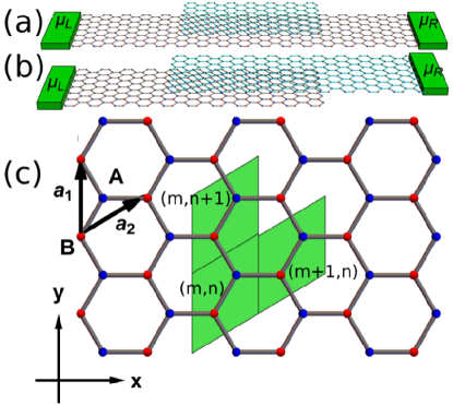
Schematics of the setup for which the transmission and the conductance are studied is shown in Fig. (1). The case of Fig. 1(a) consists of a single layer graphene with a flake of another layer on top, the setup. The second configuration is obtained from two sheets of graphene that are partially overlapped, the setup, as shown in Fig. 1(b). In both we consider A-B stacking. Translational invariance along the transverse direction (-axis) is presumed. We are interested in the ballistic regime where the electronic mean free path is larger than the typical length of the device. For simplicity, we consider the case of perfect contacts, which can be replaced by infinite leads.
We model electrons in the structure using the conventional tight-binding approach for electrons (Castro Neto et al., 2009) hopping between nearest neighbor carbon sites of the atomic lattice shown in Fig. (1)(c), which can be written as . Here,
| (1) | ||||
| (2) |
is the Hamiltonian of the layer, and
| (3) |
is the inter-layer hopping term, with the creation operators of a particle in sublattice in the unit cell of the th layer. The effect of an applied gate voltage within the bilayer region is modeled by . The BL restriction in the summation stands for sites belonging to the bilayer region.
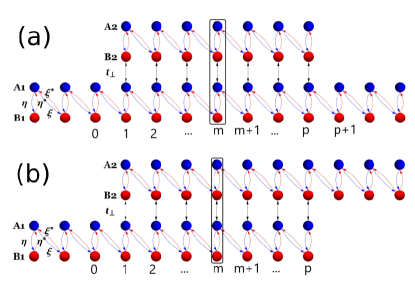
After Fourier transformation in the direction, the stationary states of the 1D effective chain for the two cases shown in Fig. (2) can be written as
| (4) |
with the wave number along the direction. Within the monolayer (lead) region, we define the column vector which obeys the transfer matrix equation (see Appendix A),
| (5) |
where is given by
| (6) |
with and . For the bilayer region () we define obeying
| (7) |
where the transfer matrix is given by
| (12) |
The amplitudes at the left and the right interfaces can be related by,
| (13) |
and by the boundary conditions: for the case, and for the case, as can be seen in Figs. 2(a) and 2(b). With these boundary conditions one obtains the matrix relating the layer 1 in the left to layer 1(2) in the right,
Within the semi-infinite leads, Eq. (5) can be solved by assuming the ansatz
with . The eigenvalues and the eigenmodes are explicitly derived in Appendix A. In the leads we only consider propagating modes, so that . The eigenmodes are thus interpreted as left-moving, , and right-moving, , modes, according to their group velocity (see Appendix A). We then use the eigenbasis to write the wave function in the leads,
| (15) |
| (16) |
from which we define transmission and reflection coefficients, respectively and . The transmission and reflection coefficients are given by,
| (17) |
where .
The transmission probability is then defined as , and the overall transmission per transverse unit length is given by,
| (18) |
Using the Landauer formula (Datta, 2005), we find the current per transverse unit length across the bilayer region,
| (19) |
where is the Fermi distribution function and () are the chemical potential in the left (right) lead (in the following we assume ). Assuming , with , we can linearize the Landauer formula (Büttiker et al., 1985) to obtain the conductance , which can be written as
| (20) |
where is the conductance quantum. For a system at zero temperature, Eq. (20) can be simplified to .
III Results and Discussion
III.1 Transmission through a bilayer graphene region
In this section, we compute the transmission amplitudes for the and cases. A simplifying feature is that, for both cases, there is only one propagating incident mode associated with given , hence the corresponding transfer matrix of the leads is a two by two. Note that, due to electron-hole symmetry, .
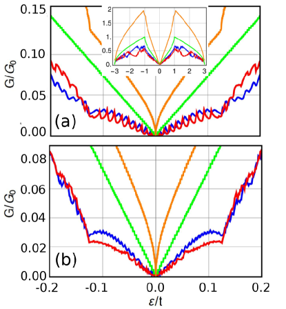
Figure 3 shows the conductance for energies near the Fermi-level for the (blue) and (red) geometries and for two values of the scattering region size, , (a), and for , (b). For comparison, the conductance through an infinite system consisting of a single (green) or a double (orange) graphene layer is also depicted. Note that, in these cases the total transmission in Eq. (18) is simply determined by the dispersion relation. Therefore, for low energies it behaves as for the single layer and as for the bilayer.
For both geometries, the low energy conductance is almost twice as low as for pristine graphene and vanishes faster, with a scaling behavior. The inset of Fig. 3(a), depicting for the all energies within the bandwidth, shows that, even away from the Fermi-level, never attains the value of the pristine case.
Another pronounced low energy feature of the transmission, is the sudden increase for energies around . Thus, as also seen in the pristine double layer case, the conductance resolves the appearance of the higher energy band, after which two propagating modes become available for transport within the bilayer region.
The differences between the and geometries are more pronounced for higher energies. At low energies, they can be completely masked out by the finite-size effects that yield the characteristic jumps in the conductance, Fig. 3(a). For larger values of , when the finite-size oscillations are reduced, the case is seen to have a higher conductance. This is to be expected since in this case, the transmitted electrons do not have to change layer, which is suppressed for low values of .
III.2 Conductance through a gated bilayer graphene region
III.2.1 Homogeneous case
In this section, we study the effect on the transmission of a gate voltage applied within the bilayer region. We assume that only one of the layers is affected by the gate while the other remains at zero voltage. We study the cases for which the voltage of the lower, , or upper layers, , is or ten times larger , which correspond to typical values of gate voltages that can be implemented experimentally.
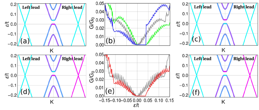
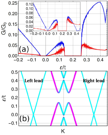
Fig. 4 shows the conductance through a gated bilayer graphene region in different cases together with a plot of the band structure of the bilayer and the single layer leads around zero energy (computed assuming an infinite system).
Fig. 4(b) depicts the geometry for and (blue) and for the swapped voltage configuration and (green). The most pronounced features are the suppression of transport for and a jump in the conductance for seen in 4(b) blue, which is not present when the gate voltages are swapped in 4(b) (green). The illustrations of the band structures in Figs. 4(a) and 4(c) help to understand this behavior. The effect of the gate voltage is to open up a gap in the dispersion relation of the bilayer. Moreover, while for , the wave-function’s amplitudes are equally distributed between the two layers of the bilayer system, for finite voltages their distribution changes drastically near the gap edges (valence band maximum and conduction band minimum). The color coding in Fig. 4(a) and 4(c) shows the localization of the wave-function in the upper or lower layers. This energy-dependent layer distribution can simply explain the conduction jump: in the case depicted in 4(a), after passing the energy gap the system has suddenly available a large density of transmission modes within the lower layer. Such matching conditions (same color, at a given energy, for the leads and the bilayer region) never arises in the opposite case, 4(b) green, as can be seen in 4(c).
Figs. 4(e) depicts the transmission for the geometry. This case is symmetric under the swapping of the voltages. In this case Figs. 4(d) and 4(f) show that the perfect matching conditions seen in 4(a) are never attained and thus no jump in conductance is observed.
The conductance attained when the gate voltage is increased by one order of magnitude is depicted in Fig. 5(a) for the two geometries (blue) and (red) for and . The inset shows the voltage swapped case, and . Fig. 5(b) depicts the band structure, with the same color coding as before, corresponding to the case and and . An interesting feature of the transmission in Fig. 5(a) is that there are two regions where the conduction seems to vanish. One, at higher energies, corresponds to the band-gap and thus the suppression of the conductance is not surprising. However, the second arises within a region where the density of states is finite. Again, the plot of the band structure in Fig. 5(b) can simply explain this effect: the gap in conductance corresponds to a region where the conducting states with support on the lower layer become gapped, so although the total density of states is finite, there are no states contributing to transport.
III.2.2 Inhomogeneous case: single domain wall
In this section, we study how the transmission is affected by the presence of an inhomogeneous gate voltage. We consider the simplest case where a gate voltage domain wall is present in the bilayer region. We assume that the local potential at cell , layer (see Fig. 2) is given by , with the Heaviside function. Therefore, the potential difference on the left half ( is while on the right half () it is , which implies a domain wall right at the middle of the bilayer region. This domain wall structure is known to support confined states, localized in the transverse direction and extending along the wall (Martin et al., 2008), with important consequences regarding transport in the direction of the wall (Li et al., 2016). The impact of a domain wall on charge transport in the perpendicular direction has not been studied before and is analyzed in the following.
In Fig. 6 we show the conductance for the geometries (blue) and (red) for . The two geometries now have very similar conductance, which contrasts with the case when no domain wall is present, depicted in Figs. 4(b) and 4(f). A noticeable difference is the absence of the jump in conductance observed for the geometry in Fig. 4(b). Since the domain wall reverses the layer distribution of the wave-function’s amplitudes, the perfect matching conditions seen in 4(a) are never attained and thus no jump in conductance is observed. We conclude that the domain wall erases the difference between the two geometries.
As shown in Ref. (Martin et al., 2008), the states confined at the domain wall originate one-dimensional bands dispersing inside the bulk gap. In Fig. 6 the impact of those states is unnoticeable, as a well resolved gap of order is still apparent. This can be understood as a consequence of transverse confinement. At low energies, the wave function of these states has a decay length of the order , where is the carbon-carbon distance (Martin et al., 2008). For the decay length is , much smaller than the distance between the domain wall and the edges of the scattering region. Therefore, for a single domain wall, these states do not contribute in propagating charge across the bilayer region.
III.3 Conductance through a microstructured biased bilayer graphene region
We now generalize our study to multiple domain walls. Our aim is to show how these microstructures, that are now routinely fabricated, can be used to engineer the transmission. We consider the potential of the previous section generalized for a periodic gated region of size , , where
and . As a function of , there are two qualitatively different cases that we consider in the following: a large domain length, , where the edge modes along the domain wall do not hybridize and thus do not contribute to the transport properties; and a small domain length, , for which there is hybridization of edge modes and thus transport for energies within the bulk gap becomes possible.
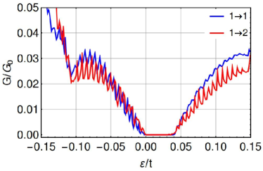
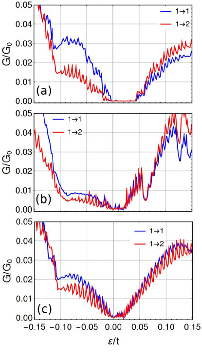
Figure 7 shows the evolution of the conductance curves with . We consider, as before, corresponding to . In Fig. 7(a) we show the conductance for . As for the case in the previous section, the differences between the two geometries are not significant and there is almost no conductance within the gap, for .
Figure 7(b) depicts the conductance for a smaller value of . Here, there are already some states within the gap that contribute to transport which result from the hybridization of the edge modes along the domain walls.
In Fig. 7(c) we set , for which the domain wall states are already fully hybridized. Note the striking similarity between the low energy conductance and that obtained for an unbiased bilayer region, shown in Fig. 3 and as a background in Figs. 4(b-c) and 4(f-g). It is clear that the effect of the gap has been completely washed out. At higher energies, however, the system still shows the conductance asymmetry typical of a gate biased bilayer region [see Figs. 4(b-c) and 4(f-g)].
III.4 Results for current at finite temperature and device application
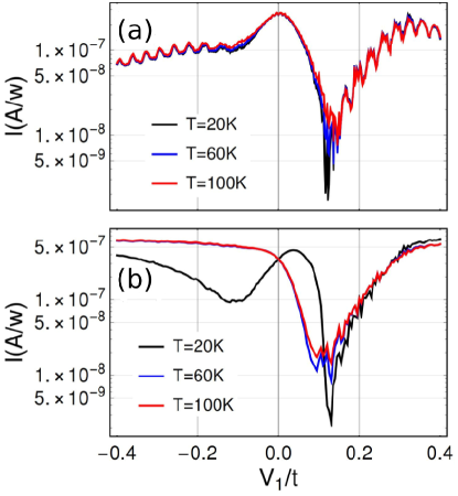
In this section, we study the viability of an integrated nano-transistor based on the or geometries.
For this device, one aims to maximize the current ratio between the “on” and “off” currents, and , passing through the terminals, when changing between two values of the applied gate voltage. Due to its low resistance and versatility, graphene is a natural candidate for transistor implementations. However, due to the nature of its band structure, achieving a high on/off ratio is a technical challenge especially at finite temperature. We exploit the non-linear behavior of the conductance obtained with the setup of Fig. 4(b) to optimize the and study its behavior at finite temperature.
Figure (8) shows the logarithmic plot of the current for the , panel (8)(a), and , panel (8)(b), setups for different temperatures as a function of gate voltage . The chemical potentials on the left and right leads were fixed at the experimentally reasonable values of . In the gate voltage interval this setup can achieve .
IV Conclusion
In this work, we have studied the conductance across a graphene bilayer region for two different positions of the single layer leads: the case when the leads connect to the same layer, the configuration; and the case when the leads connect to different layers, configuration. We have worked in the limit of an infinitely wide scattering region, to avoid edge effects, and developed a transfer matrix, tight-binding based methodology which allows going away from linear response. We have found that, when there is no gate bias applied to the bilayer region, the two setups, and , have a similar behavior, with a slightly higher conductance in the configuration. The presence of a bias gate voltage differentiates between the two configurations. Both of them develop a conductance gap which mimics the spectral gap of a biased bilayer, but only the configuration shows a pronounced conductance step at one of the gap edges, extending the results obtained in the continuum limit (Nilsson et al., 2007) and for ribbons of finite width (González et al., 2011). This step is not present if the gate polarity is reversed. Introducing a domain wall in the gate bias applied to the bilayer region, the conductance step disappears and the two configurations, and , behave again in a similar way.
We have also studied the effect of a gate bias with a multiple domain wall microstructure applied to the bilayer region. When the separation between domains is much larger than the localization length of the states confined at the domain walls, the multiple domain walls states behave independently and the result is similar to the case of a single domain wall. On decreasing the separation between domain walls, the localized states start to hybridize and a finite conductance starts to appear inside the gap. At even smaller distances, the gap is completely washed out, and only at higher energies a conductance asymmetry characteristic of a gate biased bilayer region is present. Finally, we have studied the viability of an integrated nano-transistor based on the or geometries. For experimentally reasonable chemical potential difference () and gate voltage interval (from 0 up to ) we have found that this setup can achieve . Summing up all the finds, it is clear the transmission through a bilayer region can be manipulated by a gate bias in ways not previously anticipated.
Acknowledgements.
We thanks B. Amorim for valuable discussions. The authors acknowledge partial support from FCT-Portugal through Grant No. UID/CTM/04540/2013. H.Z.O acknowledges the support from the DP-PMI and FCT (Portugal) through scholarship PD/ BD/113649/2015. PR acknowledges support by FCT-Portugal through the Investigador FCT contract IF/00347/2014.Appendix A The transmission through a bilayer region
Here we detail the transfer matrix method used to obtain the transmission coefficient. We apply Fourier transformation,
to the tight-binding Hamiltonian (1) and obtain
| (21) | ||||
where and are defined in the main text.
By multiplying by , for a given lattice point , where stands for position, for layer, and labels sublattices, one obtains, for the leads where or ,
with . We rewrite the latter equations in a matrix equation form as
| (30) |
which is equivalent to Eq. (5).
Similar steps can be taken to build the transfer matrix for the bilayer region where ,
from which we obtain Eq. (7) in matrix form.
By imposing the boundary conditions for setup , and defining , we can re-write Eq. (13) as
| (35) |
or equivalently,
| (36) |
where
Using the boundary condition for the setup , we obtain, after similar steps,
| (37) |
where
The last step is to represent wave amplitudes in the eigenbasis of the transfer matrix of the leads. The characteristic equation for the eigenvalue problem reads,
| (38) |
yielding two eigenvalues,
| (39) |
where , corresponding to the normalized eigenvectors
| (40) |
A mode with positive (negative) group velocity is considered to be the right-moving(+) (left-moving(-)) mode. Recalling that in the leads and using Bloch theorem for the Pristine graphene , where is the conjugate momentum in (propagating) direction, and plugging the latter expression into Eq. (38) we obtain the mode group velocity in the propagating direction as:
| (41) |
References
- Novoselov et al. (2004) K. S. Novoselov, A. K. Geim, S. V. Morozov, D. Jiang, Y. Zhang, S. V. Dubonos, I. V. Grigorieva, and A. A. Firsov, Science (New York, N.Y.) 306, 666 (2004).
- Geim and Novoselov (2007) A. K. Geim and K. S. Novoselov, Nature Materials 6, 183 (2007), arXiv:0702595v1 [cond-mat] .
- Geim (2009) A. K. Geim, Science 324, 1530 (2009), arXiv:0906.3799 .
- Castro Neto et al. (2009) A. H. Castro Neto, F. Guinea, N. M. R. Peres, K. S. Novoselov, and A. K. Geim, Reviews of Modern Physics 81, 109 (2009), arXiv:0709.1163v2 .
- Avouris (2010) P. Avouris, Nano Letters 10, 4285 (2010).
- Xia et al. (2013) F. Xia, H. Yan, and P. Avouris, Proceedings of the IEEE 101, 1717 (2013).
- Chen et al. (2008) H. Chen, M. B. Müller, K. J. Gilmore, G. G. Wallace, and D. Li, Advanced Materials 20, 3557 (2008).
- Eda and Chhowalla (2009) G. Eda and M. Chhowalla, Nano Letters 9, 814 (2009).
- Georgiou et al. (2013) T. Georgiou, R. Jalil, B. D. Belle, L. Britnell, R. V. Gorbachev, S. V. Morozov, Y.-J. Kim, A. Gholinia, S. J. Haigh, O. Makarovsky, L. Eaves, L. A. Ponomarenko, A. K. Geim, K. S. Novoselov, and A. Mishchenko, Nature Nanotechnology 8, 100 (2013), arXiv:1211.5090 .
- Jang et al. (2016) H. Jang, Y. J. Park, X. Chen, T. Das, M.-S. Kim, and J.-H. Ahn, Advanced Materials 28, 4184 (2016).
- Llinas et al. (2017) J. P. Llinas, A. Fairbrother, G. Borin Barin, W. Shi, K. Lee, S. Wu, B. Yong Choi, R. Braganza, J. Lear, N. Kau, W. Choi, C. Chen, Z. Pedramrazi, T. Dumslaff, A. Narita, X. Feng, K. Müllen, F. Fischer, A. Zettl, P. Ruffieux, E. Yablonovitch, M. Crommie, R. Fasel, and J. Bokor, Nature Communications 8, 633 (2017), arXiv:1605.06730 .
- Schwierz (2010) F. Schwierz, Nature Nanotechnology 5, 487 (2010), arXiv:NIHMS150003 .
- Son et al. (2006) Y.-W. Son, M. L. Cohen, and S. G. Louie, Physical Review Letters 97, 216803 (2006), arXiv:0611602 [cond-mat] .
- Han et al. (2007) M. Y. Han, B. Özyilmaz, Y. Zhang, and P. Kim, Physical Review Letters 98, 206805 (2007), arXiv:0702511 [cond-mat] .
- Chen et al. (2007) Z. Chen, Y.-m. Lin, M. J. Rooks, and P. Avouris, Physica E: Low-dimensional Systems and Nanostructures 40, 228 (2007), arXiv:0701599 [cond-mat] .
- Wakabayashi et al. (2009) K. Wakabayashi, Y. Takane, M. Yamamoto, and M. Sigrist, New Journal of Physics 11, 095016 (2009), arXiv:arXiv:0907.5243v1 .
- Zhou et al. (2007) S. Y. Zhou, G.-H. Gweon, A. V. Fedorov, P. N. First, W. A. de Heer, D.-H. Lee, F. Guinea, A. H. Castro Neto, and A. Lanzara, Nat. Mater. 6, 770 (2007).
- Castro et al. (2007) E. V. Castro, K. S. Novoselov, S. V. Morozov, N. M. R. Peres, J. M. B. L. dos Santos, J. Nilsson, F. Guinea, A. K. Geim, and A. H. C. Neto, Physical Review Letters 99, 216802 (2007), arXiv:0611342 [cond-mat] .
- Castro et al. (2008) E. V. Castro, N. M. R. Peres, J. M. B. L. dos Santos, F. Guinea, and A. H. C. Neto, Journal of Physics: Conference Series 129, 012002 (2008), arXiv:1004.5079 .
- Castro et al. (2010) E. V. Castro, K. S. Novoselov, S. V. Morozov, N. M. R. Peres, J. M. B. Lopes dos Santos, J. Nilsson, F. Guinea, A. K. Geim, and A. H. Castro Neto, Journal of Physics: Condensed Matter 22, 175503 (2010), arXiv:0807.3348 .
- Zhang et al. (2009) Y. Zhang, T.-T. Tang, C. Girit, Z. Hao, M. C. Martin, A. Zettl, M. F. Crommie, Y. R. Shen, and F. Wang, Nature 459, 820 (2009), arXiv:0802.2933 .
- McCann and Koshino (2013) E. McCann and M. Koshino, Rep. Prog. Phys. 76, 56503 (2013).
- Li et al. (2010) G. Li, A. Luican, J. M. B. dos Santos, A. H. Castro Neto, A. Reina, J. Kong, and E. Y. Andrei, Nature Phys. 6, 109 (2010).
- Luican et al. (2011) A. Luican, G. Li, A. Reina, J. Kong, R. R. Nair, K. S. Novoselov, A. K. Geim, and E. Y. Andrei, Phys. Rev. Lett. 106, 126802 (2011).
- Amorim (2018) B. Amorim, Physical Review B 97, 165414 (2018), arXiv:1711.02499 .
- Cao et al. (2018a) Y. Cao, V. Fatemi, S. Fang, K. Watanabe, T. Taniguchi, E. Kaxiras, and P. Jarillo-Herrero, Nature 556, 43 (2018a), arXiv:1803.02342 .
- Cao et al. (2018b) Y. Cao, V. Fatemi, A. Demir, S. Fang, S. L. Tomarken, J. Y. Luo, J. D. Sanchez-Yamagishi, K. Watanabe, T. Taniguchi, E. Kaxiras, R. C. Ashoori, and P. Jarillo-Herrero, Nature 556, 80 (2018b), arXiv:1802.00553 .
- Mishchenko et al. (2014) A. Mishchenko, J. S. Tu, Y. Cao, R. V. Gorbachev, J. R. Wallbank, M. T. Greenaway, V. E. Morozov, S. V. Morozov, M. J. Zhu, S. L. Wong, F. Withers, C. R. Woods, Y.-J. Kim, K. Watanabe, T. Taniguchi, E. E. Vdovin, O. Makarovsky, T. M. Fromhold, V. I. Fal’ko, A. K. Geim, L. Eaves, and K. S. Novoselov, Nature Nanotechnology 9, 808 (2014).
- Britnell et al. (2012a) L. Britnell, R. V. Gorbachev, R. Jalil, B. D. Belle, F. Schedin, M. I. Katsnelson, L. Eaves, S. V. Morozov, N. M. R. Peres, J. Leist, A. K. Geim, K. S. Novoselov, and L. A. Ponomarenko, Science 335, 947 (2012a).
- Britnell et al. (2012b) L. Britnell, R. V. Gorbachev, R. Jalil, B. D. Belle, F. Schedin, M. I. Katsnelson, L. Eaves, S. V. Morozov, A. S. Mayorov, N. M. R. Peres, and Others, Nano Letters 12, 1707 (2012b).
- Amorim et al. (2016) B. Amorim, R. M. Ribeiro, and N. M. R. Peres, Physical Review B 93, 235403 (2016), arXiv:1603.04446 .
- Chen et al. (2018) F. Chen, H. Ilatikhameneh, Y. Tan, G. Klimeck, and R. Rahman, IEEE Transactions on Electron Devices 65, 3065 (2018), arXiv:1711.01832 .
- Li et al. (2016) J. Li, K. Wang, K. J. McFaul, Z. Zern, Y. Ren, K. Watanabe, T. Taniguchi, Z. Qiao, and J. Zhu, Nature Nanotechnology 11, 1060 (2016).
- Martin et al. (2008) I. Martin, Y. M. Blanter, and A. F. Morpurgo, Physical Review Letters 100, 036804 (2008).
- Koshino (2013) M. Koshino, Physical Review B 88, 115409 (2013), arXiv:1307.3421 .
- Snyman and Beenakker (2007) I. Snyman and C. W. J. Beenakker, Physical Review B 75, 045322 (2007).
- Nilsson et al. (2007) J. Nilsson, A. H. Castro Neto, F. Guinea, and N. M. R. Peres, Physical Review B 76, 165416 (2007), arXiv:0607343 [cond-mat] .
- Barbier et al. (2009) M. Barbier, P. Vasilopoulos, F. M. Peeters, and J. M. Pereira, Physical Review B 79, 155402 (2009), arXiv:1101.3930 .
- Nakanishi et al. (2010) T. Nakanishi, M. Koshino, and T. Ando, Physical Review B 82, 125428 (2010), arXiv:1008.4450 .
- González et al. (2010) J. W. González, H. Santos, M. Pacheco, L. Chico, and L. Brey, Physical Review B 81, 195406 (2010).
- González et al. (2011) J. W. González, H. Santos, E. Prada, L. Brey, and L. Chico, Phys. Rev. B 83, 205402 (2011).
- Chu et al. (2017) K.-L. Chu, Z.-B. Wang, J. Zhou, and H. Jiang, Chinese Physics B 26, 067202 (2017).
- Datta (2005) S. Datta, Quantum transport : atom to transistor (Cambridge University Press, 2005) pp. 1–404.
- Büttiker et al. (1985) M. Büttiker, Y. Imry, R. Landauer, and S. Pinhas, Physical Review B 31, 6207 (1985).