Energetics of complex phase diagram in a tunable bilayer graphene probed by quantum capacitance
Abstract
Bilayer graphene provides a unique platform to explore the rich physics in quantum Hall effect. The unusual combination of spin, valley and orbital degeneracy leads to interesting symmetry broken states with electric and magnetic field. Conventional transport measurements like resistance measurements have been performed to probe the different ordered states in bilayer graphene. However, not much work has been done to directly map the energetics of those states in bilayer graphene. Here, we have carried out the magneto capacitance measurements with electric and magnetic field in a hexagonal boron nitride encapsulated dual gated bilayer graphene device. At zero magnetic field, using the quantum capacitance technique we measure the gap around the charge neutrality point as a function of perpendicular electric field and the obtained value of the gap matches well with the theory. In presence of perpendicular magnetic field, we observe Landau level crossing in our magneto-capacitance measurements with electric field. The gap closing and reopening of the lowest Landau level with electric and magnetic field shows the transition from one ordered state to another one. Further more we observe the collapsing of the Landau levels near the band edge at higher electric field ( V/nm), which was predicted theoretically. The complete energetics of the Landau levels of bilayer graphene with electric and magnetic field in our experiment paves the way to unravel the nature of ground states of the system.
I Introduction
Bilayer graphene (BLG) provides a unique two-dimensional system in condensed matter physics, where the low energy spectrum is gapless touching at K and K’ points and an external electric field opens up a tunable gap at the valley pointsMcCann and Fal’ko (2006); Ohta et al. (2006). In clean samples the interactions lead to gap opening even without an external electric fieldNandkishore and Levitov (2010a); Freitag et al. (2012) and interesting phases like quantum spin Hall, anomalous quantum HallNandkishore and Levitov (2010b), layer antiferromagnetWang et al. (2013a), and nematicVafek and Yang (2010) states were suggested to be the possible ground state at the neutrality pointZhang and MacDonald (2012). Bilayer graphene is even more interesting in presence of magnetic field due to the additional orbital degeneracy of the lowest Landau level (LL) together with spin and valley degeneracy, resulting in complex quantum Hall states (QHS)Feldman et al. (2009); Maher et al. (2014). The coupling of electric and magnetic field leads to transitions between different spin, valley and orbital ordering leading to unique interaction driven symmetry broken statesLi et al. (2018); Velasco Jr et al. (2014a); Hunt et al. (2017); Maher et al. (2013); Kou et al. (2014); Lee et al. (2014); Freitag et al. (2013); Velasco Jr et al. (2012); van Elferen et al. (2012); Kim et al. (2011); Velasco Jr et al. (2014b). Thus BLG provides an excellent platform to probe the phase transitions between different ordered statesGorbar et al. (2012); LeRoy and Yankowitz (2014); Kharitonov (2012a, b).
There has been extensive studies to find the nature of ordered states in BLG, both theoreticallyKharitonov (2012a, b, c) and experimentallyWeitz et al. (2010); Kim et al. (2011); Lee et al. (2014); Hunt et al. (2017); Zibrov et al. (2017). The model employed in Refs. Kharitonov (2012b); Lee et al. (2014); LeRoy and Yankowitz (2014) shows that at finite magnetic field (), the LLs are spin splitted and the orbital and valley degeneracies are lifted by the application of electric field. However, model employed in Refs.Hunt et al. (2017); Zibrov et al. (2017) showed that at finite both the spin and orbital degeneracies are lifted, and the application of electric field results in lifting the valley degeneracy only. However, there is no common consensus about the order of the ground state of these symmetry broken statesMaher et al. (2013); Kou et al. (2014); Hunt et al. (2017).
Recent transport measurements in dual gated geometry have observed the crossing of LLs leading to the closing of gap which is attributed to the phase transition between different type of ordered statesWeitz et al. (2010); Kim et al. (2011). Although transport measurements can provide an indication of the gap size, but the true energetics of these states cannot be estimated by conventional transport measurements. Therefore, thermodynamic measurement is desirable to directly probe the electronic properties as well as the energetics of the these statesMartin et al. (2010). The proper knowledge of the energetics of these LL crossing points together with the variation of LL energy by external electric and magnetic fields provide key insights to the nature of ground state, which has been employed to probe the magnetization of quantum hall statesDe Poortere et al. (2000) and many body enhanced susceptibilityZhu et al. (2003) in two dimensional electron gas (2DEG).
In order to obtain the energetics in BLG with electric and magnetic field, we employ magneto capacitance studies in a hexagonal boron nitride (hBN) encapsulated dual gated BLG device. At zero magnetic field, using our quantum capacitance measurement we measure the gap around the charge neutrality point as a function of perpendicular electric field(), where the obtained value of the gap matches well with the previously reported valuesZhang et al. (2009). In presence of perpendicular magnetic field, we observe LL crossing in our magneto-capacitance measurements with . The gap closing and reopening of the lowest LL with and shows the transition from one ordered state to another one. The values of critical electric field () required to close the gap as a function of magnetic field matches well with the earlier reportsWeitz et al. (2010); Kim et al. (2011). We further obtain the energetics of the LLs as a function of and , where the renormalization of LL spectrum at higher electric field ( V/nm) is clearly visible. It has been shown theoretically that at higher electric fields the LLs collapses at the band edge due to LL coupling and hybridization McCann and Fal’ko (2006); Guinea et al. (2006); Ho et al. (2013), which has not been observed experimentally prior to this report.
II experimental details
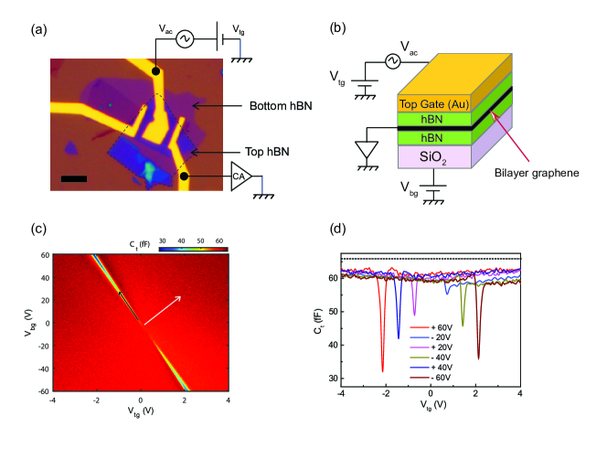
Dual gated bilayer graphene device was fabricated using van der Waals assembly, following the procedure developed by Wang et.al. Wang et al. (2013b). Briefly bilayer graphene (BLG) was first mechanically exfoliated onto a piranha cleaned Si/SiO2 substrate from bulk single crystal of natural graphite. On another clean substrate hBN was mechanically exfoliated and potential thin hBN was looked for using optical microscope. Using dark field microscope imaging hBN flake with uniform smooth surface and free of bubbles was chosen. hBN, BLG and hBN were picked up sequentially one on top of another and the complete stack (hBN-BLG-hBN) was deposited onto a doped Si/SiO2 substrate with 285 nm oxide. The stack was then annealed at 200∘C in vacuum to get a uniform surface free of bubbles. The electrical contacts were fabricated using electron beam lithography followed by etching the hBN-BLG-hBN stack, and one-dimensional contact was established by thermally evaporating Cr/Au (5nm/70nm)Wang et al. (2013b). Another step of lithography and thermal deposition was carried out to define the topgate electrode (see supplemental material; SM-Sec.I for details). The optical image of the final device is shown in Fig. 1a. The schematic of the device and the measurement scheme are shown in Fig. 1b. The top hBN thickness 11 nm and bottom hBN thickness 15 nm were measured using atomic force microscope (see SM-Sec.II). The thickness of top hBN was found independently using period of oscillation of the capacitance minima in magnetic field Yu et al. (2013). The excellent dielectric properties of hBN serves the purpose of using thin gate dielectric for measuring detectable change in total capacitance (Ct). All the measurements were carried out in a 3He refrigerator with a base temperature 240 mK.
For the capacitance measurements we have used the measurement scheme described in our earlier worksKuiri et al. (2015, 2018) using a home built differential current amplifier with a gain of . The capacitance has been measured between the topgate electrode and BLG with a small ac excitation voltage of 10-15 mV at a frequency of 5 kHz with a resolution of . All wires were shielded to reduce the parasitic capacitance. In a parallel plate capacitor made of a normal bulk metal and a two dimensional material like graphene, adding a charge requires electrostatic energy, but also kinetic energy due to the change in chemical potential, thereby contributing to the total capacitanceLuryi (1988). The total measured differential capacitance in such a system is given by
| (1) |
where, is the geometric capacitance, is the quantum capacitance; is the electronic charge; is the area under the topgate electrode; is the thermodynamic compressibility, is the parasitic capacitance arising due to the wirings plus the stray capacitances. In BLG, the application of electric field between the layers results in breaking the inversion symmetry, which in turn opens up a band gap Zhang et al. (2009) at the charge neutrality point. Dual gated geometry allows us to independently control electronic density () and electric displacement field () under the topgated region. The net transverse electric field in a dual gated device is given by and the total carrier density is given by ; is the vacuum permittivity, is the electronic charge, is the capacitance per unit area of the backgate(topgate) region and are the charge neutrality points.
III Capacitance Data at B=0T
Fig. 1c shows the colorplot of the measured total capacitance, as a function of backgate voltage () and topgate voltage () at B = 0T. The data was taken by sweeping the topgate voltage for different values of backgate voltages. Tuning of topgate and backgate changes both the total carrier density () and the band gap (). The diagonal white dashed marked in Fig. 1c shows the direction of and solid black line shows the direction of . For , Ct exhibits a minimum at zero density, signifying the hyperbolic nature of band structure for ungapped bilayer grapheneHenriksen and Eisenstein (2010). As increases the capacitance minima decreases revealing the formation of gap in the energy spectrum in bilayer grapheneYoung et al. (2012). The diagonal line in Fig. 1c corresponds to the charge neutrality point under the topgated region. Along the diagonal line the capacitance minima decreases signifying the electric field induced band gap opening. The charge neutrality points () are located at 0.3V, -8.5V. From the slope of the diagonal line we can effectively estimate the ratio of the capacitive coupling between the top and bottom gates ( along the diagonal line in Fig. 1c, 300 nm, , yields 10.75 nm, which matches well with the value of 11 nm obtained using AFM, see SM-Sec.II). Fig. 1d shows the cut lines of as a function of for several value of . The geometric capacitance is marked with dashed black line. Noting the area of our device , the effective geometric capacitance was . The parasitic capacitance was estimated by comparing the experimental capacitance data at with the theoretical one (Eq.1), where only adjusting parameter was Cp (see SM-Sec.III; the density of states for ungapped bilayer graphene with effective mass was calculated from RefMcCann and Fal’ko (2006)).The parasitic capacitance Cp in our device is 152 fF. This value of Cp is subtracted from all the data presented in this paper.
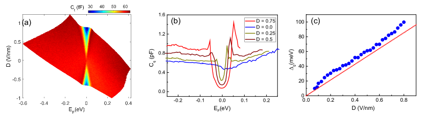
In order to get a better insight to the experimental data we need to extract the quantum capacitance () as a function of Fermi energy () from the experimentally measured as a function of backgate and topgate voltages . The Fermi energy and band gap are independently controlled by changing and . Thus the quantum capacitance should be extracted along the constant lines as a function of Fermi energy. We have followed a similar approach as described in Ref Kanayama and Nagashio (2015) (see SM-Sec.IV for details). The Fermi energy of bilayer graphene is given by the charge conservation relation Dröscher et al. (2010). Fig. 2a shows the colorplot of total capacitance () as a function of Fermi energy and electric field. It can be seen that the band gap opens with the increment of . The maximum we could reach was 0.8 V/nm with a band gap opening 80 meV in agreement with previously reported valuesZhang et al. (2009). The extracted quantum capacitance () for several values of is shown in Fig. 2b. It can be seen that with the increment of , decreases signifying the increase of band gap. We have observed asymmetry in the for the electron and hole side, which has also been previously observed by other groupsYoung et al. (2012); Kanayama and Nagashio (2015). The 1/ van hove singularity is also observed at the band edge as predictedMcCann and Koshino (2013). The extracted as a function of has been shown in Fig. 2c. The measured band gap values matches well with the theoretical band gap calculated using tight binding modelMin et al. (2007).
IV Magneto-capacitance data
The competing magnetic and electric field leads to various interesting phases in the LL spectrum of BLG. To visualize the energetics of the LLs as a function of and B, we present our magneto capacitance data. For an ungapped pristine BLG, in absence of any interactions, the LL energies in a perpendicular magnetic field is given by , where is the cyclotron frequency, and are the orbital index. For . Thus, the zeroth energy LL is eight-fold degenerate, whereas all other landau levels () are four fold degenerate (two spin and two valley)McCann and Fal’ko (2006).
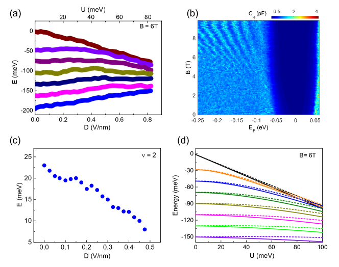
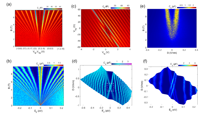
Fig. 3a shows the experimental LL fan diagram for . Here, was measured by sweeping , synchronously keeping the and changing only the carrier density. The dips in the capacitance data corresponds to the LL gap. The gap around the zeroth LL start appearing for . The LL corresponding to can be seen in Fig. 3a. The geometric capacitance Cg was determined independently from the fact that spacing between the adjacent capacitance minima in Fig. 3a is given by the amount of charge required to fill each Landau levelYu et al. (2013) (, where ) (see SM-Sec.V) yielding an effective which matches quite well as extracted from the colorplot of Fig. 1c and AFM imaging (see SM-Sec.II). The conversion of axis in Fig. 3a, which is a combination of topgate voltage and backgate voltage, to Fermi energy is shown in SM-Sec.VI. Fig. 3b shows the result of such a conversion where we plot the extracted as a function Fermi energy for different values of magnetic field. The solid lines are generated using single particle LL energies for ungapped BLG (, with effective mass ). It can be seen that upto , the extracted LL spectrum matches quite well with the theory. However, for we observe noticeable mismatch between the experimental and the theoretical values (10%-20%), which has also been addressed in previous studies, employing magneto-capacitance measurementsYu et al. (2013, 2014); Kuiri et al. (2018). This mismatch has been attributed to the inaccurate conversion in determining at higher magnetic field as the bulk becomes more insulating and increasingly isolated from electrical contacts leading to excess deep in the versus gate voltage curve.
We now show the LL spectrum as a function of electric and magnetic field. Figure. 3c shows the measured as a function of and for . In Fig. 3d we have shown the extracted quantum capacitance as a function of and for B=10T. The parallel lines are the different LLs which evolves with . The most striking feature is the evolution of the zeroth energy LL with . In Fig. 3f we have shown the zoomed part of the Fig. 3d (white dashed box). The emergence of the insulating state can be seen for . With the increment of , we see the evolution of the insulating state. For small values of , state remains gapped, with increase in , the gap decreases monotonically, and then for a critical value mV/nm the gap closes, further increase in the gap again re-opens and remains gapped for high (maximum for our device was 1V/nm). This electric field induced gap closing and re opening is a signature of phase transitionLeRoy and Yankowitz (2014). In Fig. 3e we show the evolution of the state with and . Here, the topgate and backgate were swept synchronously to maintain zero carrier density and vary only as described earlier. The shaped yellow structure in Fig. 3e separate out two insulating states (blue regions inside and outside of the ), which is in consistent with earlier reports. Fig. 4a shows the plot of critical electric field, as a function of B. The , which determines the transition point, can be written as a linear function of magnetic field as , where is the offset electric field and is the slope. For our case and matches well with the theoretically predicted valuesTőke and Fal’ko (2011) and experimentally observed values for reported using resistance measurementsKim et al. (2011), where the QHS undergoes a phase transition between the spin polarized phase and the layer polarized phase in the () plane. Further more the gap at as a function of B is shown in Fig. 4b, where the gap increase linearly with , with a slope of , in agreement with previous reportsMartin et al. (2010), which suggests the ground state is spin polarized () and rules out the possibility that the ground state is valley polarizedKou et al. (2014).
V Landau Levels with high D
Theoretical work employing tight binding calculations have shown that the existence of interlayer bias between the layers () will have compelling effect on the LL spectrum of BLGPereira et al. (2007). In this section we will discuss about the evolution of LL spectrum with high interlayer bias. Figure 5a shows the LL energies as a function of for B=6T. One striking feature is the reduction of the energy separation between the LLs as the band gap increases, specially between the LLs near the band edge. For we see the LLs near the band edge merge with each other. Fig. 5b shows colorplot of LL spectrum (as ) as a function of for (). One can clearly see the differences between the LL spectrum at (Fig. 3b) and (Fig. 5b). At the LLs are clearly visible at B = 2T where as at LLs can be hardly seen even at B = 8T. It can be also seen from the Fig. 5b that the LLs are broadened and the broadening is higher for lower LLs near the band edge. In Fig. 5c, we also show the evolution of the gap for state as a function of for B = 10T. One can notice that for a fixed magnetic field the LLs gap decreases almost linearly with increasing . It has been shown theoretically in RefZhang et al. (2011) that the LL spectrum in presence of B and has the following energy eigenvalues for
| (2) |
where, , , ; is the magnetic length, and is the Fermi velocity. Fig. 5d shows the calculated LL energies as a function of energy gap (U) for B=6T. The solid and the dashed lines correspond to and valleys. The LLs start to merge for which matches well with the experimentally observed values as can be seen in Fig. 5a. We do not observe the splitting of the K and K’ valleys due to the large broadening of our device ( meV). Instead we observe the broadening of the LLs with increasing .
VI conclusion
In summary, we have mapped the complete energetics of the Landau level spectrum in a bilayer graphene with magnetic and electric field. We model a possible ground state based on our observations. We have also demonstrated the smearing of the LLs at high broken inversion symmetry in agreement with theoretical predictions.
References
- McCann and Fal’ko (2006) E. McCann and V. I. Fal’ko, Phys. Rev. Lett. 96, 086805 (2006).
- Ohta et al. (2006) T. Ohta, A. Bostwick, T. Seyller, K. Horn, and E. Rotenberg, Science 313, 951 (2006).
- Nandkishore and Levitov (2010a) R. Nandkishore and L. Levitov, Phys. Rev. Lett. 104, 156803 (2010a).
- Freitag et al. (2012) F. Freitag, J. Trbovic, M. Weiss, and C. Schönenberger, Phys. Rev. Lett. 108, 076602 (2012).
- Nandkishore and Levitov (2010b) R. Nandkishore and L. Levitov, Phys. Rev. B 82, 115124 (2010b).
- Wang et al. (2013a) Y. Wang, H. Wang, J.-H. Gao, and F.-C. Zhang, Phys. Rev. B 87, 195413 (2013a).
- Vafek and Yang (2010) O. Vafek and K. Yang, Phys. Rev. B 81, 041401 (2010).
- Zhang and MacDonald (2012) F. Zhang and A. H. MacDonald, Phys. Rev. Lett. 108, 186804 (2012).
- Feldman et al. (2009) B. E. Feldman, J. Martin, and A. Yacoby, Nature Physics 5, 889 (2009).
- Maher et al. (2014) P. Maher, L. Wang, Y. Gao, C. Forsythe, T. Taniguchi, K. Watanabe, D. Abanin, Z. Papić, P. Cadden-Zimansky, J. Hone, et al., Science 345, 61 (2014).
- Li et al. (2018) J. Li, Y. Tupikov, K. Watanabe, T. Taniguchi, and J. Zhu, Phys. Rev. Lett. 120, 047701 (2018).
- Velasco Jr et al. (2014a) J. Velasco Jr, Y. Lee, Z. Zhao, L. Jing, P. Kratz, M. Bockrath, and C. Lau, Nano Lett. 14, 1324 (2014a).
- Hunt et al. (2017) B. Hunt, J. Li, A. Zibrov, L. Wang, T. Taniguchi, K. Watanabe, J. Hone, C. Dean, M. Zaletel, R. Ashoori, et al., Nature Communications 8, 948 (2017).
- Maher et al. (2013) P. Maher, C. R. Dean, A. F. Young, T. Taniguchi, K. Watanabe, K. L. Shepard, J. Hone, and P. Kim, Nature Physics 9, 154 (2013).
- Kou et al. (2014) A. Kou, B. E. Feldman, A. J. Levin, B. I. Halperin, K. Watanabe, T. Taniguchi, and A. Yacoby, Science 345, 55 (2014).
- Lee et al. (2014) K. Lee, B. Fallahazad, J. Xue, D. C. Dillen, K. Kim, T. Taniguchi, K. Watanabe, and E. Tutuc, Science 345, 58 (2014).
- Freitag et al. (2013) F. Freitag, M. Weiss, R. Maurand, J. Trbovic, and C. Schönenberger, Phys. Rev. B 87, 161402 (2013).
- Velasco Jr et al. (2012) J. Velasco Jr, L. Jing, W. Bao, Y. Lee, P. Kratz, V. Aji, M. Bockrath, C. Lau, C. Varma, R. Stillwell, et al., Nature Nanotechnology 7, 156 (2012).
- van Elferen et al. (2012) H. J. van Elferen, A. Veligura, E. V. Kurganova, U. Zeitler, J. C. Maan, N. Tombros, I. J. Vera-Marun, and B. J. van Wees, Phys. Rev. B 85, 115408 (2012).
- Kim et al. (2011) S. Kim, K. Lee, and E. Tutuc, Phys. Rev. Lett. 107, 016803 (2011).
- Velasco Jr et al. (2014b) J. Velasco Jr, Y. Lee, F. Zhang, K. Myhro, D. Tran, M. Deo, D. Smirnov, A. MacDonald, and C. Lau, Nature communications 5, 4550 (2014b).
- Gorbar et al. (2012) E. V. Gorbar, V. P. Gusynin, V. A. Miransky, and I. A. Shovkovy, Phys. Rev. B 85, 235460 (2012).
- LeRoy and Yankowitz (2014) B. J. LeRoy and M. Yankowitz, Science 345, 31 (2014).
- Kharitonov (2012a) M. Kharitonov, Phys. Rev. B 86, 075450 (2012a).
- Kharitonov (2012b) M. Kharitonov, Phys. Rev. Lett. 109, 046803 (2012b).
- Kharitonov (2012c) M. Kharitonov, Phys. Rev. B 86, 195435 (2012c).
- Weitz et al. (2010) R. T. Weitz, M. T. Allen, B. E. Feldman, J. Martin, and A. Yacoby, Science 330, 812 (2010).
- Zibrov et al. (2017) A. Zibrov, C. Kometter, H. Zhou, E. Spanton, T. Taniguchi, K. Watanabe, M. Zaletel, and A. Young, Nature 549, 360 (2017).
- Martin et al. (2010) J. Martin, B. E. Feldman, R. T. Weitz, M. T. Allen, and A. Yacoby, Phys. Rev. Lett. 105, 256806 (2010).
- De Poortere et al. (2000) E. De Poortere, E. Tutuc, S. Papadakis, and M. Shayegan, Science 290, 1546 (2000).
- Zhu et al. (2003) J. Zhu, H. L. Stormer, L. N. Pfeiffer, K. W. Baldwin, and K. W. West, Phys. Rev. Lett. 90, 056805 (2003).
- Zhang et al. (2009) Y. Zhang, T.-T. Tang, C. Girit, Z. Hao, M. C. Martin, A. Zettl, M. F. Crommie, Y. R. Shen, and F. Wang, Nature 459, 820 (2009).
- Guinea et al. (2006) F. Guinea, A. H. Castro Neto, and N. M. R. Peres, Phys. Rev. B 73, 245426 (2006).
- Ho et al. (2013) Y.-H. Ho, S.-J. Tsai, M.-F. Lin, and W.-P. Su, Phys. Rev. B 87, 075417 (2013).
- Wang et al. (2013b) L. Wang, I. Meric, P. Huang, Q. Gao, Y. Gao, H. Tran, T. Taniguchi, K. Watanabe, L. Campos, D. Muller, et al., Science 342, 614 (2013b).
- Yu et al. (2013) G. Yu, R. Jalil, B. Belle, A. S. Mayorov, P. Blake, F. Schedin, S. V. Morozov, L. A. Ponomarenko, F. Chiappini, S. Wiedmann, et al., Proc. Natl. Acad. Sci. USA 110, 3282 (2013).
- Kuiri et al. (2015) M. Kuiri, C. Kumar, B. Chakraborty, S. N. Gupta, M. H. Naik, M. Jain, A. Sood, and A. Das, Nanotechnology 26, 485704 (2015).
- Kuiri et al. (2018) M. Kuiri, G. K. Gupta, Y. Ronen, T. Das, and A. Das, Phys. Rev. B 98, 035418 (2018).
- Luryi (1988) S. Luryi, Appl. Phys. Lett. 52, 501 (1988).
- Min et al. (2007) H. Min, B. Sahu, S. K. Banerjee, and A. H. MacDonald, Phys. Rev. B 75, 155115 (2007).
- Henriksen and Eisenstein (2010) E. A. Henriksen and J. P. Eisenstein, Phys. Rev. B 82, 041412 (2010).
- Young et al. (2012) A. F. Young, C. R. Dean, I. Meric, S. Sorgenfrei, H. Ren, K. Watanabe, T. Taniguchi, J. Hone, K. L. Shepard, and P. Kim, Phys. Rev. B 85, 235458 (2012).
- Kanayama and Nagashio (2015) K. Kanayama and K. Nagashio, Scientific reports 5, 15789 (2015).
- Dröscher et al. (2010) S. Dröscher, P. Roulleau, F. Molitor, P. Studerus, C. Stampfer, K. Ensslin, and T. Ihn, Appl. Phys. Lett. 96, 152104 (2010).
- McCann and Koshino (2013) E. McCann and M. Koshino, Rep.Prog. Phys. 76, 056503 (2013).
- Yu et al. (2014) G. Yu, R. Gorbachev, J. Tu, A. Kretinin, Y. Cao, R. Jalil, F. Withers, L. Ponomarenko, B. Piot, M. Potemski, et al., Nature Physics 10, 525 (2014).
- Tőke and Fal’ko (2011) C. Tőke and V. I. Fal’ko, Phys. Rev. B 83, 115455 (2011).
- Pereira et al. (2007) J. M. Pereira, F. M. Peeters, and P. Vasilopoulos, Phys. Rev. B 76, 115419 (2007).
- Zhang et al. (2011) L. M. Zhang, M. M. Fogler, and D. P. Arovas, Phys. Rev. B 84, 075451 (2011).
See pages - of figss.pdf