Magnetic force sensing using a self-assembled nanowire
Abstract
We present a scanning magnetic force sensor based on an individual magnet-tipped GaAs nanowire (NW) grown by molecular beam epitaxy. Its magnetic tip consists of a final segment of single-crystal MnAs formed by sequential crystallization of the liquid Ga catalyst droplet. We characterize the mechanical and magnetic properties of such NWs by measuring their flexural mechanical response in an applied magnetic field. Comparison with numerical simulations allows the identification of their equilibrium magnetization configurations, which in some cases include magnetic vortices. To determine a NW’s performance as a magnetic scanning probe, we measure its response to the field profile of a lithographically patterned current-carrying wire. The NWs’ tiny tips and their high force sensitivity make them promising for imaging weak magnetic field patterns on the nanometer-scale, as required for mapping mesoscopic transport and spin textures or in nanometer-scale magnetic resonance.
A key component in any force microscopy is the force sensor. This device consists of a mechanical transducer, used to convert force into displacement, and an optical or electrical displacement detector. In magnetic force microscopy (MFM), mass-produced ‘top-down’ Si cantilevers with sharp tips coated by a magnetic material have been the standard for years. Under ideal conditions, state-of-the-art MFM can reach spatial resolutions down to 10 nm Schmid et al. (2010), though more typically around nm. These conventional cantilevers are well-suited for the measurement of the large forces and force gradients produced by strongly magnetized samples.
The advent of nanostructures such as nanowires (NWs) and carbon nanotubes (CNTs) grown by ‘bottom-up’ techniques has given researchers access to much smaller mechanical force transducers than ever before. This reduction in size implies both a better force sensitivity Poggio (2013) and – potentially – a finer spatial resolution Lisunova et al. (2013). Sensitivity to small forces provides the ability to detect weak magnetic fields and therefore to image subtle magnetic patterns; tiny concentrated magnetic tips have the potential to achieve nanometer-scale spatial resolution, while also reducing the invasiveness of the tip on the sample under investigation. Such improvements are crucial for imaging nanometer-scale magnetization textures such as domain walls, votices and skyrmions Rondin et al. (2013); Tetienne et al. (2014, 2015); Dovzhenko et al. (2016); superconducuting vortices Thiel et al. (2016); Pelliccione et al. (2016); mesoscopic transport in two-dimensional systems Tetienne et al. (2017); and small ensembles of nuclear spins Rugar et al. (2015); Häberle et al. (2015); Degen et al. (2009); Poggio and Degen (2010).
Recent experiments have demonstrated the use of single NWs and CNTs as sensitive scanning force sensors Gloppe et al. (2014); Rossi et al. (2017); de Lépinay et al. (2017); Siria and Niguès (2017). When clamped on one end and arranged in the pendulum geometry, i.e. with their long axes perpendicular to the sample surface to prevent snapping into contact, they probe both the size and direction of weak tip-sample forces. NWs have been demonstrated to maintain excellent force sensitivities around 1 near sample surfaces ( nm), due to extremely low non-contact friction Nichol et al. (2012). As a result, NW sensors have been used as transducers in force-detected nanometer-scale magnetic resonance imaging Nichol et al. (2013) and in the measurement of optical and electrical forces Gloppe et al. (2014); Rossi et al. (2017); de Lépinay et al. (2017). Nevertheless, the integration of a magnetic tip onto a NW transducer – and therefore the demonstration of NW MFM – has presented a significant practical challenge.
Here, we demonstrate such MFM transducers using individual GaAs NWs with integrated single-crystal MnAs tips, grown by molecular beam epitaxy (MBE). By monitoring each NW’s flexural motion in an applied magnetic field, we determine its mechanical and magnetic properties. We determine the equilibrium magnetization configurations of each tip by comparing its magnetic response with micromagnetic simulations. In order to determine the sensitivity and resolution of the NWs as MFM transducers, we use them as scanning probes in the pendulum geometry. By analyzing their response to the magnetic field produced by a lithographically patterned current-carrying wire, we find that the MnAs tips can be approximated as nearly perfect magnetic dipoles. The thermally-limited sensitivity of a typical NW to magnetic field gradients is found to be 11 , which corresponds to the gradient produced by through the wire at a tip-sample spacing of nm.
The GaAs NWs are grown on a Si(111) substrate by MBE using a self-catalyzed Ga-assisted growth method Colombo et al. (2008). A substrate temperature of ∘C allows the growth of high quality crystalline NWs, which are typically m long with a hexagonal cross-section of nm in diameter. In order to terminate the growth with a magnetic tip, the liquid Ga catalyst droplet at the top of the NW is heavily alloyed by a Mn flux. Then, to initiate its crystallization, it is exposed to an As background pressure for minutes. Under such conditions, the droplet undergoes a sequential precipitation: first, the Ga is preferentially consumed to build pure GaAs; next, the remaining Mn crystallizes in the form of MnAs. It has been shown by high-resolution transmission electron microscopy that this growth process leads to the formation of a well-defined hexagonal -MnAs wurzite crystal at the tip of a predominantly wurzite GaAs NW, with an epitaxial relationship along the NW-axis Hubmann et al. (2016). As reported for bulk MnAs, the tip is in a hexagonal ferromagnetic -phase up to the Curie temperature of about K, above which it undergoes a structural phase transition into an orthorhombic paramagnetic -phase Bean and Rodbell (1962). MnAs crystals are characterized by a strong magnetocrystalline anisotropy with J m-3 along the -axis (hard axis) De Blois and Rodbell (1963). As a result, the magnetization of the tip will tend to lie in the plane (easy plane) orthogonal to the -axis, which – in general – is coincident with the NW growth direction .
The sample chip is cleaved directly from the Si wafer used for the NWs’ growth. Using a micromanipulator under an optical microscope, we remove excess NWs to leave a single row of isolated and vertically standing NWs in proximity of the cleaved edge (Fig 1(b)). The chip is then loaded into a custom-built scanning probe microscope, which includes piezoelectric positioners to align a single NW within the focus of a fiber-coupled optical interferometer used to detect its mechanical motion Nichol et al. (2008). A second set of piezoelectric positioners enables the approach and scanning of the NW transducer over a sample of interest, as shown schematically in Fig. 1(a). The microscope is enclosed in a high-vacuum chamber at a pressure of mbar and inserted in the bore of a superconducting magnet at the bottom of a liquid 4He bath cryostat. All the data presented here have been measured at a temperature K. In order to characterize the magnetic properties of the NWs, we apply a magnetic field up to T approximately parallel to .
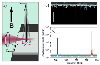
For the purposes of this work, we restrict our attention to the two fundamental flexural eigenmodes of the NWs, which oscillate along orthogonal directions and are shown schematically in Fig. 1(a). The coupling between the NW and the thermal bath results in a Langevin force equally driving both mechanical modes. Fig. 1(c) shows a calibrated power spectral density (PSD) of the NW displacement noise, where the two resonance peaks correspond to the two orthogonally polarized modes. Such a measurement shows the projection of the modes’ 2D thermal motion along the interferometric measurement axis , determined by the position of the NW in the optical waist (see Methods). Typical resonance frequencies range from 500 to 700 kHz with quality factors between and . For each NW, the doublet modes are completely decoupled by a frequency splitting of several hundred times the peak linewidth. In fact, it has been shown that even very small () cross-sectional or clamping asymmetries can split the modes by several linewidths Cadeddu et al. (2016). Nevertheless, the quality factors of the doublet modes differ by less than . The spring constants extracted from fits to the PSD for each flexural mode are on the order of , yielding mechanical dissipations and thermally-limited force sensitivities down to pg/s and few , respectively.
We exploit this high mechanical sensitivity to probe the magnetization of each individual magnetic tip. As in dynamic cantilever magnetometry (DCM) Rossel et al. (1996); Harris et al. (1999); Stipe et al. (2001), we can extract magnetic properties of each MnAs tip from the mechanical response of the NW to a uniform external magnetic field . In such a field, the resonance frequency of each orthogonal flexural mode () is modified by the curvature of the system’s magnetic energy with respect to rotations about its oscillation axis. The resulting frequency shift , where is the resonance frequency at , is given by
| (1) |
where is the NW’s spring constant and is its effective length Gross et al. (2016); Mehlin et al. (2018).
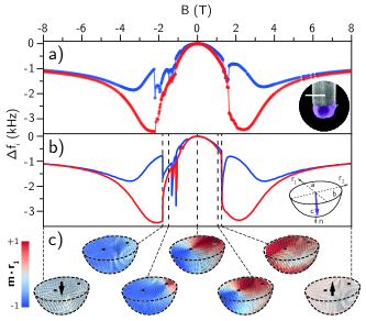
We perform measurements of on several NWs by recording the thermal displacement PSD of their doublet modes as a function of . For nearly all investigated NWs ( out of ), is negative for all applied fields (e.g. Fig. 2(a) and Fig. 3(a)). In general, negative values of correspond to a local maximum in with respect to . This behavior is consistent with being aligned along the magnetic hard axis of the MnAs tip, which should be along the NW growth-axis. Fig. 2(a) shows a particularly ideal magnetic response, in which the high-field frequency shift of both modes asymptotically approaches the same negative value. This behavior indicates a MnAs particle with a hard axis along and no preferred easy axis in the -plane.
In order to gain a deeper understanding of the DCM signal, we carry out simulations of the MnAs tips using Mumax3 Vansteenkiste et al. (2014), which employs the Landau-Lifshitz-Gilbert micromagnetic formalism using finite-difference discretization. For each value of , the simulations determine the equilibrium magnetization configuration of the MnAs particle and the corresponding values of (see Methods). The geometry of the MnAs tip is estimated by SEM and set within the simulation with respect to the two oscillation directions of the modes and the NW axis
The DCM response of the MnAs tip measured in Fig. 2(a) and shown in the inset is simulated by approximating its shape as a half ellipsoid, with dimensions given in the inset of Fig. 2(b) and its caption. The excellent agreement between the simulated and measured , both plotted in Fig. 2(b), allows us to precisely determine the direction of the magnetic hard axis. As expected, this axis is found to be nearly along : just away from and from . Furthermore, as shown in Fig. 2(c), the simulations relate a specific magnetization configuration to each value of . In this particular case, a stable vortex configuration in the easy plane is seen to enter (exit) from the edge in correspondence with the abrupt discontinuities in the eigenmodes’ frequencies around T ( T). Between these two fields, the vortex core moves from one side to the other, inducing several discontinuities in . The smoothness of the measured frequency shifts around T indicates pinning of the vortex and is well-reproduced in the simulation by the introduction of two sites of pinned magnetization (see Supplementary Information)).
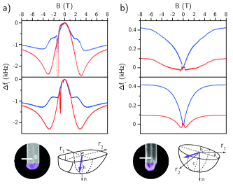
Most measured NWs present DCM curves as shown in Fig. 3(a) ( out of ). Despite the similarity of these curves to those shown in Fig. 2(a), no sharp discontinuity is observed upon sweeping down from saturation (forward applied field). Furthermore, the high-field frequency shift of both modes does not asymptotically approach the same negative value as in Fig. 2(a). Both of these effects can be explained by taking into account magnetic shape anisotropy in the MnAs tips. Despite the nearly perfect symmetry of NW’s tip, most of the crystallized MnAs droplets are asymmetric in the -plane. This asymmetry introduces an effective magnetic easy axis in the -plane. In fact, the measured shown in Fig. 3(a) are well-reproduced by a simulation that takes into a account the geometry of NW’s MnAs tip as observed by SEM. While small refinements in the microscopic geometry, which often cannot be confirmed by the SEM, affect how well the the simulation matches every detail of the measured (see Supplementary Information), the precise orientation of the hard axis and the direction of the effective shape anisotropy in the -plane sensitively determine the curves’ overall features (e.g. their high field asymptotes and shape).
In general, simulations show that shape anisotropy restricts the field range for a stable magnetic vortex to reverse applied field. In small forward applied field and in remanence, the magnetization evolves through a configuration with a net magnetic dipole in the -plane. Only upon application of a reverse field, does this configuration smoothly transform into a vortex, resulting – for NW2 – in a subtle dip in around T. At a reverse field close to T, an abrupt jump indicates the vortex’s exit and the appearance of a single-domain state, which eventually turns toward . This analysis indicates that NW’s tip – as well as the majority of the MnAs tips – present a dipole-like remanent configuration pointing in the -plane, rather than vortex-like configuration with a core pointing along , as in NW. Such remanent magnetic dipoles have been already observed by MFM in similar tips Ramlan et al. (2006); Hubmann et al. (2016).
In rare cases (1 of 12), such as the one reported for NW in Fig. 3(b), we measure mostly positive with different high-field asymptotes for each eigenmode. This behavior indicates a MnAs particle, whose hard axis points approximately in the -plane. In fact, the features of the measured in Fig. 2(b) are reproduced by a simulation considering a nearly symmetric half-ellipsoid with a hard-axis lying from and from . These data are clear evidence that crystallization of the liquid droplet can occasionally occur along a direction far off of the NW growth axis.
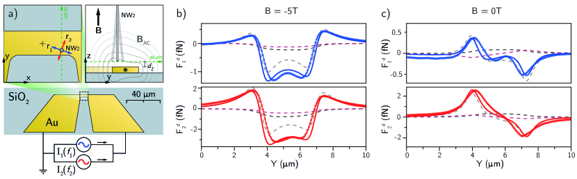
In order to test the behavior of these NWs as scanning magnetic sensors, we approach a typical one (NW2) to a current-carrying Au wire patterned on a SiO2 substrate, as described in Fig. 4(a). Once in the vicinity of the wire constriction, the NW’s two modes are excited by the Biot-Savart field resulting from an oscillating drive current , where . Single 10 -long line scans are acquired by moving the NW across the wire at the fixed tip-sample spacing nm, while both the resonant frequencies and displacement amplitudes are tracked using two phase-locked loops. The corresponding values of the force driving each mode at resonance are then calculated as (see Supplementary Information).
Using an approach similar to that used to calibrate MFM tips Lohau et al. (1999); Schendel et al. (2000); Kebe and Carl (2004), we model the force exerted by a well-known magnetic field profile on the magnetic tip by using the so-called point-probe approximation. This approximation models the complex magnetization distribution of the tip as an effective monopole moment and a dipole moment located at a distance from the tip apex (the monopole contribution compensates for the non-negligible spatial extent of the tip). The magnetic force acting on each mode is then given by . Moreover, we also consider the magnetic torque generated at the tip, which results in a torsion and/or bending of the NW depending on its orientation. Although this contribution is negligible in conventional MFM, the NW modes’ short effective length () and soft spring constant (), make the bending component of the torque responsible for an observable displacement along . We then model the total force driving each mode as , where . is set to nm from the tip (i.e. approximately at the base of the MnAs crystallite) for the best fits, while and are used as free parameters. The precise spatial dependence of the field produced by the current is calculated using the finite-element package COMSOL (see Supplementary Information).
We characterize the NW magnetic response at and . In the high field case shown in Fig. 4(b), a fit of the two driving forces is obtained with an effective dipole nearly along with a magnitude close to the dipole moment of a fully saturated tip: , where is the volume of the tip defined in the magnetometry simulation. In general, the estimation of from SEM is approximate due to the difficulty in determining the precise three-dimensional geometry and in distinguishing regions of non-magnetic material inside the tip or at its surface. The fit returns a small, but non-zero and shows a very good agreement with the measured forces sensed by the two modes. In Fig. 4(c), the same line scan is performed in absence of external field and, as expected, the observed response changes radically, since the magnetization lies mostly in the easy plane and is not completely saturated. In the fit, the effective dipole contribution is dominant and mostly orthogonal to the NW axis with . The direction of is closely related to the torque contribution making the fit particularly sensitive to the value of . Spurious electrostatic driving of the NW modes is negligible.
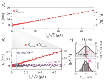
The NWs’ high force sensitivity combined with highly concentrated and strongly magnetized dipole-like tips give them an exquisite sensitivity to magnetic field gradients. In order to quantify this sensitivity, we restrict our attention to the second mode (red) of NW2, positioning it at the point of maximal response over the wire at nm and T (i.e. m on Fig 4(c)). The displacement signal is measured with a lock-in amplifier while decreasing the driving current . The sweeps plotted in Fig. 5(a) and (b) show the expected linear response as well as a wide dynamic range. In Fig. 5(b), we focus on the low-current regime, showing both the in-phase (signal+noise) and quadrature (noise) response. By simple linear regression, we find a transduction factor , where . The noise in both and is found to be Gaussian and fully ascribable to the NW’s thermal motion with variances , where is a fit to the second mode’s thermal PSD shown in Fig. 1 (c), is the resonant angular frequency of the second mode, and is the lock-in’s equivalent noise bandwidth. As shown in Fig. 5 (c) for , the mode’s thermal PSD is assumed constant around its value at resonance , due to the narrow measurement bandwidth. Therefore, the NW’s second mode has a thermally-limited displacement sensitivity of , equivalent to a force sensitivity of . Given the measured current transduction factor at the working tip-sample spacing nm, we obtain a sensitivity to current flowing through the wire of .
Such sensitivity to electrical current compares favorably to that of other microscopies capable of imaging current through Biot-Savart fields, including scanning Hall microscopy, magneto-optic microscopy, scanning SQUID microscopy, microwave impedance microscopy, and scanning nitrogen-vacancy magnetometry Kirtley (2010); Chang et al. (2017). Because of the dipole-like character of the MnAs tip, this transduction of current into displacement is dominated by the effect of the time-varying magnetic field gradient generated by the current: . Although the torque resulting from the time-varying magnetic field produces an effective force, , as seen in Figs. 4 (b) and (c), this term is typically secondary. Therefore, from COMSOL simulations of the field produced by current flowing through the wire, we find this current sensitivity to correspond to a sensitivity to magnetic field gradient of at the position of the tip’s effective point probe, i.e. nm above the surface. Having quantified the NW’s response to magnetic field gradients, we can calculate its sensitivity to other magnetic field sources, including a magnetic moment (dipole field), a superconducting vortex (monopole field), or an infinitely long and thin line of current Kirtley (2010). In particular, we expect a moment sensitivity of 54 , a flux sensitivity of 1.3 , and line-current sensitivity of . These values show the capability of magnet-tipped NWs as probes of weak magnetic field patterns and the huge potential for improvement if tips sizes and tip-sample spacings can be reduced (see Supplementary Information).
In addition to improved sensitivity, NW MFM provides other potential advantages compared to conventional MFM. First, scanning in the pendulum geometry with the NW oscillating in the plane of the sample has the characteristics of lateral MFM. This technique, which is realized with the torsional mode of a conventional cantilever, distinguishes itself from the more commonly used tapping-mode MFM in its ability to produce magnetic images devoid of spurious topography-related contrast and in a demonstrated improvement in lateral spatial resolution of up to 15% Kaidatzis and García-Martín (2013). Second, the nanometer-scale magnetic particle at the apex of the NW force sensor minimizes the size of the MFM tip, allowing for optimal spatial resolution and minimal perturbation of the investigated sample.
The prospect of increased sensitivity and resolution, combined with few restrictions on operating temperature, make NW MFM ideally suited to investigate nanometer-scale spin textures, skyrmions, superconducting and magnetic vortices, as well as ensembles of electronic or nuclear spins. Non-invasive magnetic tips may also open opportunities to study current flow in 2D materials and topological insulators. The ability of a NW sensor to map all in-plane spatial force derivatives Rossi et al. (2017); de Lépinay et al. (2017) should provide fine detail of stray field profiles above magnetic and current carrying samples, in turn providing detailed information on the underlying phenomena. Directional measurements of dissipation may also prove useful for visualizing domain walls and other regions of inhomogeneous magnetization. As shown by Grutter et al., dissipation contrast, which maps the energy transfer between the tip and the sample, strongly depends on the sample’s nanometer-scale magnetic structure Grütter et al. (1997).
Methods
Interferometric detection: The linearly polarized light emitted by a laser diode with wavelength nm is directly coupled to a polarization maintaining optical fiber, sent through the 5% transmission arm of a 95:5 fiber-optic coupler, collimated and focused on the NW by a pair of lenses. This confocal reflection microscopy setup, analogous to the one described in Högele et al. (2008), focuses light to a minimum beam waist of m (see Supplementary Information). The light incident on the NW has a power of W and is polarized along its long axis. Light scattered back by the NW interferes with light reflected by the fiber’s cleaved end, resulting in a low-finesse Fabry-Perot interferometer. A fast photo-receiver monitors variations in the intensity of reflected light, allowing for the sensitive detection of NW motion. The interferometric signal is proportional to the projection of the NW’s motion along the direction of the interference pattern’s gradient . The magnitude of this gradient at the position of the NW determines the interferometer’s transduction factor. By positioning the NW within the optical waist or changing the wavelength of the laser, it is possible to measure the motion projected along arbitrary directions. For displacement measurements presented in this work, NWs have been positioned on the optical axis in order to have (see Supplementary Information).
Numerical simulations: Micromagnetic simulations are carried out with Mumax3. We set the saturation magnetization T, the exchange stiffness constant pJ/m, and the magnetocrystalline anisotropy in correspondence with the values reported for MnAs in the literature De Blois and Rodbell (1963); Engel-Herbert et al. (2006). We model the geometry of each MnAs magnetic tip based on observations made in a SEM. Space is discretized into cubic mesh elements, which are nm on a side, which corresponds to the dipolar exchange length of the material . The validity of this discretization is confirmed by comparing the results of a few representative simulations with simulations using much smaller mesh sizes. Mumax3 determines the equilibrium magnetization configuration for each external field value by numerically solving the Landau-Lifshitz-Gilbert equation. Since the microscopic processes in a MnAs tip are expected to be much faster than the NW resonance frequencies, the magnetization of the tip is assumed to be in its equilibrium orientation throughout the cantilever oscillation. The calculation also yields the total magnetic energy corresponding to each configuration. In order to simulate , we numerically calculate the second derivatives of with respect to found in (1). At each field, we calculate at the equilibrium angles and at small deviations from equilibrium . For small , the second derivative can be approximated by a finite difference: . By setting , , and to their measured values, we then arrive at the corresponding to each magnetization configuration in the numerically calculated field dependence.
Supplementary Information
Supplementary information is available for download at RossiSupp.pdf. This file includes sections discussing: the optical setup for NW motion detection; displacement calibration and force estimation; micromagnetic simulations of NW magnetometry; simulated profile; sensitivity to different types of magnetic field sources.
Acknowledgements
We thank Sascha Martin and his team in the machine shop of the Physics Department at the University of Basel for help building the measurement system. We thank Lorenzo Ceccarelli for help with magnetic field simulations and Prof. Ilaria Zardo for suggesting the collabroation. We acknowledge the support of the Kanton Aargau, the ERC through Starting Grant NWScan (Grant No. 334767), the SNF under Grant No. 200020-178863, the Swiss Nanoscience Institute, the NCCR Quantum Science and Technology (QSIT), and the DFG via project GR1640/5-2 in SPP 153.
References
- Schmid et al. (2010) I. Schmid, M. A. Marioni, P. Kappenberger, S. Romer, M. Parlinska-Wojtan, H. J. Hug, O. Hellwig, M. J. Carey, and E. E. Fullerton, Phys. Rev. Lett. 105, 197201 (2010).
- Poggio (2013) M. Poggio, Nat. Nanotechnol. 8, 482 (2013).
- Lisunova et al. (2013) Y. Lisunova, J. Heidler, I. Levkivskyi, I. Gaponenko, A. Weber, C. Caillier, L. J. Heyderman, M. Kläui, and P. Paruch, Nanotechnology 24, 105705 (2013).
- Rondin et al. (2013) L. Rondin, J.-P. Tetienne, S. Rohart, A. Thiaville, T. Hingant, P. Spinicelli, J.-F. Roch, and V. Jacques, Nat. Commun. 4, 2279 (2013).
- Tetienne et al. (2014) J.-P. Tetienne, T. Hingant, J.-V. Kim, L. H. Diez, J.-P. Adam, K. Garcia, J.-F. Roch, S. Rohart, A. Thiaville, D. Ravelosona, and V. Jacques, Science 344, 1366 (2014).
- Tetienne et al. (2015) J.-P. Tetienne, T. Hingant, L. J. Martínez, S. Rohart, A. Thiaville, L. H. Diez, K. Garcia, J.-P. Adam, J.-V. Kim, J.-F. Roch, I. M. Miron, G. Gaudin, L. Vila, B. Ocker, D. Ravelosona, and V. Jacques, Nat. Commun. 6, 6733 (2015).
- Dovzhenko et al. (2016) Y. Dovzhenko, F. Casola, S. Schlotter, T. X. Zhou, F. Büttner, R. L. Walsworth, G. S. D. Beach, and A. Yacoby, arXiv:1611.00673 (2016).
- Thiel et al. (2016) L. Thiel, D. Rohner, M. Ganzhorn, P. Appel, E. Neu, B. Müller, R. Kleiner, D. Koelle, and P. Maletinsky, Nat. Nanotechnol. 11, 677 (2016).
- Pelliccione et al. (2016) M. Pelliccione, A. Jenkins, P. Ovartchaiyapong, C. Reetz, E. Emmanouilidou, N. Ni, and A. C. Bleszynski Jayich, Nat. Nanotechnol. 11, 700 (2016).
- Tetienne et al. (2017) J.-P. Tetienne, N. Dontschuk, D. A. Broadway, A. Stacey, D. A. Simpson, and L. C. L. Hollenberg, Sci. Adv. 3, e1602429 (2017).
- Rugar et al. (2015) D. Rugar, H. J. Mamin, M. H. Sherwood, M. Kim, C. T. Rettner, K. Ohno, and D. D. Awschalom, Nat. Nanotechnol. 10, 120 (2015).
- Häberle et al. (2015) T. Häberle, D. Schmid-Lorch, F. Reinhard, and J. Wrachtrup, Nat Nano 10, 125 (2015).
- Degen et al. (2009) C. L. Degen, M. Poggio, H. J. Mamin, C. T. Rettner, and D. Rugar, Proc. Natl. Acad. Sci. U.S.A. 106, 1313 (2009).
- Poggio and Degen (2010) M. Poggio and C. L. Degen, Nanotechnology 21, 342001 (2010), 00041.
- Gloppe et al. (2014) A. Gloppe, P. Verlot, E. Dupont-Ferrier, A. Siria, P. Poncharal, G. Bachelier, P. Vincent, and O. Arcizet, Nat. Nanotechnol. 9, 920 (2014).
- Rossi et al. (2017) N. Rossi, F. R. Braakman, D. Cadeddu, D. Vasyukov, G. Tütüncüoglu, A. Fontcuberta i Morral, and M. Poggio, Nat. Nanotechnol. 12, 150 (2017).
- de Lépinay et al. (2017) L. M. de Lépinay, B. Pigeau, B. Besga, P. Vincent, P. Poncharal, and O. Arcizet, Nat. Nanotechnol. 12, 156 (2017).
- Siria and Niguès (2017) A. Siria and A. Niguès, Sci. Rep. 7, 11595 (2017).
- Nichol et al. (2012) J. M. Nichol, E. R. Hemesath, L. J. Lauhon, and R. Budakian, Phys. Rev. B 85, 054414 (2012).
- Nichol et al. (2013) J. M. Nichol, T. R. Naibert, E. R. Hemesath, L. J. Lauhon, and R. Budakian, Phys. Rev. X 3, 031016 (2013).
- Colombo et al. (2008) C. Colombo, D. Spirkoska, M. Frimmer, G. Abstreiter, and A. Fontcuberta i Morral, Phys. Rev. B 77, 155326 (2008).
- Hubmann et al. (2016) J. Hubmann, B. Bauer, H. S. Körner, S. Furthmeier, M. Buchner, G. Bayreuther, F. Dirnberger, D. Schuh, C. H. Back, J. Zweck, E. Reiger, and D. Bougeard, Nano Lett. 16, 900 (2016).
- Bean and Rodbell (1962) C. P. Bean and D. S. Rodbell, Phys. Rev. 126, 104 (1962).
- De Blois and Rodbell (1963) R. W. De Blois and D. S. Rodbell, Phys. Rev. 130, 1347 (1963).
- Nichol et al. (2008) J. M. Nichol, E. R. Hemesath, L. J. Lauhon, and R. Budakian, Appl. Phys. Lett. 93, 193110 (2008).
- Cadeddu et al. (2016) D. Cadeddu, F. R. Braakman, G. Tütüncüoglu, F. Matteini, D. Rüffer, A. Fontcuberta i Morral, and M. Poggio, Nano Lett. 16, 926 (2016).
- Rossel et al. (1996) C. Rossel, P. Bauer, D. Zech, J. Hofer, M. Willemin, and H. Keller, J. Appl. Phys. 79, 8166 (1996).
- Harris et al. (1999) J. G. E. Harris, D. D. Awschalom, F. Matsukura, H. Ohno, K. D. Maranowski, and A. C. Gossard, Appl. Phys. Lett. 75, 1140 (1999).
- Stipe et al. (2001) B. C. Stipe, H. J. Mamin, T. D. Stowe, T. W. Kenny, and D. Rugar, Phys. Rev. Lett. 86, 2874 (2001).
- Gross et al. (2016) B. Gross, D. P. Weber, D. Rüffer, A. Buchter, F. Heimbach, A. Fontcuberta i Morral, D. Grundler, and M. Poggio, Phys. Rev. B 93, 064409 (2016).
- Mehlin et al. (2018) A. Mehlin, B. Gross, M. Wyss, T. Schefer, G. Tütüncüoglu, F. Heimbach, A. Fontcuberta i Morral, D. Grundler, and M. Poggio, Phys. Rev. B 97, 134422 (2018).
- Vansteenkiste et al. (2014) A. Vansteenkiste, J. Leliaert, M. Dvornik, M. Helsen, F. Garcia-Sanchez, and B. Van Waeyenberge, AIP Adv. 4, 107133 (2014).
- Ramlan et al. (2006) D. G. Ramlan, S. J. May, J.-G. Zheng, J. E. Allen, B. W. Wessels, and L. J. Lauhon, Nano Lett. 6, 50 (2006).
- Lohau et al. (1999) J. Lohau, S. Kirsch, A. Carl, G. Dumpich, and E. F. Wassermann, J. Appl. Phys. 86, 3410 (1999).
- Schendel et al. (2000) P. J. A. v. Schendel, H. J. Hug, B. Stiefel, S. Martin, and H.-J. Güntherodt, J. Appl. Phys. 88, 435 (2000).
- Kebe and Carl (2004) T. Kebe and A. Carl, J. Appl. Phys. 95, 775 (2004).
- Kirtley (2010) J. R. Kirtley, Rep. Prog. Phys. 73, 126501 (2010).
- Chang et al. (2017) K. Chang, A. Eichler, J. Rhensius, L. Lorenzelli, and C. L. Degen, Nano Lett. 17, 2367 (2017).
- Kaidatzis and García-Martín (2013) A. Kaidatzis and J. M. García-Martín, Nanotechnology 24, 165704 (2013).
- Grütter et al. (1997) P. Grütter, Y. Liu, P. LeBlanc, and U. Dürig, Appl. Phys. Lett. 71, 279 (1997).
- Högele et al. (2008) A. Högele, S. Seidl, M. Kroner, K. Karrai, C. Schulhauser, O. Sqalli, J. Scrimgeour, and R. J. Warburton, Rev. Sci. Inst. 79, 023709 (2008).
- Engel-Herbert et al. (2006) R. Engel-Herbert, T. Hesjedal, D. M. Schaadt, L. Däweritz, and K. H. Ploog, Appl. Phys. Lett. (2006).