Encapsulation Narrows Excitonic Homogeneous Linewidth of Exfoliated \ceMoSe2 Monolayer
Abstract
The excitonic homogeneous linewidth of an exfoliated monolayer \ceMoSe2 encapsulated in hexagonal boron nitride is directly measured using multidimensional coherent spectroscopy with micron spatial resolution. The linewidth is 0.26 0.02 meV, corresponding to a dephasing time 2.5 ps, which is almost half the narrowest reported values for non-encapsulated \ceMoSe2 flakes. We attribute the narrowed linewidth to Coulomb screening by the encapsulated material and suppression of non-radiative processes. Through direct measurements of encapsulated and non-encapsulated monolayers, we confirm that encapsulation reduces the sample inhomogeneity. However, linewidths measured using photoluminescence and linear absorption remain dominated by inhomogeneity, and these linewidths are roughly 5 times larger than the homogeneous linewidth in even the highest-quality encapsulated materials. The homogeneous linewidth of non-encapsulated monolayers is very sensitive to temperature cycling, whereas encapsulated samples are not modified by temperature cycling. The nonlinear signal intensity of non-encapsulated monolayers is degraded by high-power optical excitation, whereas encapsulated samples are very resilient to optical excitation with optical powers up to the point of completely bleaching the exciton.
keywords:
Transition metal dichalcogenides, encapsulated monolayer, homogeneous linewidth, radiative lifetime, multidimensional coherent spectroscopyThese authors contributed equally. \altaffiliationThese authors contributed equally. University of Michigan] Department of Physics, University of Michigan, Ann Arbor, MI 48109-1040, USA \abbreviationsMDCS, TMDC, FWM, OBE
Monolayer van der Waals crystals are a class of materials with widely varying properties and the potential to transform future electronics and optoelectronics 1, 2, 3. These atomically thin layered materials can be stacked into heterostructures with new functionalities 4. A subset of these materials are the semiconducting monolayer transition metal dichalcogenides (TMDCs), which have a direct band gap that makes their electronic transitions optically accessible and thus useful for optoelectronic applications 5, 6, 7, 8. The low dimensionality resulting from confinement to a monolayer also means monolayer TMDCs have very strong many-body interactions that result in 100x larger binding energy of excitons than more conventional III-V semiconductors, such as gallium arsenide. Excitons thus dominate the optical response of semiconductor TMDCs and remain strongly bound at room temperature. The low dimensionality also means excitations in these materials are very sensitive to the external dielectric environment through both screening and introduction of defects.
Encapsulation of monolayer van der Waals crystals in hexagonal boron nitride (hBN) enhances carrier mobility 9, 10 and significantly improves the monolayer resistance to photodegradation 11. Most notably hBN encapsulation has been shown to greatly reduce the photoluminescence linewidth of \ceMoSe2, \ceMoS2, \ceWSe2, and \ceWS2 12, 13, 14.
Narrowing of the photoluminescence linewidth of a TMDC monolayer has been taken as an indicator that encapsulation passivates the monolayer and minimizes inhomogeneity resulting from trapped states and defects. However, narrowing of the photoluminescence linewidth can also result from a change in the radiative linewidth of the exciton, which scales with the substrate index. The substrate can further affect the linewidth through its effect on pure dephasing resulting from interactions of the exciton with photons, phonons, and other collective modes. So while it is impressive that encapsulated TMDC photoluminescence linewidths approach the homogeneous limits measured in similar monolayers on different substrates, linear techniques cannot disentangle the linewidth contributions from inhomogeneous broadening, non-radiative processes, and radiative decay. Here we show that encapsulation narrows both the homogeneous and inhomogeneous linewidths such that the inhomogeneous linewidth still dominates. We discuss how our results imply that hBN-encapsulation of monolayer TMDC samples minimizes defects and static doping that result in both long- and short-range disorder. Along with the static lineshape differences, we measure significant permanent modification of the homogeneous linewidth of non-encapsulated samples resulting from temperature cycling and exposure to weak radiation. In contrast, encapsulated samples are very robust to numerous temperature cycles and high radiation exposure.
To directly measure homogeneous linewidths and distinguish the dephasing and decay processes, it is necessary to use nonlinear spectroscopy techniques. Homogeneous linewidths of exciton resonances in bare monolayer TMDC samples have been measured using four-wave-mixing (FWM) based techniques 15, 16, 17. Multidimensional coherent spectroscopy (MDCS) was employed by Moody et al. to measure the homogeneous linewidth of \ceWSe2 grown by chemical vapor deposition (CVD) 15 and to identify higher order correlated states in a large exfoliated \ceMoSe2 flake 18. MDCS is useful for its ability to unambiguously separate homogeneous and inhomogeneous broadening of exciton linewidths. However, as is typical of most MDCS techniques, this MDCS implementation uses a non-collinear geometry to isolate the signal from the excitation beams, and it is therefor limited by having a relatively large spot size (30 µm). The large spot size requires large samples, and large CVD grown samples are known to show worse quality and mid-gap defects as compared to exfoliated samples 19, 20. Jakubczyk et al. used three-pulse FWM microspectroscopy to measure exfoliated \ceMoSe2. This FWM technique provides similar information to MDCS for lineshapes without inhomogeneous dephasing rates 21. The authors demonstrate tremendous variability of the exciton transition energy (greater than 10 meV) and dephasing time (between 0.5 and 1.5 ps) over the single large exfoliated flake 16.
Here we use MDCS in conjunction with linear reflectance spectroscopy to compare the neutral exciton linewidths of fully hBN-encapsulated and non-encapsulated exfoliated \ceMoSe2 monolayer samples. Prototypical samples, including heterostructures consisting of exfoliated monolayer materials, are often small. The samples measured here are all between 5 and 8 µm wide. Example images of two of these samples are presented in Fig. 1(a). The small sample size demands the use of collinear techniques for all optical measurements. For linear spectroscopies including photoluminescence and linear absorption, the excitation source is easily distinguished from the sample response. For MDCS it is necessary to distinguish a specific third order response from the excitation sources, linear response, and all other nonlinear responses. The conventional method for isolating the MDCS signal is with k-vector selection 22, but this method is not congruent with having a tight focus. We have developed a collinear MDCS that has enabled measurements of samples within a diffraction limited spot 23 based on frequency modulation 24. For these MDCS measurements we use a spot size of 2 µm.
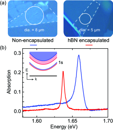
We compare four high quality samples: two monolayer \ceMoSe2 mounted on sapphire substrates and two hBN encapuslated monolayer \ceMoSe2 also mounted on sapphire. The encapsulated monolayers are on a bottom layer of hBN that is approximately 120 nm and a top layer that is approximately 20 nm, measured with atomic force microscopy. We measure encapsulated samples that are of a similar high-quality to others reported in the literature 14, 25, 26, evidenced by the comparable linewidths measured with linear techniques. We plot the linear absorption in Fig. 1(b) in which the exciton of the encapsulated sample has a half width at half maximum (HWHM) linewidth of 2.19 meV. The photoluminescence of this sample has a HWHM linewidth of 1.49 meV. The significant decrease of the total absorption of light by the encapsulated sample is an additional indicator that encapsulation decreases the non-radiative decay processes that contribute to incoherent absorption. We also see that the transition energies of excitons in the two samples differ by about 20 meV. This difference is primarily due to the significant decrease of both the band gap and partially compensating exciton binding energy by encapsulating the monolayer in a high index material 27, 28. We depict these changes in the inset of Fig. 1(b). With measure the effects of encapsulation on both the inhomogeneous and homogeneous exciton linewidths using MDCS.
In Fig. 2(a) we plot characteristic multidimensional coherent spectra at low temperature using a rephasing pulse sequence. To generate these plots we measure the phase-resolved evolution of an induced nonlinear response as a function of the evolution of a phase-resolved linear response. We measure these responses using a sequence of four pulses in the time domain having relative delays (\texttau between the first two pulses, T between the second and third pulse, and t between the last two pulses) that are referenced to a co-propagating continuous-wave laser. Fourier transforming the response with respect to two of the pulse delays yields spectra with two dimensions that correlates absorption () and emission () energies of the sample coherences 22, 23. The evolution of the absorption in this type of MDCS, called a rephasing measurement, has the opposite sign to the emission, so these frequencies are negative. Since a single resonance absorbs and emits at the same energy, a distribution of resonances will all fall along the diagonal where . Thus the lineshape of the diagonal slice plotted on the left in Fig. 2(b) roughly corresponds to inhomogenous distributions of exciton resonances in the non-encapsulated (blue) and hBN-encapsulated (red) samples. The lineshape of the cross-diagonal slice plotted on the right roughly corresponds to the homogeneous linewidth of those exciton resonances. For a more detailed description of the MDCS experiment, see the Supporting Information.
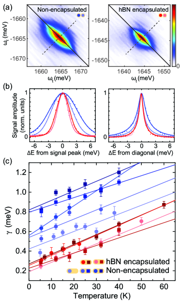
Though the cross-diagonal linewidth roughly corresponds to the homogeneous linewidth, the lineshape depends on the inhomogeneous distribution. For low inhomogeneity the cross-diagonal lineshape is a Lorentzian. However, in the limit of high inhomogeneity the lineshape is the square root of a Lorentzian 30. Ignoring inhomogeneous broadening and using the wrong fit function when determining a sample’s homogeneous linewidth (or dephasing times in photon echo FWM experiments) can thus significantly skew the measurement, up to a factor of . For inhomogeneous linewidths that are comparable to the homogeneous linewidth, as is the case in these samples, it is essential to simultaneously fit the codependent diagonal and cross-diagonal slices. Here we fit the entire two-dimensional spectrum using an analytical solution to the optical Bloch equations (OBEs) derived by Bell et al. 29.
We measure the homogeneous linewidth as a function of beam power and sample temperature. Exciton-exciton interactions are density dependent, and so we measure the density dependence of the linewidth to determine their contribution. We increase the power of all three excitation beams equally, and determine the linewidth scaling as a function of the excitation density of a single beam. We estimate that the linewidth linearly broadens with a slope of meV cm2, shown in the Supporting Information. We measure this linear dependence up to an excitation density of 1012 cm-2. For each sample temperature, measured between 5 and 80 K, we extrapolate the power dependence of the linewidth to zero power and plot that as . Exciton-phonon scattering can be suppressed by lowering the sample temperature to nearly 0 K. At low temperatures the phonon broadening is due to acoustic phonons, which has a linear dependence on temperature. In Fig. 2(c) we plot as a function of temperature for the four different samples. The non-encapsulated samples are indicated in blue. The circle data points correspond to a first set of measurements on a sample, where the linewidths are first measured at 5.3 K and the temperature is increased. The square data points correspond to measurements made after a temperature cycle defined by warming the sample up to room temperature and cooling it back down to again start the measurement set at 5.3 K. It is evident from this data that the linewidth of the non-encapsulated monolayer is very sample dependent, which confirms results by Jakubczyk et al. 16, 17. We further find significant broadening of the exciton linewidth of non-encapsulated samples with a single temperature cycle. By measuring many points on the sample, we confirm that the broadening effect is not the result of a positioning error. We rather suggest that the broadening is likely due to deposition of molecules such as water on the sample surface. Whether the change results from surface molecules or substrate strain, we demonstrate that the homogeneous linewidth is a sensitive indicator of a change in the sample environment. The hBN-encapsulated monolayer samples are indicated in red. The sample variance is very small, and there is no measurable broadening due to temperature cycling in these samples. This consistency is evidence that defect scattering is minimal in encapsulated samples. The durability of the monolayer with temperature cycling is an important confirmation that experiments on encapsulated samples will be consistent and reproducible.
From the temperature dependence we measure a linewidth broadening of 0.010 0.001 meV/K by averaging the hBN encapsulated sample linewidths. This exciton-acoustic phonon interaction is similar to those measured for the non-encapsulated samples confirming previous results 16, similar to the interaction in ZnSe (slope = 8 µeV/K) 31, and approximately double the interaction GaAs quantum wells (slope = 5 µeV/K) 32. The most homogeneous sample we measure has an extrapolated zero temperature and zero power linewidth of meV, and the average linewidth for the encapsulated samples is meV. This average linewidth corresponds to a dephasing time ps. Since the sample variance of the non-encapsulated samples likely results from surface molecules and substrate effects, the broadest linewidths are dominated by non-radiative decay and pure dephasing processes. Though it is important to note that measurements of the homogeneous linewidth can only identify an upper bound of the radiative linewidth, we identify the lowest measured linewidth for the non-encapsulated samples as the nearest to the radiatively limited linewidth for these samples. For this non-encapsulated sample meV, which corresponds to ps. This latter value is in agreement with previous determinations of the longest times measured in \ceMoSe2 using FWM 16 and time-resolved photoluminescence 33. The average linewidth for non-encapsulated samples is meV.
We attribute the homogeneous linewidth differences between the hBN encapsulated monolayer and the monolayer directly on sapphire to a combination of factors. The decreased defects and static doping in the encapsulated samples of course minimize the variance. One would expect additional narrowing of the homogeneous linewidth of the encapsulated sample due to the difference in the dielectric environments. The radiative linewidth should scale with the substrate refractive index: 34. For a radiatively-limited homogeneous linewidth, one would thus expect an hBN encapsulated sample to have a times narrower linewidth than an equivalent sample on sapphire.
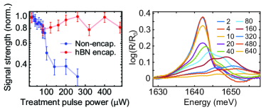
Finally we compare photodegradation of low temperature samples resulting from excitation by resonant pulses. We treat samples by irradiating them with laser light for one minute at the given treatment beam power. The pulsed light is focused to a 2 µm spot and has a repetition frequency of 76 MHz. After each treatment we turn off the treatment beam and measure a multidimensional spectrum with low power, 1 µW/beam, pulses. In Fig. 3 we plot the MDCS signal strength as a function of treatment pulse power. We find that the non-encapsulated samples exhibit lasting damage by beams having powers greater than 45 µW. Measured homogeneous linewidths vary significantly between treatments and scans. The encapsulated samples, however, are resilient up to powers that fully saturate the exciton and have a consistent homogeneous linewidth. We demonstrate saturation of the exciton in an encapsulated sample with single pulse reflectance, similar to an experiment recently presented on non-encapsulated samples 26. We plot reflectance measured with beams having powers between 2 and 640 µW, a range over which the sample is not damaged. Reflectance at the exciton resonance of the encapsulated sample with a beam having a power of 640 µW is saturated. This type of measurement would not be reliable in non-encapsulated \ceMoSe2.
In summary, we have measured a significant improvement in sample consistency and stability by encapsulating monolayer \ceMoSe2 in hBN. In agreement with previous studies, we find that encapsulated samples have narrower inhomogeneous linewidths than non-encapsulated samples. However, we also find that the excitonic homogeneous linewidth is still significantly narrower than the total linewidth. The measurements indicates that inhomogeneity must still be considered in low temperature studies, and the homogeneous linewidth is the upper bound for the radiative linewidth in these samples. Beyond the intrinsic changes to the monolayer by hBN-encapsulation, we demonstrate that encapsulated samples are more robust to high optical excitations. This resilience is essential for lasing applications and ensuring experiments are reproducible.
EWM, HGR, and STC acknowledge the support by the National Science Foundation (NSF) under Grant No. 1622768 and the MCubed Program at the University of Michigan. JH, EP and HD acknowledge the support by the Army Research Office under Award W911NF-17-1-0312 (MURI). MHW acknowledges the support by the University of Michigan Undergraduate Research Opportunity Program.
Detailed schematic and description of the MDCS experiment and experimental procedures can be found in the Supporting Information:
References
- Radisavljevic et al. 2011 Radisavljevic, B.; Radenovic, A.; Brivio, J.; Giacometti, V.; Kis, A. Single-layer MoS2 transistors. Nature Nanotechnology 2011, 6, 147 EP –
- Baugher et al. 2013 Baugher, B. W. H.; Churchill, H. O. H.; Yang, Y.; Jarillo-Herrero, P. Intrinsic Electronic Transport Properties of High-Quality Monolayer and Bilayer MoS2. Nano Letters 2013, 13, 4212–4216, PMID: 23930826
- Zhang et al. 2012 Zhang, Y.; Ye, J.; Matsuhashi, Y.; Iwasa, Y. Ambipolar MoS2 Thin Flake Transistors. Nano Letters 2012, 12, 1136–1140, PMID: 22276648
- Novoselov et al. 2016 Novoselov, K. S.; Mishchenko, A.; Carvalho, A.; Castro Neto, A. H. 2D materials and van der Waals heterostructures. Science 2016, 353
- Ye et al. 2015 Ye, Y.; Wong, Z. J.; Lu, X.; Ni, X.; Zhu, H.; Chen, X.; Wang, Y.; Zhang, X. Monolayer excitonic laser. Nature Photonics 2015, 9, 733 EP –
- Wu et al. 2015 Wu, S.; Buckley, S.; Schaibley, J. R.; Feng, L.; Yan, J.; Mandrus, D. G.; Hatami, F.; Yao, W.; Vuckovic, J.; Majumdar, A.; Xu, X. Monolayer semiconductor nanocavity lasers with ultralow thresholds. Nature 2015, 520, 69 EP –
- Salehzadeh et al. 2015 Salehzadeh, O.; Djavid, M.; Tran, N. H.; Shih, I.; Mi, Z. Optically Pumped Two-Dimensional MoS2 Lasers Operating at Room-Temperature. Nano Letters 2015, 15, 5302–5306
- Pospischil et al. 2014 Pospischil, A.; Furchi, M. M.; Mueller, T. Solar-energy conversion and light emission in an atomic monolayer p-n diode. Nature Nanotechnology 2014, 9, 257 EP –
- Dean et al. 2010 Dean, C. R.; Young, A. F.; Meric, I.; Lee, C.; Wang, L.; Sorgenfrei, S.; Watanabe, K.; Taniguchi, T.; Kim, P.; Shepard, K. L.; Hone, J. Boron nitride substrates for high-quality graphene electronics. Nature Nanotechnology 2010, 5, 722 EP –
- Cui et al. 2015 Cui, X. et al. Multi-terminal transport measurements of MoS2 using a van der Waals heterostructure device platform. Nature Nanotechnology 2015, 10, 534 EP –
- Ahn et al. 2016 Ahn, S.; Kim, G.; Nayak, P. K.; Yoon, S. I.; Lim, H.; Shin, H.-J.; Shin, H. S. Prevention of Transition Metal Dichalcogenide Photodegradation by Encapsulation with h-BN Layers. ACS Nano 2016, 10, 8973–8979
- Cadiz et al. 2017 Cadiz, F. et al. Excitonic Linewidth Approaching the Homogeneous Limit in -Based van der Waals Heterostructures. Phys. Rev. X 2017, 7, 021026
- Ajayi et al. 2017 Ajayi, O. A.; Ardelean, J. V.; Shepard, G. D.; Wang, J.; Antony, A.; Taniguchi, T.; Watanabe, K.; Heinz, T. F.; Strauf, S.; Zhu, X.-Y.; Hone, J. C. Approaching the intrinsic photoluminescence linewidth in transition metal dichalcogenide monolayers. 2D Materials 2017, 4, 031011
- Wierzbowski et al. 2017 Wierzbowski, J.; Klein, J.; Sigger, F.; Straubinger, C.; Kremser, M.; Taniguchi, T.; Watanabe, K.; Wurstbauer, U.; Holleitner, A. W.; Kaniber, M.; Müller, K.; Finley, J. J. Direct exciton emission from atomically thin transition metal dichalcogenide heterostructures near the lifetime limit. Scientific Reports 2017, 7, 12383
- Moody et al. 2015 Moody, G.; Kavir Dass, C.; Hao, K.; Chen, C.-H.; Li, L.-J.; Singh, A.; Tran, K.; Clark, G.; Xu, X.; Berghäuser, G.; Malic, E.; Knorr, A.; Li, X. Intrinsic homogeneous linewidth and broadening mechanisms of excitons in monolayer transition metal dichalcogenides. Nature Communications 2015, 6, 8315 EP –
- Jakubczyk et al. 2016 Jakubczyk, T.; Delmonte, V.; Koperski, M.; Nogajewski, K.; Faugeras, C.; Langbein, W.; Potemski, M.; Kasprzak, J. Radiatively Limited Dephasing and Exciton Dynamics in MoSe2 Monolayers Revealed with Four-Wave Mixing Microscopy. Nano Letters 2016, 16, 5333–5339
- Jakubczyk et al. 2018 Jakubczyk, T.; Nogajewski, K.; Molas, M. R.; Bartos, M.; Langbein, W.; Potemski, M.; Kasprzak, J. Impact of environment on dynamics of exciton complexes in a WS 2 monolayer. 2D Materials 2018, 5, 031007
- Hao et al. 2017 Hao, K.; Specht, J. F.; Nagler, P.; Xu, L.; Tran, K.; Singh, A.; Dass, C. K.; Schüller, C.; Korn, T.; Richter, M.; Knorr, A.; Li, X.; Moody, G. Neutral and charged inter-valley biexcitons in monolayer MoSe2. Nature Communications 2017, 8, 15552 EP –
- Choi et al. 2017 Choi, W.; Choudhary, N.; Han, G. H.; Park, J.; Akinwande, D.; Lee, Y. H. Recent development of two-dimensional transition metal dichalcogenides and their applications. Materials Today 2017, 20, 116 – 130
- Chen et al. 2017 Chen, K.; Ghosh, R.; Meng, X.; Roy, A.; Kim, J.-S.; He, F.; Mason, S. C.; Xu, X.; Lin, J.-F.; Akinwande, D.; Banerjee, S. K.; Wang, Y. Experimental evidence of exciton capture by mid-gap defects in CVD grown monolayer MoSe2. npj 2D Materials and Applications 2017, 1, 15
- Spivey and Cundiff 2007 Spivey, A. G. V.; Cundiff, S. T. Inhomogeneous dephasing of heavy-hole and light-hole exciton coherences in GaAs quantum wells. J. Opt. Soc. Am. B 2007, 24, 664–670
- Cundiff and Mukamel 2013 Cundiff, S. T.; Mukamel, S. Optical multidimensional coherent spectroscopy. Phys. Today 2013, 66, 44
- Martin and Cundiff 2018 Martin, E. W.; Cundiff, S. T. Inducing coherent quantum dot interactions. Phys. Rev. B 2018, 97, 081301
- Tekavec et al. 2007 Tekavec, P. F.; Lott, G. A.; Marcus, A. H. Fluorescence-detected two-dimensional electronic coherence spectroscopy by acousto-optic phase modulation. The Journal of Chemical Physics 2007, 127, 214307
- Back et al. 2018 Back, P.; Zeytinoglu, S.; Ijaz, A.; Kroner, M.; Imamoğlu, A. Realization of an Electrically Tunable Narrow-Bandwidth Atomically Thin Mirror Using Monolayer . Phys. Rev. Lett. 2018, 120, 037401
- Scuri et al. 2018 Scuri, G.; Zhou, Y.; High, A. A.; Wild, D. S.; Shu, C.; De Greve, K.; Jauregui, L. A.; Taniguchi, T.; Watanabe, K.; Kim, P.; Lukin, M. D.; Park, H. Large Excitonic Reflectivity of Monolayer Encapsulated in Hexagonal Boron Nitride. Phys. Rev. Lett. 2018, 120, 037402
- Cadiz et al. 2017 Cadiz, F. et al. Excitonic Linewidth Approaching the Homogeneous Limit in -Based van der Waals Heterostructures. Phys. Rev. X 2017, 7, 021026
- Stier et al. 2016 Stier, A. V.; Wilson, N. P.; Clark, G.; Xu, X.; Crooker, S. A. Probing the Influence of Dielectric Environment on Excitons in Monolayer WSe2: Insight from High Magnetic Fields. Nano Letters 2016, 16, 7054–7060, PMID: 27718588
- Bell et al. 2015 Bell, J. D.; Conrad, R.; Siemens, M. E. Analytical calculation of two-dimensional spectra. Opt. Lett. 2015, 40, 1157–1160
- Siemens et al. 2010 Siemens, M. E.; Moody, G.; Li, H.; Bristow, A. D.; Cundiff, S. T. Resonance lineshapes in two-dimensional Fourier transform spectroscopy. Opt. Express 2010, 18, 17699–17708
- Wagner et al. 1997 Wagner, H. P.; Schätz, A.; Maier, R.; Langbein, W.; Hvam, J. M. Coherent optical nonlinearities and phase relaxation of quasi-three-dimensional and quasi-two-dimensional excitons in structures. Phys. Rev. B 1997, 56, 12581–12588
- Schultheis et al. 1986 Schultheis, L.; Honold, A.; Kuhl, J.; Köhler, K.; Tu, C. W. Optical dephasing of homogeneously broadened two-dimensional exciton transitions in GaAs quantum wells. Phys. Rev. B 1986, 34, 9027–9030
- Robert et al. 2016 Robert, C.; Lagarde, D.; Cadiz, F.; Wang, G.; Lassagne, B.; Amand, T.; Balocchi, A.; Renucci, P.; Tongay, S.; Urbaszek, B.; Marie, X. Exciton radiative lifetime in transition metal dichalcogenide monolayers. Phys. Rev. B 2016, 93, 205423
- Selig et al. 2016 Selig, M.; Berghäuser, G.; Raja, A.; Nagler, P.; Schüller, C.; Heinz, T. F.; Korn, T.; Chernikov, A.; Malic, E.; Knorr, A. Excitonic linewidth and coherence lifetime in monolayer transition metal dichalcogenides. Nature Communications 2016, 7, 13279 EP –