High-Density Qubit Wiring: Pin-Chip Bonding for Fully Vertical Interconnects
Abstract
Large-scale quantum computers with more than qubits will likely be built within the next decade. Trapped ions, semiconductor devices, and superconducting qubits among other physical implementations are still confined in the realm of medium-scale quantum integration ( qubits); however, they show promise toward large-scale quantum integration. Building large-scale quantum processing units will require truly scalable control and measurement classical coprocessors as well as suitable wiring methods. In this blue paper, we introduce a fully vertical interconnect that will make it possible to address superconducting qubits fabricated on a single silicon or sapphire chip: Pin-chip bonding. This method permits signal transmission from DC to , both at room temperature and at cryogenic temperatures down to . At temperatures below , the on-chip wiring contact resistance is close to zero and all signal lines are in the superconducting state. High-density wiring is achieved by means of a fully vertical interconnect that interfaces the qubit array with a network of rectangular coaxial ribbon cables. Pin-chip bonding is fully compatible with classical high-density test board applications as well as with other qubit implementations.
I INTRODUCTION
Practical quantum computers are closer to reality than ever before Neill et al. (2018). Among a variety of physical implementations Ladd et al. (2010), those based on superconducting quantum circuits Clarke and Wilhelm (2008); Wendin (2017) show promise for the realization of medium-scale quantum computers comprising on the order of qubits Knight (2017); Giles and Knight (2018). It is expected that these computers will allow us to tackle problems with real-world applications, such as the quantum simulation of chemical reactions, quantum-assisted optimization, and quantum sampling Montanaro (2016). Most importantly, medium-scale quantum computers will serve as a test bed for quantum error correction (QEC) algorithms Gottesman (2010). These algorithms will make it possible to build a fault-tolerant digital quantum computer and, thus, to harness the full power of quantum algorithms Nielsen and Chuang (2000). Building a useful, QEC-based quantum computer will require large-scale quantum integration (LSQI), where quantum processing units (QPUs) are comprised of two-dimensional qubit arrays with qubits.
Superconducting quantum circuits are planar devices fabricated from aluminum (Al) thin films deposited on silicon (Si) substrates and patterned by means of photolithography techniques similar to those used in classical integrated-circuit technology. The Al films are patterned to realize capacitive and inductive elements, and , respectively. These elements can be used to implement harmonic oscillators, i.e., linear resonators. A nonlinear inductor can be realized by means of a Josephson tunnel junction, which comprises a pair of Al islands separated by an ultra-thin insulating layer of Al oxide. A suitable combination of linear and nonlinear circuit elements allows us to implement anharmonic oscillators, i.e., nonlinear resonators. Linear and nonlinear superconducting resonators are designed to have a resonance frequency in the microwave range, typically . Thus, they can be controlled with signals similar to those used in mobile telephones. Circuit operation at DC is also required in certain designs.
Microwave resonators can be prepared in the quantum regime by cooling them to a temperature in a dilution refrigerator (DR) and limiting their population to the lowest quantum-mechanical states . Low temperatures are required to reduce superconductor excitations (quasiparticles) and thermal noise. In the case of nonlinear resonators, it is possible to isolate states and from all higher states, thus forming a qubit. One of the most widely used superconducting qubits is the transmon qubit Koch et al. (2007), where an Al island is connected to a pair of Josephson tunnel junctions. To date, “Xmon-type” transmon qubits Barends et al. (2013) have been used to realize a QPU comprising a one-dimensional array of nine qubits integrated on a single chip Kelly et al. (2015). Moreover, transmon qubits are at the core of the medium-scale quantum computers that are being developed by IBM Q, Google Santa Barbara, Intel-Delft, and Rigetti Knight (2017); Giles and Knight (2018); Versluis et al. (2017); Otterbach et al. (2017).
The two main challenges to move from medium- to large-scale quantum computers are low error rates and true scalability Martinis (2015). These two objectives must be developed simultaneously, as progressively scalable control and measurement classical coprocessors and qubit wiring methods have to be compatible with high-fidelity qubit operations (e.g., one- and two-qubit gates and qubit measurement). In this blue paper, we introduce a fully vertical interconnect that will make it possible to address superconducting qubits fabricated on a single Si or sapphire chip: Pin-chip bonding. This method permits signal transmission from DC to , both at room temperature and at cryogenic temperatures down to . At temperatures below , the on-chip wiring contact resistance is close to zero and all signal lines are in the superconducting state. High-density wiring is achieved by means of a fully vertical interconnect that interfaces the qubit array with a network of rectangular coaxial ribbon cables Tuckerman et al. (2016). Pin-chip bonding is fully compatible with classical high-density test board applications as well as with other qubit implementations. Here, we focus on superconducting qubit applications as they set very stringent specifications, therefore representing an excellent benchmarking platform.
II QUBIT WIRING: STATE OF THE ART AND CHALLENGES AHEAD
Arguably, the first method that made it possible to wire up superconducting QPUs with qubits has been the quantum socket Béjanin et al. (2016). Traditional wiring methods based on wire bonds Wenner et al. (2011) allow accessing the QPU only laterally, through the four edges of the QPU chip. The quantum socket is based on a vertical wiring approach and, thus, permits us to reach any area on the chip surface. The vertical wires are realized as spring-loaded micro coaxes, i.e., custom-made Pogo pins, which can carry signals in the microwave range as well as DC with low loss. The quantum socket has been used routinely to measure high-quality planar superconducting resonators Earnest et al. (2018) as well as qubits Bronn et al. (2018).
Vertical connectivity is one of the main innovations introduced by the quantum socket. However, the dimensions of the Pogo pins are too large to extend the socket to large-scale quantum computers. In fact, fabricating even smaller Pogo pins that those used in the works of Refs. Béjanin et al. (2016); Bronn et al. (2018) is challenging. The presence of the springs in the Pogo pins, in particular, makes further miniaturization exceedingly hard. Due to this limitation, the footprint of one fully coaxial Pogo pin assembly with characteristic impedance is . This dimension can be reduced to by making an assembly with . Considering the largest Xmon transmon qubit is Kelly et al. (2015), the Pogo pin approach will not allow for high-dense wiring as the smallest fully coaxial Pogo pin assembly is larger than the footprint of one (large) qubit. Additionally, the Pogo pin approach in the work of Ref. Bronn et al. (2018) interfaces a Pogo-pin array and the qubit control and measurement network by manes of a printed circuit board connected to a high-throughput commercial connector. The work in Ref. Béjanin et al. (2016), instead, interfaces the Pogo pins with EZ coaxial cables. Both approaches effectively increase significantly the wiring footprint when interfacing the QPU with the qubit control and measurement network and, thus, are not suitable for a large-scale quantum computer.
In an effort to develop more scalable qubit wiring methods, MIT Lincoln Laboratory and Google Santa Barbara have built multi-chip QPUs where flip-chip technology is used to bond a chip with qubits (quantum chip) to a chip with control and measurement circuitry (classical chip) Rosenberg et al. (2017); Foxen et al. (2018). A typical bonding procedure consists of:
-
(1)
Patterning a two-dimensional array of indium (In) bumps on the top surface of the classical chip, with mating In pads on the bottom surface of the quantum chip;
-
(2)
flipping the quantum chip over the classical chip and aligning the two chips;
-
(3)
compressing the two chips with a pressure .
Indium bumps are pillars up to tall with pre- and post-compression diameters and , respectively. Flip-technology makes it possible to access qubits in two-dimensional arrays, an otherwise impossible task using only wire bonds. However, it still relies on wire bonds that are ultimately used to interface the four edges of the classical chip with the control network. Wire bonds are used even in the most recent proposal on qubit wiring and integration by MIT Lincoln Laboratory Das et al. (2018).
Given wire bonds per chip edge, the total number of wires available with flip chip is . On the other hand, the total number of qubits in a two-dimensional array is , where is the number of qubits per chip edge. The linear scaling of the wires fails to match the quadratic scaling of the qubits, therefore limiting flip chip to medium-scale QPUs.
Present implementations of flip chip can potentially be extended to large-scale QPUs with qubits if it were possible to include one controller per qubit on the classical chip (similar arguments would apply to a qubit measurer), fulfilling three conditions McDermott et al. (2018):
-
(1)
Qubit and controller have similar physical footprints;
-
(2)
each controller dissipates a power ;
-
(3)
controllers are heavily demultiplexed (DEMUXed).
Two types of cryogenic controllers have been proposed, single flux quantum (SFQ) McDermott et al. (2018) and cryo-CMOS Patra et al. (2018). McDermott et al. have shown that for the former and for the latter . Hence, both proposals suggest to operate the controller system at the stage of a pulse tube cooler, which has a cooling power of but is away from the quantum chip.
This approach thus hinders the use of flip chip, unless it were possible to devise a multi-chip QPU where the quantum chip is operated at , the classical chip (with controllers) at , and the two chips are separated by an interposer chip for heat shielding. Assuming heat shielding from the interposer substrate, metalized through-silicon vias (TSVs) will be needed to connect the classical and quantum chip vertically. Using niobium-titanium (Nb-Ti) for the vias, the heat load on the quantum chip would be McDermott et al. (2018), which is likely too high even for a specially designed DR.
Lastly, we could elect to operate the entire QPU at and refrigerate the quantum chip to by means of some sort of resolved-sideband cooling (microwave-induced cooling) Valenzuela et al. (2006), possibly followed by algorithmic cooling Park et al. (2016). However, this approach will result in a significant runtime overhead in the quantum computation as well as, likely, one- and two-qubit gates with higher error rates. Therefore, a fully vertical wiring method with footprint smaller than the qubit footprint and uniform throughout the entire control and measurement network is highly appealing.
In this work, we show that it is possible to fabricate a fully coaxial pin-chip assembly with a footprint of and or and . Additionally, we show that such a footprint can be maintained throughout the entire control and measurement network, if pin-chip is suitably interfaced with a network of rectangular coaxial ribbon cables.
III PIN-CHIP BONDING FOR FULLY VERTICAL INTERCONNECTS
In order to better understand the limitations of flip chip and the advantages of pin-chip bonding, we need to first outline the fundamental conditions for dense qubit wiring. As an example, consider a square qubit array, where each qubit has a footprint , as in the work of Ref. Kelly et al. (2015)111Note that, pin-chip bonding is not limited to this specific qubit footprint. Smaller qubit footprints and different qubit designs can me considered as well., with a qubit pitch equal to the qubit lateral dimension , . Further consider a square wire array with wire pitch . In the case of flip chip, the minimum is set by the smallest available Al or gold (Au) bonding wire with diameter 222See, e.g., http://www.scanditron.com/sites/default/files/material/heraeus_bondingwire_brochure.pdf or https://www.cirexx.com/wire-bonding/.. Since the qubit control signals are in the microwave regime, they must be carried by suitable transmission lines. Thus, it is necessary to use at least three bonding wires (two grounds and one signal) next to each other to realize such a line. Assuming an optimistic spacing of between adjacent wires and sharing grounds between two adjacent transmission lines, we obtain .
The first condition for dense qubit wiring is
| (1) |
i.e., the overall wire lateral dimension cannot be larger than the qubit dimension. This condition can easily be fulfilled in the case of flip chip. The second condition applies to square wire arrays with lateral access, as flip chip, imposing a constraint on the lateral dimension of the quantum chip, ,
| (2) |
In Eq. (2) we assume only one wire per qubit (i.e., a significant DEMUX). The nontrivial solution to Eq. (2),
| (3) |
is the intercept between the linear scaling curve of the wires and the quadratic scaling curve of the qubits. Notably, this condition does not prescribe a practical method to reach any qubit in the array, providing instead an upper bound for . For an optimistic implementation of flip chip with and , we obtain that corresponds to . This is the maximum number of qubits that makes sense to address using flip chip. For any given larger chip there would not be sufficient wires on the chip edges to address all qubits on a two-dimensional array. Flip chip is thus confined to the realm of medium-scale QPUs.
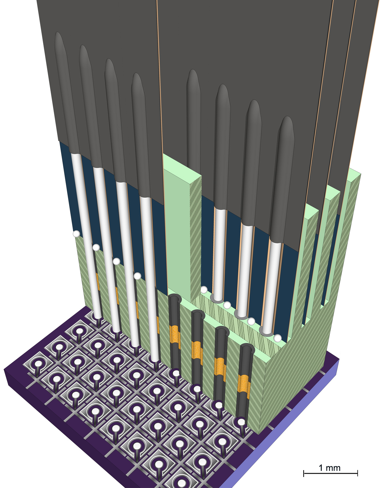
Figure 1 shows a schematic representation of the qubit wiring method proposed here, pin-chip bonding for fully vertical interconnects, which will make it possible to implement large-scale QPUs. This method is based on rectangular coaxial ribbon cables attached to micro-sized pins, forming coaxial transmission lines by means of an interposer block; the tip of each pin is bonded vertically to mating pads on the quantum chip using In. The quantum chip is patterned with a square array of thick circular pads made from In with ; the In pads can be fabricated above an underlying Al thin film, or other films. Each pad is electrically connected to an on-chip Al (or Nb) trace used to reach a qubit. The pad array is in a one-to-one correspondence with a mating pin array. Each pin is long and has a core made from SUS 304 Austenite stainless steel (or similar) with , coated first with a thick titanium nitride (TiN) film and then with a thick (or possibly thicker) In film resulting in . The TiN coating, which can be applied using physical vapor deposition, guarantees that microwave signals are carried within a superconducting region at and acts as an interdiffusion barrier Foxen et al. (2018), if necessary. The In film can be applied by means of thermal evaporation [other materials such as tin-lead (Sn-Pb) eutectic alloys may be used] and serves as the bonding agent between pin and pad.
We fabricate rectangular coaxial ribbon cables, each consisting of a thick flexible polyimide tape coated with a thick Nb film (similar to the work in Ref. Tuckerman et al. (2016)). This film is patterned to form a set of parallel transmission lines in a coplanar waveguide (CPW) design, which are then coated with a thick (or possibly thicker) Sn-Pb film. The pins are attached to the cables following this procedure:
-
(1)
The tail of each pin is placed on one signal trace of a ribbon cable.
-
(2)
another ribbon cable is flipped over and aligned with the underlying cable with a vertical offset of , exposing part of its bottom;
-
(3)
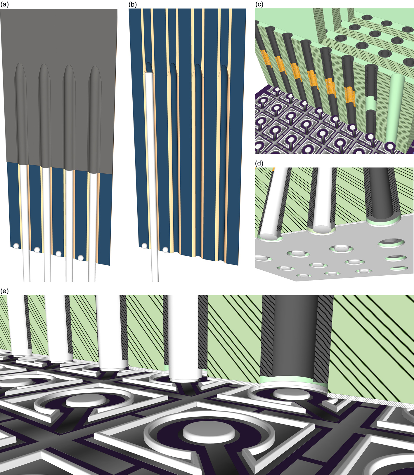
the cable-pin-cable assembly is compressed and soldered in a reflow oven at , with the front segment of each pin free hanging at the bottom of the assembly [see Fig. 2 (a) and (b)].
After the reflow step, In solder balls with are pressed on the exposed conductor of the ground traces, each of width . The In balls are placed on the ground traces by means of an XY stage equipped with micro tweezers.
Note that a slight tapering of the transmission line on the ribbon cables must be engineered in order to transition smoothly from the cable region overlapping with the circular pin to the flat cable region. This taring allows us not to increase the wiring footprint [see Fig. 2 (b)].
To form a coaxial transmission line and perform pin-pad alignment we fabricate an interposer block made of, e.g., oxygen-free high thermal conductivity (OFHC) copper (Cu), where a square array of through holes each with is made by way of fast hole drilling electrical discharge machining. Each row of holes resides at the bottom of a channel of width and depth [see Fig. 1 and Fig. 2 (c)]. The channel (groove) is fabricated by means of single-point diamond turning (SPDT) Higginbottom et al. (2018), which provides extremely high nanometric accuracy and precision and allows to trench narrow channels in Cu and possibly other materials. The aspect ratio of our channels is at a minimum , which is not terribly hard to achieve with SPDT. Boss extruders or dowels are used to align the interposer to a sample holder housing the quantum chip.
The exposed part of a cable-pin-cable assembly is inserted in one of the channels, with the front segment of each pin threaded through a matching hole in the interposer. Prior to pin insertion, the holes are filled with, e.g., STYCAST 1266 A/B 333See, e.g., http://research.physics.illinois.edu/bezryadin/labprotocol/stycast1266.pdf., which has a relative electric permittivity . Two polytetrafluoroethylene (PTFE) spacers [see Fig. 2 (c) and (d)] are used to separate the pin from the hole’s wall, realizing a coaxial transmission line. During insertion the pins are protected by means of a thick photoresist film; the photoresist on the pin’s tip is stripped prior to bonding (the resist on the exposed part of the pin simply adds to the coaxial transmission line dielectric). After a curing step at , the entire assembly is heated in a vacuum oven at , soldering the In balls to one wall of the channel. A dielectric spray or filling (grease) is used to isolate the exposed part of the transmission lines from the interposer block. The tip of each pin is adjusted to be flush with the interposer bottom surface [see Fig. 2 (d)]. All tips must be aligned vertically with a tolerance of at least pushing the pin array onto mesa stops patterned on an auxiliary Si chip. This chip is eventually substituted with the quantum chip when performing the actual pin-chip bonding step.
Note that many rows of rectangular coaxial ribbon cables will be in close proximity when wiring a large two-dimensional array of qubits. In order to shield adjacent cable rows and avoid large inter-cable crosstalk, the two outer surfaces of each polyimide tape must be coated with a thick Nb film. This conductive (superconductive below ) film not only acts as an electromagnetic shield between adjacent cable rows, but also effectively results in a stripline transmission line Collin (2001). This helps mitigate significantly the intra-cable crosstalk between adjacent transmission lines on the same tape due to a field confinement between the signal trace and outer ground larger than between the signal trace and lateral CPW grounds.
Depending on the chosen pin diameter, the characteristic impedance of the coaxial transmission line in the interposer is . We propose to depart from currently used for qubit control lines and resort to smaller impedances, where the inner conductor diameter is maximized for mechanical robustness and the outer conductor diameter is reduced to obtain smaller lines. We note that the vast majority of the control electronics used for medium-scale quantum computers is already fully custom made and, thus, can be designed with practically arbitrary values of .
The bonding procedure is realized as follows:
-
(1)
The thin In oxide layer on the pin’s outer surface is etched with hydrochloric acid Brecht et al. (2017) and the In oxide film on the pad with a plasma etch Foxen et al. (2018);
-
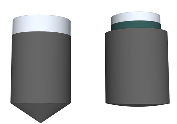
(a)
Conical bonding (see Fig. 3 left) is realized with a sharp conical pin tip that penetrates into the In layer of the pad. In this case, the pin outer surface should not be coated with In and pre-bonding oxide cleaning may be unnecessary. Using a similar pressure per pin as for flip chip, our experience with Pogo pins Béjanin et al. (2016) indicates that the pin will puncture only the first of a thick In pad;
-
(b)
Alternatively, Spherical bonding (see Fig. 3 right) is realized using a rounded spherical pin tip that is compressed onto the underlying pad with a similar pressure as for flip chip, corresponding to to per pin/pad. This pressure, which is comparable to that used in our previous work on Pogo pins Béjanin et al. (2016), will not damage the pins;
-
(a)
-
(2)
In both bonding procedures, a ultrasonic signal can be applied to ease pin-pad connection;
-
(3)
Standard In bump bonding as in flip chip is used for the ground connections at the quantum chip level. The bottom surface of the interposer block is coated with a thick In film that is bonded to an In curb on the ground planes of the quantum chip [see Fig. 2 (d) and (e)]. The PTFE spacers are flush with the uncoated Cu surface of the interposer block.
We note that, in the case of conical bonding, the pin may be coated with In or Al, the latter being stronger and more resilient during piercing. It is well known that Al diffuses very rapidly into In McRae et al. (2018), thus permitting an excellent electrical connection. Both Al and In films must be cleaned from their native oxide layers prior to piercing.
IV CONCLUSION
In the case of an interconnect with full vertical access, as for pin-chip bonding, when the second condition on dense wiring reduces to
| (4) |
without any constraint on . Considering the dimensions provided above, we find that the maximum number of qubits is limited by the qubit size; for a square chip out of a wafer, and, thus, . This is a factor of more than larger than for flip chip and, e.g., it will make it possible to implement quantum error corrected qubits Fowler et al. (2012), a remarkable number to start realize useful quantum algorithms.
Note that, in the case of flip chip, it is unpractical to adopt a very large chip. A chip, for example, would correspond to using optimal flip chip dimensions. In this case, the qubit pitch should be to fully take advantage of the chip size. Such a qubit spacing could be realized by means of qubit-resonator-qubit cells, where the resonator acts as a coherent qubit spacer. However, microwave planar resonators are bound to lengths in the few millimeter range due to their wavelength, typically larger than . For instance, in the IBM Q quantum chip Bronn et al. (2018), the qubits are spaced by ; in this case, we find . More compact coherent spacers may be realized using lumped element resonators or planar resonators with much higher resonance frequency. In all these cases, however, the spacer impact on qubit gate fidelities may be important.
Lastly, it is worth mentioning that rectangular coaxial ribbon cables can easily be engineered to embed attenuators and filters along the transmission lines, without impacting the wiring footprint. For example, Au or palladium traces can be added where required to form the large resistors used in attenuators. Infrared filters can be realized by altering the polyimide tape with a magnetically loaded black dye or a thin paint (or spray). Bundles of ribbon cables can be then pressed laterally in correspondence with attenuators or filters and heat sunk to the various stages of the DR.
Acknowledgements.
We thank our fruitful discussions with David P. DiVincenzo about qubit operation at as well as Bluhm’s group for discussions about heat shielding interposer chips.References
- Neill et al. (2018) C. Neill, P. Roushan, K. Kechedzhi, S. Boixo, S. V. Isakov, V. Smelyanskiy, A. Megrant, B. Chiaro, A. Dunsworth, K. Arya, R. Barends, B. Burkett, Y. Chen, Z. Chen, A. Fowler, B. Foxen, M. Giustina, R. Graff, E. Jeffrey, T. Huang, J. Kelly, P. Klimov, E. Lucero, J. Mutus, M. Neeley, C. Quintana, D. Sank, A. Vainsencher, J. Wenner, T. C. White, H. Neven, and J. M. Martinis, “A blueprint for demonstrating quantum supremacy with superconducting qubits,” Science 360, 195–199 (2018).
- Ladd et al. (2010) Thaddeus D. Ladd, Fedor Jelezko, Raymond Laflamme, Yasunobu Nakamura, Christopher Monroe, and Jeremy L. O’Brien, “Quantum computers,” Nature 464, 45–53 (2010).
- Clarke and Wilhelm (2008) John Clarke and Frank K. Wilhelm, “Superconducting quantum bits,” Nature 453, 1031–1042 (2008).
- Wendin (2017) G Wendin, “Quantum information processing with superconducting circuits: a review,” Reports on Progress in Physics 80, 106001 (2017).
- Knight (2017) Will Knight, “Ibm raises the bar with a 50-qubit quantum computer,” MIT Technology Review (2017).
- Giles and Knight (2018) Martin Giles and Will Knight, “Google thinks it’s close to “quantum supremacy.” here’s what that really means.” MIT Technology Review (2018).
- Montanaro (2016) Ashley Montanaro, “Quantum algorithms: An overview,” npj Quantum Information 2, 15023 (2016).
- Gottesman (2010) Daniel Gottesman, “An introduction to quantum error correction and fault-tolerant quantum computation,” Quantum Information Science and Its Contributions to Mathematics, Proceedings of Symposia in Applied Mathematics 68, 13–58 (2010).
- Nielsen and Chuang (2000) Michael A. Nielsen and Isaac L. Chuang, Quantum Computation and Quantum Information (Cambridge University Press (CUP), Cambridge, UK, 2000).
- Koch et al. (2007) Roger H. Koch, David P. DiVincenzo, and John Clarke, “Model for flux noise in squids and qubits,” Phys. Rev. Lett. 98, 267003 (2007).
- Barends et al. (2013) Rami Barends, Julian Kelly, Anthony Megrant, Daniel Sank, Evan Jeffrey, Yu Chen, Yi Yin, Ben Chiaro, Josh Mutus, Charles Neill, Peter O’Malley, Pedram Roushan, James Wenner, Theodor C. White, Aandrew N. Cleland, and John M. Martinis, “Coherent josephson qubit suitable for scalable quantum integrated circuits,” Phys. Rev. Lett. 111, 080502 (2013).
- Kelly et al. (2015) Julian Kelly, Rami Barends, Austin G. Fowler, Anthony Megrant, Evan Jeffrey, Theodore C. White, Daniel Sank, Josh Y. Mutus, Brooks Campbell, Yu Chen, Zijun Chen, Ben Chiaro, Andrew Dunsworth, Io-Chun Hoi, Charles Neill, Peter J.J. O’Malley, Christopher Quintana, Pedram Roushan, Amit Vainsencher, James Wenner, Andrew N. Cleland, and John M. Martinis, “State preservation by repetitive error detection in a superconducting quantum circuit,” Nature 519, 66–69 (2015).
- Versluis et al. (2017) R. Versluis, S. Poletto, N. Khammassi, B. Tarasinski, N. Haider, D. J. Michalak, A. Bruno, K. Bertels, and L. DiCarlo, “Scalable quantum circuit and control for a superconducting surface code,” Phys. Rev. Applied 8, 034021 (2017).
- Otterbach et al. (2017) J. S. Otterbach, R. Manenti, N. Alidoust, A. Bestwick, M. Block, B. Bloom, S. Caldwell, N. Didier, E. Schuyler Fried, S. Hong, P. Karalekas, C. B. Osborn, A. Papageorge, E. C. Peterson, G. Prawiroatmodjo, N. Rubin, Colm A. Ryan, D. Scarabelli, M. Scheer, E. A. Sete, P. Sivarajah, Robert S. Smith, A. Staley, N. Tezak, W. J. Zeng, A. Hudson, Blake R. Johnson, M. Reagor, M. P. da Silva, and C. Rigetti, “Unsupervised machine learning on a hybrid quantum computer,” (2017), arXiv:1712.05771 .
- Martinis (2015) John M. Martinis, “Qubit metrology for building a fault-tolerant quantum computer,” npj Quantum Information 1, 15005 (2015).
- Tuckerman et al. (2016) David B Tuckerman, Michael C Hamilton, David J Reilly, Rujun Bai, George A Hernandez, John M Hornibrook, John A Sellers, and Charles D Ellis, “Flexible superconducting nb transmission lines on thin film polyimide for quantum computing applications,” Superconductor Science and Technology 29, 084007 (2016).
- Béjanin et al. (2016) J. H. Béjanin, T. G. McConkey, J. R. Rinehart, C. T. Earnest, C. R. H. McRae, D. Shiri, J. D. Bateman, Y. Rohanizadegan, B. Penava, P. Breul, S. Royak, M. Zapatka, A. G. Fowler, and M. Mariantoni, “Three-dimensional wiring for extensible quantum computing: The quantum socket,” Phys. Rev. Applied 6, 044010 (2016).
- Wenner et al. (2011) James Wenner, Matthew Neeley, Radoslaw C. Bialczak, Michael Lenander, Erik Lucero, Aaron D. O’Connell, Daniel Sank, Haohua Wang, Martin Weides, Andrew N. Cleland, and John M. Martinis, “Wirebond crosstalk and cavity modes in large chip mounts for superconducting qubits,” Superconductor Science and Technology 24, 065001 (2011).
- Earnest et al. (2018) Carolyn T Earnest, Jérémy H Béjanin, Thomas G McConkey, Evan A. Peters, Andreas Korinek, Hui Yuan, and Matteo Mariantoni, “Substrate surface engineering for high-quality silicon/aluminum superconducting resonators,” Superconductor Science and Technology (2018).
- Bronn et al. (2018) Nicholas T Bronn, Vivekananda P Adiga, Salvatore B Olivadese, Xian Wu, Jerry M Chow, and David P Pappas, “High coherence plane breaking packaging for superconducting qubits,” Quantum Science and Technology 3, 024007 (2018).
- Rosenberg et al. (2017) Danna Rosenberg, David Kim, Rabindra Das, Donna-Ruth Yost, Simon Gustavsson, David Hover, Philip Krantz, A. Melville, Livia Racz, Gabriel O. Samach, Steven J. Weber, Fei Yan, Jonilyn Yoder, Andrew J. Kerman, and William D. Oliver, “Building logical qubits in a superconducting quantum computing system,” npj Quantum Information 3 (2017), doi:10.1038/s41534-017-0044-0.
- Foxen et al. (2018) B Foxen, J Y Mutus, E Lucero, R Graff, A Megrant, Yu Chen, C Quintana, B Burkett, J Kelly, E Jeffrey, Yan Yang, Anthony Yu, K Arya, R Barends, Zijun Chen, B Chiaro, A Dunsworth, A Fowler, C Gidney, M Giustina, T Huang, P Klimov, M Neeley, C Neill, P Roushan, D Sank, A Vainsencher, J Wenner, T C White, and John M Martinis, “Qubit compatible superconducting interconnects,” Quantum Science and Technology 3, 014005 (2018).
- Das et al. (2018) R. Das, J. Yoder, D. Rosenberg, D. Kim, D. Yost, J. Mallek, D. Hover, V. Bolkhovsky, A. Kerman, and W. Oliver, “Cryogenic qubit integration for quantum computing,” in 2018 IEEE 68th Electronic Components and Technology Conference (ECTC) (2018) pp. 504–514.
- McDermott et al. (2018) R McDermott, M G Vavilov, B L T Plourde, F K Wilhelm, P J Liebermann, O A Mukhanov, and T A Ohki, “Quantum–classical interface based on single flux quantum digital logic,” Quantum Science and Technology 3, 024004 (2018).
- Patra et al. (2018) B. Patra, R. M. Incandela, J. P. G. van Dijk, H. A. R. Homulle, L. Song, M. Shahmohammadi, R. B. Staszewski, A. Vladimirescu, M. Babaie, F. Sebastiano, and E. Charbon, “Cryo-cmos circuits and systems for quantum computing applications,” IEEE Journal of Solid-State Circuits 53, 309–321 (2018).
- Valenzuela et al. (2006) Sergio O. Valenzuela, William D. Oliver, David M. Berns, Karl K. Berggren, Leonid S. Levitov, and Terry P. Orlando, “Microwave-induced cooling of a superconducting qubit,” Science 314, 1589–1592 (2006), http://science.sciencemag.org/content/314/5805/1589.full.pdf .
- Park et al. (2016) Daniel K. Park, Nayeli A. Rodriguez-Briones, Guanru Feng, Robabeh Rahimi, Jonathan Baugh, and Raymond Laflamme, “Heat bath algorithmic cooling with spins: Review and prospects,” in Electron Spin Resonance (ESR) Based Quantum Computing, edited by Takeji Takui, Lawrence Berliner, and Graeme Hanson (Springer New York, New York, NY, 2016) pp. 227–255.
- Note (1) Note that, pin-chip bonding is not limited to this specific qubit footprint. Smaller qubit footprints and different qubit designs can me considered as well.
- Note (2) See, e.g., http://www.scanditron.com/sites/default/files/material/heraeus_bondingwire_brochure.pdf or https://www.cirexx.com/wire-bonding/.
- Higginbottom et al. (2018) Daniel B. Higginbottom, Geoff T. Campbell, Gabriel Araneda, Fengzhou Fang, Yves Colombe, Ben C. Buchler, and Ping Koy Lam, “Fabrication of ultrahigh-precision hemispherical mirrors for quantum-optics applications,” Scientific Reports 8 (2018), 10.1038/s41598-017-18637-8.
- Note (3) See, e.g., http://research.physics.illinois.edu/bezryadin/labprotocol/stycast1266.pdf.
- Collin (2001) Robert E. Collin, Foundations for Microwave Engineering - 2nd Edition (Institute of Electrical & Electronics Engineers (IEEE), Inc., and John Wiley & Sons, Inc., New York, NY, and Hoboken, NJ, USA, 2001).
- Brecht et al. (2017) Teresa Brecht, Yiwen Chu, Christopher Axline, Wolfgang Pfaff, Jacob Z. Blumoff, Kevin Chou, Lev Krayzman, Luigi Frunzio, and Robert J. Schoelkopf, “Micromachined integrated quantum circuit containing a superconducting qubit,” Phys. Rev. Applied 7, 044018 (2017).
- McRae et al. (2018) C. R. H. McRae, J. H. Béjanin, C. T. Earnest, T. G. McConkey, J. R. Rinehart, C. Deimert, J. P. Thomas, Z. R. Wasilewski, and M. Mariantoni, “Thin film metrology and microwave loss characterization of indium and aluminum/indium superconducting planar resonators,” Journal of Applied Physics 123, 205304 (2018).
- Fowler et al. (2012) Austin G. Fowler, Matteo Mariantoni, John M. Martinis, and Andrew N. Cleland, “Surface codes: Towards practical large-scale quantum computation,” Phys. Rev. A 86, 032324 (2012).