Ab initio simulation of the structure and transport properties of zirconium and ferromagnetic cobalt contacts on the two-dimensional semiconductor WS2
Abstract
Using density-functional theory calculations, the atomic and electronic structure of single-layer WS2 attached to Zr and Co contacts are determined. Both metals form stable interfaces that are promising as contacts for injection of n-type carriers into the conduction band of WS2 with Schottky barriers of 0.45eV and 0.62eV for Zr and Co, respectively. With the help of quantum transport calculations, we address the conductive properties of a free-standing WS2 sheet suspended between two Zr contacts. It is found that such a device behaves like a diode with steep I-V characteristics. Spin-polarized transport is calculated for such a device with a floating-gate Co electrode added. Depending on the geometrical shape of the Co gate and the energy of the carriers in WS2, the transmission of spin majority and minority electrons may differ by up to an order of magnitude. Thus the steep I-V characteristics of the nanoscale device makes it possible to realize a spin filter.
I Introduction
Transition metal dichalcogenide (TMDC) monolayers (MLs) have emerged as a promising 2D crystal family with several characteristic features. Their direct band gap and the strong spin-orbit coupling combined with the lack of inversion symmetry leads to a unique coupling of the spin and valley degrees of freedom. Due to this distinct feature, elastic scattering of charge carriers is possible only by simultaneously flipping the spins of two carriers, and this severe restriction leads to small inter-valley scattering rates and therefore long spin and valley lifetimes. These properties make the TMDCs promising candidates for future nanoscale electronics. The role of contacts of 2D materials is an important issue for electronics device performance. Due to the semiconducting nature of 2D TMDCs, metal contacts are likely to create Schottky barriers. On the one hand, these barriers can be useful in coping with the impedance mismatch problem Schmidt et al. (2000), as has been pointed out in the field of spintronicsFert and Jaffrès (2001). On the other hand, an elimination of Schottky barriers is desirable if the injection current should be maximized.
Several studies have focused on achieving desirable contact properties. Experimentally, the growth of metals on TMDCs have affected the resulting morphologies; for example, Pd grows on MoS2 as a uniform layer while Au and Ag grow in clustersGong et al. (2013). Both experimentsLiu et al. (2013) and simulations Kang et al. (2012) have predicted that Ti as contact metal to MoS2 helps to eliminate the Schottky barrier. In 2016, Farmanbar and Brocks calculated the contact between MoS2 and various metal surfaces, such as Au, Ag, Cu, and Ni. Their results show that MoS2 interacts strongly with transition metals Farmanbar and Brocks (2016). DFT calculations have shown that the tunnel barrier between Pd and monolayer MoS2 can be reduced to negligible heightKang et al. (2012). Kang et al. studied the interface between monolayer MoS2 and WSe2 and various metals (including In, Ti, Au, Pd, Mo, and W) by DFT calculations. Their results show that Ti and Mo are the best metals for n-type contacts on monolayer MoS2, while Pd was found to be the best metal for monolayer WSe2, both metals forming n-type contacts Kang et al. (2014).
Most studies examining TMDCs for device applications have reported on interfaces between TMDC MLs and various non-magnetic metals. Only few studies have been focused on interfaces between ferromagnetic metals and TMDC MLs. Experimentally, magnetic tunnel junctions of Fe/MoS2/Fe have been investigated and the results demonstrated that MoS2 became conductive when the MoS2 spacer contained only one or two layers Dolui et al. (2014). Chen et al. have investigated properties of single-layer MoS2 with Co electrodes and measured the Schottky barrier height in this system. They found that by inserting a thin MgO oxide barrier between the Co electrode and the MoS2 flake, the Schottky barrier height can be reduced Chen et al. (2013). Finally, Garandel et al. have recently studied the electronic structure of Co/MoS2 interfaces and the Schottky barrier height of this system has been estimated to be eV Garandel et al. (2017).
It is important to understand the nature of the electronic interface between metals and a TMDCs monolayer. Hence, in this paper, we employ first principles computations to study the properties of the interface WS2/metal. Slabs of the hexagonally close-packed (hcp) metals Zr and Co are used to model the (0001) surfaces of Zr bulk or Co bulk, which serve as templates to place the hexagonal layer of WS2. WS2 has attracted appreciable interest among TMDC monolayers due to the presence of a high valence band splitting and a high mobility. We considered Zr and Co as suitable candidates for contact properties. Zr emerges as an ideal candidate with only 1.5% mismatch to WS2. Co appears less suitable at first sight due to a large lattice mismatch, but spin-injection from such a high-Curie-temperature ferromagnetic metal to a single TMDC layer is very important since it would give access to TMDC-based spintronic devices.
II Computational details
All presented calculations are performed in the frame- work of the spin-polarized Kohn-Sham density functional theory by using the all-electron full-potential code FHI-aimsBlum et al. (2009). The generalized gradient approximation (GGA) in the Perdew-Burke-Ernzerhof (PBE)Perdew et al. (1996) implementation is applied as the exchange-correlation functional. All calculations reported here are done in the scalar-relativistic approximation with the so-called ’tight’ settings for the basis set and on grids in the FHI-aims code. A convergence criterion of eV for the total energy and e/Å3 for the charge density were employed. To treat van der Waals (vdW) interactions, we apply the Tkatchenko-Scheffler (TS) methodTkatchenko and Scheffler (2009), i.e. a density-dependent pairwise interaction is added to the exchange-correlation energy to describe the interfaces Co/WS2 and Zr/WS2. For the Zr or Co metal electrodes, only the interface Zr or Co layer takes part in the vdW interaction, and modified vdW parameters according to the TS scheme for surfaces Ruiz et al. (2012) are used. Van der Waals interactions between Co or Zr atoms having a bulk environment are disregarded.
Before constructing supercells for calculations of WS2 on cobalt, first the theoretical lattice constants in the hexagonal plane of hcp bulk cobalt and of a WS2 ML were obtained to be Å and Å, respectively, in satisfactory agreement with the experimental values of 2.49Å and 3.08Å Fox and Jansen (1999); Zhang et al. (2017); Kang et al. (2013), respectively.
For the Co metal electrode, we consider two possible orientations of the WS2 layer. In the first orientation, termed Co/WS, the lattice vectors of the Co(0001) and the WS2 unit cells are collinear. The Co/WS hybrid structure was modeled as a periodic slab by setting the supercell lattice parameter to Å, corresponding to primitive cobalt cells and primitive WS2 cells.
As an alternative, we consider a supercell in which the misfit strain between Co and WS2 is (almost) compensated only in one crystallographic direction, while there is a relatively large strain in the perpendicular direction. This situation, termed Co/WS, is realized if the WS2 monolayer is deposited with a rotation of 90∘ with respect to the cobalt slab. We used a supercell of WS2 matched to a supercell of the Co(0001) surface. In this situation, a pre-strain in WS2 is introduced that is 1.73% for Co/WS and 10.28% at the Co/WS interface. .pdf
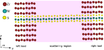
The calculated in-plane lattice constant of bulk hcp Zr is Å, in perfect match with the experimental value of 3.23Å Willaime (2003). To model the Zr/WS2 interface, the WS unit cell is adjusted to the unit cell of Zr(0001). In all calculations, the WS2 layer was attached only to one side of the metal slab, and a 15Å vacuum layer was added to prevent artificial interaction due to the periodic boundary conditions perpendicular to the surface. In the geometry optimizations, a convergence criterion of eV/Å for the residual forces was adopted. The Brillouin zone integrations were performed by using meshes of , and k-points for Co/WS , Co/WS and Zr/WS2, respectively. Once the atomic structure has been obtained, we include spin-orbit coupling effects on the electronic structure via the second-order variational method implemented in FHI-aims Huhn and Blum (2017).
For the simulation of the transport characteristics of spintronics devices based on a WS2 sheet, we used the PWCOND codeJoon Choi and Ihm (1999); Smogunov et al. (2004) of the Quantum Espresso packageGiannozzi et al. (2009), that implements the Landauer-Büttiker approachBüttiker (1986) to quantum transport. This code allows us to restrict the electronic structure calculation to the valence electrons only, using ultrasoft pseudo-potentials (US-PPs)Vanderbilt (1990) to model the electron-ion interactions. Transport in heterostructuresGeisler and Kratzer (2015) can be treated by taking a momentum component perpendicular to the transport direction into account and averaging the transmission probabilities,
| (1) |
where is the transmission probability of an electron with energy and perpendicular momentum , and is a weighting factor following from symmetry considerations. As before, the PBE generalized gradient approximationPerdew et al. (1996) of the exchange-correlation functional was employed. The electronic wave functions were expanded in a plane-wave basis set with an energy cutoff of 40 Ry. The vdW interactions were treated by the Grimme-D2 methodGrimme (2006). In contrast to the adsorption study, we consider a free-standing, single-layer WS2 sheet as building block of an envisaged spintronics device. The electrical current flows along the zig-zag chains of WS2, taken to define the direction, while the WS2 sheet is assumed to be infinitely extended in the perpendicular -direction. To establish electrical contact, the sheet is clamped between Zr electrodes touching the sheet both from above and below, see Fig. 1. The supercell of the electrode region is constructed from a rectangular cell of WS2 with side length and containing four W and 8 S atoms attached to Zr(0001) surfaces. For the free-standing part of the WS2 sheet as well as for the clamped part the lattice constant of WS2 (Å) was used; i.e. the lattice parameter of Zr in the electrode was adjusted to . Periodic boundary conditions are assumed in the and directions for the calculations of the electronic ground state. The Brillouin zone of the leads and of the center region have been sampled using a 12112 and 1211 Monkhorst-Pack grid, respectively. For geometry optimizations, the Hellmann-Feynman forces were required to be smaller than Ry/bohr.
III RESULTS AND DISCUSSION
III.1 Geometry and stability of WS2-metal interface
In order to determine the stable location of WS2 on Co and Zr slabs, the binding energy () was calculated as
| (2) |
where and are the total energies of the M slab (cobalt, zirconium) and of the WS2 sheet strained to the lattice constant appropriate for each case. We first determine the equilibrium geometry of Zr/WS2 and then investigate the stable configuration of WS2 (in both rotational variants) on Co(0001).
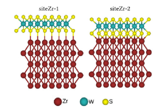
WS2-Zr interface: A five-layer Zr slab unit cell was used in the calculations, where the two bottom layers were fixed to the PBE bulk-optimized positions whereas the three top Zr layers were relaxed. We constructed two structures of Zr/WS2: (i) siteZr-1 configuration, in which the W atom of the WS2 layer sits above the Zr atom of the second and forth Zr layer, and the S layers are in line with the Zr atoms of the first, third and fifth Zr layer. (ii) siteZr-2 configuration, in which the W atom of the WS2 layer is aligned with the Zr atoms of the first, third and fifth layer, and the S atoms are located above the Zr atoms of the second and fourth Zr layer. Optimized geometric structures are shown in Fig. 2. We found that siteZr-2 is the most favorable configuration. The equilibrium distances for siteZr-1 and siteZr-2 are 2.64 and 2.57Å, respectively. These interatomic distances are similar to the bond lengths which have been measured in the bulk zirconium sulfide (ZrS2) crystal with rocksalt structure (2.58Å, Ref. Nguyen, 1980). The binding energies Eb follow the ordering [siteZr-2] [siteZr-1] eV; i.e., smaller correlates with a larger binding energy.
Co/WS2 interface: In the geometry optimization Co/WS and Co/WS , the WS2 monolayer and the top cobalt layer were allowed to relax while the remaining bottom layers were constrained to their bulk positions.
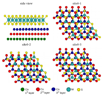
In order to study the structural and magnetic properties of Co/WS, we first looked for the stable configuration of these heterostructures. In this regard, we gradually move the WS2 parallel to the Co(0001) surface. Seven atomic configurations of the interface atoms were considered. After optimizing the structures from these seven initial configurations, we found that four configurations transformed to the site0-3 structure. The structures found to be stable are sketched in Fig. 3. The calculated binding energy as well as other structural parameters of the investigated configuration of Co/WS are listed in Table 1.
| Co/WS | |||||
|---|---|---|---|---|---|
| M | |||||
| site0-1 | 39.2 | -19.72 | 1.654 | 2.34 | |
| site0-2 | 1.5 | -19.76 | 1.652 | 2.32 | |
| site0-3 | 0.0 | -19.77 | 1.652 | 2.31 |
Our calculations show that site0-3 is the most stable configuration of Co/WS. When the WS2 monolayer is in contact to cobalt, the equilibrium distances range from 2.31 – 2.34Å. We can see that the smaller generally correlates with a larger binding energy and the site0-3 system has strong interface bonding. These distances are close to experimental data obtained for bulk CoS2 with the pyrite structure (2.32Å, Ref. Nowack et al., 1991).
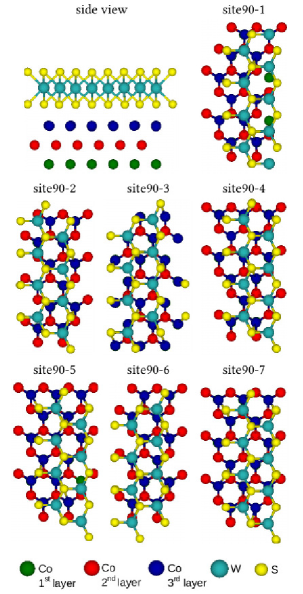
To investigate the stable structure of Co/WS, we moved WS2 on the Co(0001) surface. All optimized geometric structures are shown in Fig. 4. We found that site1-90 is the most favorable configuration (see Table 2). The differences in binding energy between site1-90 and the other configurations are of the order of a few meV.
| Co/WS | |||||
|---|---|---|---|---|---|
| M | |||||
| site90-1 | 0.0 | -5.146 | 1.636 | 2.342 | |
| site90-2 | 0.021 | -5.145 | 1.636 | 2.343 | |
| site90-3 | 4.792 | -5.141 | 1.635 | 2.341 | |
| site90-4 | 0.002 | -5.145 | 1.636 | 2.343 | |
| site90-5 | 4.863 | -5.140 | 1.635 | 2.341 | |
| site90-6 | 4.884 | -5.140 | 1.635 | 2.341 | |
| site90-7 | 0.181 | -5.144 | 1.636 | 2.343 |
We investigate the magnetic properties of the most stable of both Co/WS and Co/WS. The results indicate that the average local magnetic moment of a Co atom for Co/WS (1.654/Co) and Co/WS (1.636/Co) are lower than in bulk Co (1.69/Co) with the hcp structure. To understand the magnetic moment of each atom in both structures, we considered the Mulliken population analysis for these systems. In the interface Co layer, the magnetic moments are generally reduced compared to bulk Co and their values scatter between 1.45 and 1.67 . The middle layer almost recovers the magnetic moments of bulk Co, while the Co atoms in the bottom layer of the slab with its free surface reach 1.75/Co for both Co/WS2 slabs. The covalent bonding between interface Co and S atoms reduces the spin magnetic moment of the Co layer, while the interface S atoms become slightly magnetic (0.025/S).
Finally, to facilitate a direct comparison among Zr/WS2, Co/WS and Co/WS, the binding energy per interface atom was calculated for all three structures. In all three interfaces, the S atoms are covalently bonded to Zr and Co, which means that the WS2 single layer is covalently bound to the Co and Zr slabs and the van der Waals interaction plays only a minor role. The results show that the zirconium interface has a much stronger binding energy, eV/Zr atom, with WS2 than cobalt. In Co/WS2, we find that the binding energy between WS2 oriented in the same way as the Co(0001) surface (0.79 eV/Co atom) is higher than for the Co/WS structure (0.43 eV/Co atom). This is because the alignment of the two hexagonal lattices of WS2 and Co(0001) allows for better strain accommodation in the Co/WS interface.
III.2 Electronic structure of WS2-metal interfaces
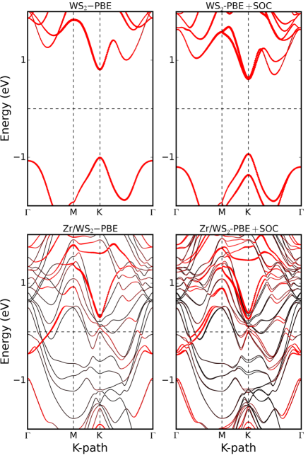
The orbital-projected electronic band structure of free-standing WS2 and of the interfacial systems with Zr and Co are investigated without (PBE) and with (PBE+SOC) spin-orbit coupling; and the results are presented in Fig.s 5 and 6. Orbital-projected electronic bands are displayed only for W atoms because the S, Zr and Co atoms are rather light and we therefore expect their orbitals not to be changed significantly under SOC. The free-standing monolayer WS2 is a direct-gap semiconductor with a Kohn-Sham gap of 1.82 eV (1.54 eV when including SOC) located at the point of the Brillouin zone, in agreement with previous calculations Zibouche et al. (2014); Zhang et al. (2017); Kang et al. (2013). As indicated by the red color in Fig. 5, both the valence band maximum (VBM) and the conduction band minimum (CBM) of WS2 are mainly composed of W 5d orbitals. Taking into account spin-orbit coupling, we observe a large splitting of the VBM (420 meV) at the K point in the first Brillouin zone (see Fig. 5). The splitting for the CBM is 30 meV and thus much smaller than the VBM splitting, in agreement with previous studies Zibouche et al. (2014); Absor et al. (2016). As can be observed in Fig. 5, the band structure of WS2 is strongly modified by the interface with Zr. The semiconducting gap of WS2 has disappeared and the Zr atoms introduce occupied bands into the gap which results in the Zr/WS2 system displaying metallic behavior. In particular, an interface state along – M with strong W 5d orbital character is formed that disperses upward and crosses the Fermi level. The CBM of WS2 is still visible in the projection onto the W 5d orbitals as a parabolic band around the K point located eV above the Fermi level. By comparing the band structure obtained with and without SOC, one notices that the position of the Fermi level and the bands derived from Zr orbitals are almost unaffected. In the W-derived interface state and in the CBM at the point, a lifting of band degeneracy due to SOC is observed.
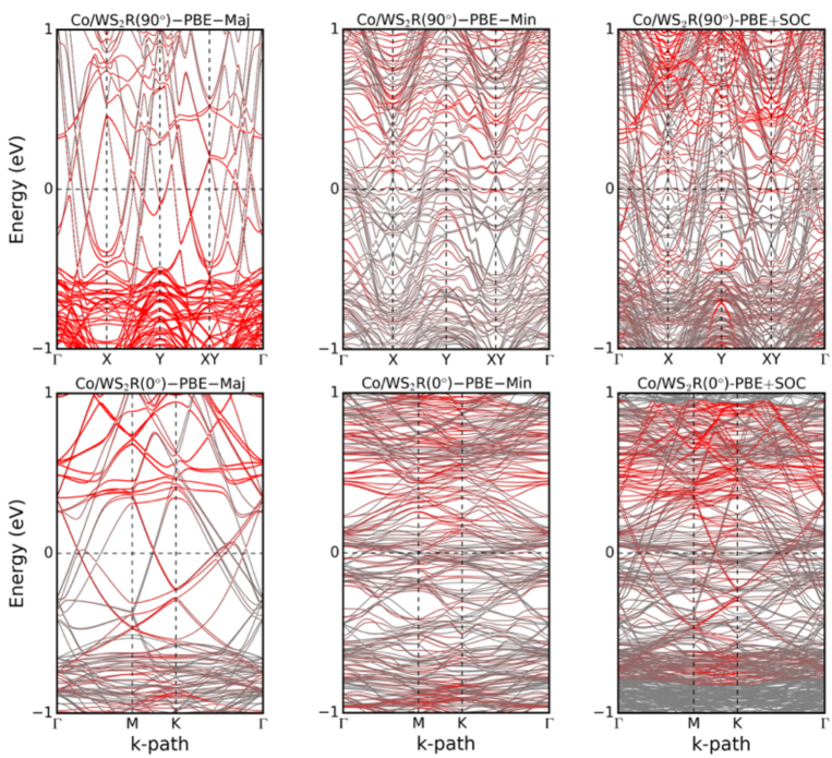
To analyze the band structure for the Co contact, we performed a similar analysis for the Co/WS and Co/WS interfaces. We observe that also the Co interface causes the semiconducting character of free-standing WS2 to disappear. New states cross the Fermi level, both for the majority and the minority spin electrons (see Fig. 6), and consequently the system behaves like a metal. In the majority spin band structures of both the Co/WS and Co/WS interfaces one can observe the fully occupied Co 3d states below eV. Some hybridization of these valence band states with the W 5d states is noticeable, but occurs far below the Fermi level. The contributions of the bands originating from WS2 are most pronounced in the conduction band of the Co/WS and Co/WS interfaces and start at eV above in the majority spin channel. In the minority spin band structures of both the Co/WS and Co/WS a huge number of bands is observed near . However, most of these bands are only weakly dispersive and originate from partially occupied Co 3d rather than from W-derived orbitals. Electronic states with a mixed character start at eV above . When SOC is included, the distinction between majority and minority spin states is no longer possible, but the combined band structure of both spins is very similar to a superposition of both spin band structures obtained previously without SOC. In the bands crossing , a clear effect of SOC, e.g. SOC-induced avoided band crossings, is not observable. Also, the magnetic moments of the Co atoms change very little, by less than 1%.
III.3 Schottky barrier at WS2-metal interfaces
 |
|
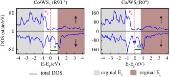 |
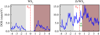
To evaluate the Schottky barrier height (SBH) between the metal and the intrinsic (undoped) semiconductor WS2, the total DOS of the M/WS2 (M=Zr,Co) interface displayed in Fig. 7 is compared to the DOS of single-layer, free-standing WS2. The Schottky barrier can be estimated from the energy difference between of the interface system and the conduction band minimum (CBM) of WS2 located at the point in the Brillouin zone. The 1s core level of W is used as a common reference point for the Fermi levels both in the interface and in pure WS2. As is seen from the figure, after interfacing WS2 with Zr, the Fermi level is located above mid-gap, closer to the CBM, indicating the possibility to inject n-type carriers (electrons) into WS2. Including the effect of spin-orbit coupling, the Zr contact to the WS2 monolayer shows a SBH of meV. Furthermore, the Co/WS contact is found to be an n-type contact, too, as seen in Fig. 7. This is in line with recently reported experiments and calculations for the Co contact with a MoS2 monolayer Garandel et al. (2017); Chen et al. (2013). The Schottky barriers are and 830 meV for Co/WS and Co/WS, respectively. When SOC is neglected, the electronic structure of the interfaces changes very little, but the gap of WS2 and the position of in intrinsic WS2 are affected (cf. Fig. 5). As a result, the SBHs for all metal contacts are increased by 140 meV if SOC is neglected.
III.4 Quantum transport at WS2 and Co/WS2
Since the CBM and VBM of WS2 are both located a the point, the WS2 sheet in a nanoscale transistor should preferentially be oriented in such a way that the current flows along the direction in the Brillouin zone, i.e. along the atomic zig-zag chains of WS2 in real space. The knowledge gained from the adsorption studies reported above are used to construct atomistic models of nanoscale spintronics devices. The most stable configurations of Zr/WS2 and Co/WS2 follow from the results of the previous section. Although Co/WS is more stable than Co/WS, we used the latter interface geometry to model a stripe of Co deposited on WS2 because this leads to a computationally tractable set-up. A Co stripe with Co/WS would require a much larger supercell with more than 600 atoms, and such a system is too large for a quantum transport calculation even on a supercomputer. For comparison, we also consider a smaller system, a Co cluster deposited on WS2.
The electronic conductance is calculated with the PWCOND code using an open system consisting of (i) a scattering region comprising the WS2 monolayer and a chosen interface to the Zr/WS2 electrodes, and (ii) the left and right (in principle semi-infinite) Zr/WS2 leads. The scattering region has to be large enough to avoid the interaction between right and left leads. In our calculations, the length of this region is 36.70 Å along the transport direction (twelve unit cells between the electrodes) that included 24 Å free-standing WS2 and 12.70 Å Zr/WS2, see Fig. 1. The leads are described by calculating the complex band structure of a periodic supercell containing four bottom layers and three top layers of Zr on WS2.
| a) |
 |
| b) |
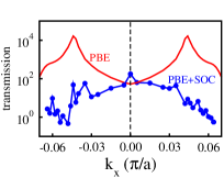 |
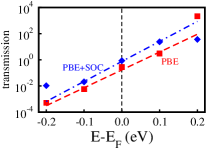
First we consider the quantum-mechanical transmission of a clean WS2 sheet clamped between two Zr contacts. For injection into the conduction band of WS2, the electrons must overcome a barrier (for macroscopic devices equal to the Schottky barrier calculated above). This is in line with the transmission exponentially increasing with electron energy, as shown in Fig. 8a) both for the calculations with and without SOC. This device works like a diode with an I-V-characteristics described by for small electron energies. Following eq. 1, electrons with all possible momenta perpendicular to the transport direction contribute to the overall transmission. With our choice of the supercell, the point is folded back to the point of the supercell; thus we expect the main contribution from electrons with . This is confirmed by the results of the PBE+SOC calculations, see Fig. 8a). However, in the calculations neglecting SOC, a sharp rise of is observed for electrons with an energy of 0.2eV above . Analyzing the transmission as function of , we find that this rise is due to maxima at , see Fig. 8b). We ascribe this observation to quantum-mechanical transmission resonances that depend both on the de Broglie wave length of the transmitted electron in the conductive channel as well as on the finite channel length. We note that, in the calculations neglecting SOC, states with wave vector and must be equivalent due to time-reversal symmetry. In the calculations including SOC, transport with wave vector and are no longer equivalent, but correspond to electrons at the inequivalent points and in the Brillouin zone of WS2. This also shows up in the asymmetry of the lower curve in Fig. 8b).
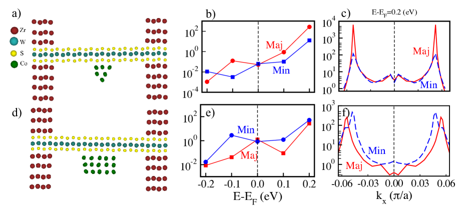
Next we are adding a Co cluster or a Co stripe in the center region, as shown in Fig. 9a) and d), and relax the geometry until we find a stable interface. The magnetization of Co breaks the time-reversal symmetry in the channel and mixes the and valleys of WS2. Because of this mixing and the qualitative similarity of the results for with and without SOC, we consider it sufficient to study the transmission in the presence of a Co gate electrode without SOC. In Fig. 9b) and e), we can see plots of the spin-dependent transmission for the WS2/Co cluster and the WS2/Co stripe. As an overall trend, the transmission curves are still increasing with energy, as in the case of pure WS2, but show additional structure. The absolute value of the transmission is lower than in the clean case. Both observations point to a small additional barrier for the electrons imposed by the proximity of the Co cluster or stripe. This proximity effect is spin-dependent. For the WS2/Co stripe the majority spin transmission is mostly (in particular for ) smaller than the minority spin transmission, while this trend is reversed for WS2/Co cluster. We attribute these observations to quantum-mechanical interference effects which play a role in nanoscale devices such as the one considered here. The relation between a change in the channel potential and a change in transmission is, however, a subtle one, since not only the barrier height, but also the exact geometry and abruptness of the barrier affect the quantum-mechanical transmission amplitude. Analyzing the transmission as function of for the highest electron energy investigated, eV, we observe that the transmission resonance found for the pure WS2 sheet has become very sharp by the addition of the Co gate, and displays different maximum transmission in the majority and the minority spin channel, see Fig. 9c). The effect of a stripe-shaped Co gate is somewhat different: The resonances have nearly equal height in both spin channels, but their maxima as function of are slightly shifted, see Fig. 9f). These equal heights explain why, nder ’open gate’ condition at eV, both spin channels show nearly equal overall transmission and the spin polarization of the transmitted current tends to vanish.
IV Conclusion
In conclusion, we employed first-principles calculations to investigate various components of a future spintronics device based on a single-layer WS2 sheet. Our calculations show that both Zr and Co can be used to form stable contacts on WS2 that allow for injection of carriers into the conduction band. The most stable atomic structure of the interface can be deduced from the calculations, and it is shown that the magnetic moment of the Co surface persists in the presence of WS2. Moreover, quantum-mechanical transport calculations show that a single-layer WS2 sheet clamped between Zr electrodes behaves like a Schottky diode with a sharp I-V-characteristics. A gate electrode of Co can be used to control the spin polarization of the current. For the nanoscale device studied by us, we find that the spin polarization sensitively depends on the geometrical shape of the gate and on the energy of the electrons. As a direction for future work, one could attempt a generalization of these findings to larger devices where semiclassical transport theory would be applicable.
Acknowledgements
H.K. is grateful to the Iranian Ministry of Science, Research and Technology for a travel scholarship. We gratefully acknowledge the computing time granted by the Center for Computational Sciences and Simulation (CCSS) of the University of Duisburg-Essen and provided on the supercomputer magnitUDE (DFG Grant No. INST 20876/209-1 FUGG and INST 20876/243-1 FUGG) at the Zentrum für Informations-und Mediendienste (ZIM).
References
- Schmidt et al. (2000) G. Schmidt, D. Ferrand, L. W. Molenkamp, A. T. Filip, and B. J. van Wees, Phys. Rev. B 62, 4790 (2000).
- Fert and Jaffrès (2001) A. Fert and H. Jaffrès, Phys. Rev. B 64, 184420 (2001), URL https://link.aps.org/doi/10.1103/PhysRevB.64.184420.
- Gong et al. (2013) C. Gong, C. Huang, J. Miller, L. Cheng, Y. Hao, D. Cobden, J. Kim, R. S. Ruoff, R. M. Wallace, K. Cho, et al., ACS Nano 7, 11350 (2013), pMID: 24219632, URL https://doi.org/10.1021/nn4052138.
- Liu et al. (2013) W. Liu, J. Kang, W. Cao, D. Sarkar, Y. Khatami, D. Jena, and K. Banerjee, in 2013 IEEE International Electron Devices Meeting (2013), pp. 19.4.1–19.4.4, ISSN 2156-017X.
- Kang et al. (2012) J. Kang, D. Sarkar, W. Liu, D. Jena, and K. Banerjee, in 2012 IEEE International Electron Devices Meeting (2012), pp. 17.4.1–17.4.4 URL https://doi.org/10.1109/IEDM.2012.6479060.
- Farmanbar and Brocks (2016) M. Farmanbar and G. Brocks, Phys. Rev. B 93, 085304 (2016), URL https://link.aps.org/doi/10.1103/PhysRevB.93.085304.
- Kang et al. (2014) J. Kang, W. Liu, D. Sarkar, D. Jena, and K. Banerjee, Phys. Rev. X 4, 031005 (2014), URL https://link.aps.org/doi/10.1103/PhysRevX.4.031005.
- Dolui et al. (2014) K. Dolui, A. Narayan, I. Rungger, and S. Sanvito, Phys. Rev. B 90, 041401 (2014), URL https://link.aps.org/doi/10.1103/PhysRevB.90.041401.
- Chen et al. (2013) J.-R. Chen, P. M. Odenthal, A. G. Swartz, G. C. Floyd, H. Wen, K. Y. Luo, and R. K. Kawakami, Nano Letters 13, 3106 (2013), pMID: 23746085, URL https://doi.org/10.1021/nl4010157.
- Garandel et al. (2017) T. Garandel, R. Arras, X. Marie, P. Renucci, and L. Calmels, Phys. Rev. B 95, 075402 (2017), URL https://link.aps.org/doi/10.1103/PhysRevB.95.075402.
- Blum et al. (2009) V. Blum, R. Gehrke, F. Hanke, P. Havu, V. Havu, X. Ren, K. Reuter, and M. Scheffler, Comp. Phys. Commun. 180, 2175 (2009).
- Perdew et al. (1996) J. P. Perdew, K. Burke, and M. Ernzerhof, Phys. Rev. Lett. 77, 3865 (1996), URL https://link.aps.org/doi/10.1103/PhysRevLett.77.3865.
- Tkatchenko and Scheffler (2009) A. Tkatchenko and M. Scheffler, Phys. Rev. Lett. 102, 073005 (2009), URL https://link.aps.org/doi/10.1103/PhysRevLett.102.073005.
- Ruiz et al. (2012) V. G. Ruiz, W. Liu, E. Zojer, M. Scheffler, and A. Tkatchenko, Phys. Rev. Lett. 108, 146103 (2012).
- Fox and Jansen (1999) S. Fox and H. J. F. Jansen, Phys. Rev. B 60, 4397 (1999), URL https://link.aps.org/doi/10.1103/PhysRevB.60.4397.
- Zhang et al. (2017) C. Zhang, C. Gong, Y. Nie, K.-A. Min, C. Liang, Y. J. Oh, H. Zhang, W. Wang, S. Hong, L. Colombo, et al., 2D Materials 4, 015026 (2017), URL http://stacks.iop.org/2053-1583/4/i=1/a=015026.
- Kang et al. (2013) J. Kang, S. Tongay, J. Zhou, J. Li, and J. Wu, Appl. Phys. Lett. 102, 012111 (2013), URL https://doi.org/10.1063/1.4774090.
- Willaime (2003) F. Willaime, J. Nucl. Mater. 323, 205 (2003), URL http://www.sciencedirect.com/science/article/pii/S0022311503003647.
- Huhn and Blum (2017) W. P. Huhn and V. Blum, Phys. Rev. Mater. 1, 033803 (2017).
- Joon Choi and Ihm (1999) H. Joon Choi and J. Ihm, Phys. Rev. B 59, 2267 (1999), URL https://link.aps.org/doi/10.1103/PhysRevB.59.2267.
- Smogunov et al. (2004) A. Smogunov, A. Dal Corso, and E. Tosatti, Phys. Rev. B 70, 045417 (2004), URL https://link.aps.org/doi/10.1103/PhysRevB.70.045417.
- Giannozzi et al. (2009) P. Giannozzi, S. Baroni, N. Bonini, M. Calandra, R. Car, C. Cavazzoni, D. Ceresoli, G. L. Chiarotti, M. Cococcioni, I. Dabo, et al., J. Phys.: Cond. Mat. 21, 395502 (2009), URL http://www.quantum-espresso.org.
- Büttiker (1986) M. Büttiker, Phys. Rev. Lett. 57, 1761 (1986).
- Vanderbilt (1990) D. Vanderbilt, Phys. Rev. B 41, 7892 (1990), URL https://link.aps.org/doi/10.1103/PhysRevB.41.7892.
- Geisler and Kratzer (2015) B. Geisler and P. Kratzer, Phys. Rev. B 92, 144418 (2015).
- Grimme (2006) S. Grimme, J. Comp. Chem. 27, 1787 (2006), URL https://onlinelibrary.wiley.com/doi/abs/10.1002/jcc.20495.
- Nguyen (1980) T.-H. Nguyen, Ph.D. thesis, Iowa State University Capstones (1980).
- Nowack et al. (1991) E. Nowack, D. Schwarzenbach, and T. Hahn, Acta Crystallogr. Sect. B 47, 650 (1991).
- Zibouche et al. (2014) N. Zibouche, A. Kuc, J. Musfeldt, and T. Heine, Ann. Phys. (Berlin) 526, 395 (2014).
- Absor et al. (2016) M. A. U. Absor, H. Kotaka, F. Ishii, and M. Saito, Phys. Rev. B 94, 115131 (2016), URL https://link.aps.org/doi/10.1103/PhysRevB.94.115131.