Mode Division Multiplexing (MDM) Weight Bank Design for Use in Photonic Neural Networks

Ethan Gordon ’17
egordon@princeton.edu

Advisor: Paul R. Prucnal
prucnal@princeton.edu

Submitted in partial fulfillment
of the requirements for the degree of
Bachelor of Science in Engineering
Department of Electrical Engineering
Princeton University

(May 10, 2017)

Honor Statement

I hereby declare that this Independent Work report represents my own work in accordance with University regulations.

[Uncaptioned image]

Ethan K. Gordon ’17

Mode Division Multiplexing (MDM) Weight Bank Design for Use in Photonic Neural Networks
Ethan Gordon ’17
egordon@princeton.edu

Abstract

Neural networks provide a powerful tool for applications from classification and regression to general purpose alternative computing. Photonics have the potential to provide enormous speed benefits over electronic and software networks, allowing such networks to be used in real-time applications at radio frequencies. Mode division multiplexing (MDM) is one method to increase the total information capacity of a single on-chip waveguide and, by extension, the information density of the photonic neural network (PNN). This Independent Work consists of three experimental designs ready for fabrication, each of which investigates the process of expanding current PNN technology to include MDM. Experiment 1 determines the optimal waveguide geometry to couple optical power into different spacial modes within a single waveguide. Experiment 2 combines MDM and previous wavelength division multiplexing (WDM) technology into a single weight bank for use as the dendrite of a photonic neuron. Finally, Experiment 3 puts two full neurons in a folded bus, or ”hairpin,” network topology to provide a platform for training calibration schemes that can be applied to larger networks.

Acknowledgements

First and foremost, I would like to acknowledge Alex Tait, the graduate student that guided me through all the stages of this project. I am excited to continue working with Alex next year for my Senior Independent Work. I would also like to extend my thanks to everybody in the Lightwave Communications Laboratory, from graduate students and post-doctoral researchers to Prof. Prucnal, for their continued support and advice. Finally, the fabrication of all experiments would not have been possible without funding from the School of Engineering and Applied Science and the Department of Electrical Engineering. Thank you for making my Independent Work a success.

This work is dedicated to ELE Car Lab 2016 and all the late nights we spent together.

1 Motivation and Background

Neural networks are a continued staple of machine learning and alternative computing, with applications ranging from classification and regression to general-purpose computation. The general concept is motivated by biological nervous systems. Networks are composed of individual neurons, each of which takes as input a weighted sum of channels from the rest of the network, applies some non-linear function (commonly a threshold or logarithm), and outputs the result on its own channel back into the network. Networks in general can be modeled in software, but can and have been reproduced physically to tackle fast real-time problems. It is in these fast real-time systems that Photonic Neural Networks (PNNs) can have the greatest impact.

1.1 The Size-Bandwidth Trade-off

Refer to caption
Figure 1: Trade-off between Network Size (in number of channels, determined in photonics by the channel selectivity of the weight banks) and each channel’s Bandwidth, the product of which is the total information capacity of the network. Current electronic networks are shown in blue text, with the electronic bandwidth-size trade-off also in blue. Red lines show trade-offs for existing or proposed technologies in photonic networks. Photonic channel limits from [3].

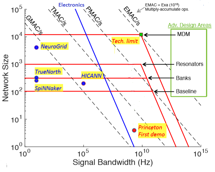
One fundamental limit on neural networks is the tradeoff between network size and the total signal bandwidth. As more neurons go on the network, it takes longer for information to transverse the network, either due to the speed of the network or some limit on how much information the network can transmit at any given time. Figure 1 demonstrates the current state of this trade-off in electronic and photonic systems. Even one of the faster electonic systems is bandwidth limited to 100kHz, with that limit decreasing as the network grows into multiple wafers due to inter-wafer communication delay [1]. In general, while electronic neural networks can contain tens of thousands of neurons, the slower speeds limit these networks to trillions of operations per second (TMAC/s) or slower. Photonic networks have the potential to break this barrier, without appreciably increasing network size.

Princeton recently demonstrated its first working physical photonic neural network, as shown in Figure 2, containing four neurons on different wavelengths [2]. The network utilizes a star topology, where the outputs of all the neurons enter the network at a single point, splitting off from that point to meet the weight banks. Each weight bank is a collection of Microring Resonators (MRR). Each MRR is tuned to a different wavelength, with an electric heater deforming the ring ever so slightly to adjust the actual percentage of light that couples through the ring, effectively applying a weight to that wavelength channel independent of other channels. This method for weighting each channel of a wavelength division multiplexed (WDM) signal has been the principal passive optical component in all Princeton Neural Network designs [3]. Once weighted, the addition occurs in a pair of balanced photodiodes, allowing for both positive and negative weights. The electric signal immediately goes to a Mach-Zehnder Modulator, whose non-linear properties act as the axon of the neuron itself. Each neuron modulates a different wavelength, and all wavelengths are multiplexed off-chip and fed back into the point of the star network.

Refer to caption
Figure 2: Princeton’s first photonic network demonstration.

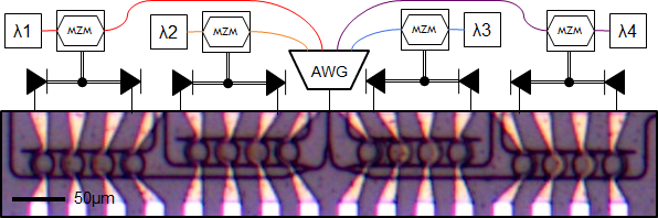
While Princeton’s demonstration is the first of its kind, it does suffer from some drawbacks. First of all, it is only four neurons large. The star topology has trouble scaling on-chip, due to the need for every point on the network to have a direct connection to the center of the star. Also, the large amount of off-chip fiber did slow the device into the kilohertz range, though that problem will not exist in a fully integrated system. Finally, in the long term, there are limits to both the channel selectivity of the microring resonators (channels per bandwidth) and the overall bandwidth of the waveguide, the product of which determines the total number of channels available in a network.

This work investigates the use of mode division multiplexing (MDM) to expand the information capacity of photonic neural networks by an order of magnitude.

1.2 Current Work in MDM

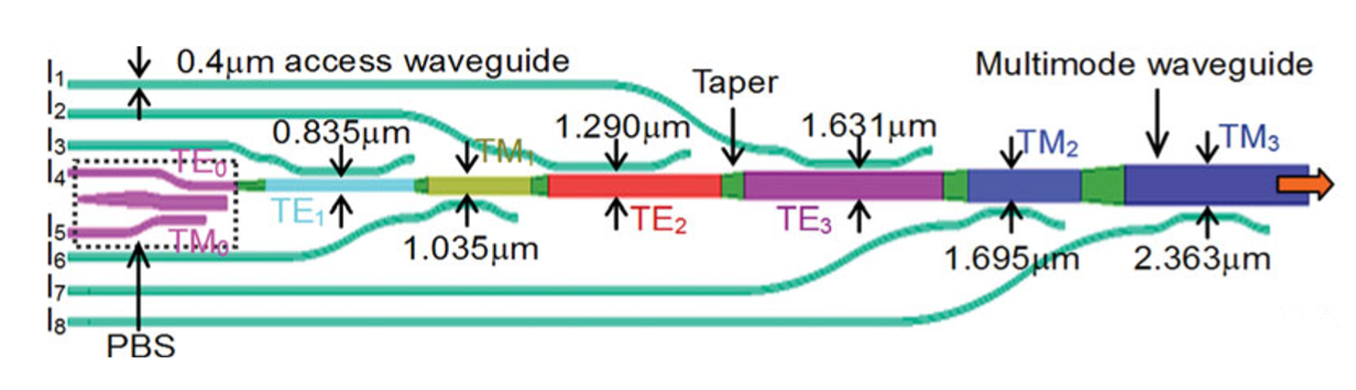
Previous work on MDM in silicon has focus solely on the actual multiplexer / demultiplexer. The general strategy is to couple signals on a single-mode waveguide to the highest order mode on a multi-mode waveguide, as shown in Figure 3 and demonstrated in silicon [4]. After each coupling portion for the Nth order mode, the bus waveguide adiabatically tapers larger to couple the (N+1)th order mode. The adiabatic taper, which occurs gradually, prevents any intermodal mixing between coupling. An exact mirror image of the device provides demultiplexing.

Refer to caption
Figure 3: Existing design for an on-chip mode (de)multiplexer [4]. Coupling occurs at asymmetric Y-junctions with varying bus widths.

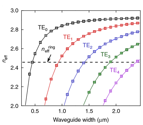
The principle behind the selectivity of the mode coupling is that the effective index in a waveguide for a given mode is dependent on the width, as shown in example simulation data in Figure 4 and demonstrated in silicon [5]. Optimal coupling occurs between two modes in two different waveguides when the effective indices match, and so if a given width is optimal for coupling to a given mode, it will be far from optimal for other modes. In practice, it is easiest to set the width of a multi-mode waveguide such that its highest order mode will couple to the single-mode MRR, as that mode already determines the minimum width of the waveguide, and then once that mode is coupled out, taper to the width for coupling with the next-highest-order mode.

Refer to caption
Figure 4: Example of simulated effective index data for waveguides of differing widths [5]. Optimal coupling occurs when the effective index of the multi-mode waveguide matches that of the single-mode MRR (example shown as dotted line).

2 Experiment 1: Waveguide Geometry

The goal of Experiment 1 is to determine the optimal coupling geometry between single- and multi-mode waveguides, since the value of the effective index differs by material and wavelength, and could diverge significantly from simulated data.

2.1 Experimental Design

Refer to caption
Figure 5: Asymmetric Mach-Zehnder Interferometer. The goal is to determine optimal waveguide width (W) and coupling length (L) for 100% coupling.

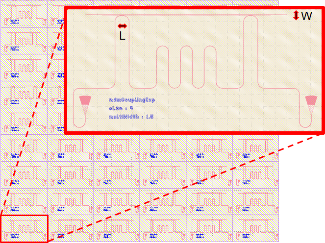
The design of this experiment is an asymmetric Mach-Zehnder interferometer. Given an input waveform Einsubscript𝐸𝑖𝑛E_{in}, the transfer function of the device can be written as:

[EoutEtaper]=M[Ein0]matrixsubscript𝐸𝑜𝑢𝑡subscript𝐸𝑡𝑎𝑝𝑒𝑟𝑀matrixsubscript𝐸𝑖𝑛0\begin{bmatrix}E_{out}\\ E_{taper}\\ \end{bmatrix}=M\begin{bmatrix}E_{in}\\ 0\\ \end{bmatrix} (1)

Where M is a composition of both single-mode to multi-mode couplers and a phase shift ΔϕΔitalic-ϕ\Delta\phi due to the difference in optical length of the two paths through the interferometer.

M=McouplerMΔϕMcoupler𝑀subscript𝑀𝑐𝑜𝑢𝑝𝑙𝑒𝑟subscript𝑀Δitalic-ϕsubscript𝑀𝑐𝑜𝑢𝑝𝑙𝑒𝑟M=M_{coupler}*M_{\Delta\phi}*M_{coupler} (2)

Mcouplersubscript𝑀𝑐𝑜𝑢𝑝𝑙𝑒𝑟M_{coupler} can be determined given a power coupling ratio α𝛼\alpha, conservation of energy, and a π2𝜋2\frac{\pi}{2} phase shift that occurs as power couples from one waveguide to another.

Mcoupler=[1αjαjα1α]subscript𝑀𝑐𝑜𝑢𝑝𝑙𝑒𝑟matrix1𝛼𝑗𝛼𝑗𝛼1𝛼M_{coupler}=\begin{bmatrix}\sqrt{1-\alpha}&j\sqrt{\alpha}\\ j\sqrt{\alpha}&\sqrt{1-\alpha}\\ \end{bmatrix} (3)

Combined with the phase shift Δϕ=kΔLΔitalic-ϕ𝑘Δ𝐿\Delta\phi=k*\Delta L, where k is the wavenumber related to the wavelength of the light, we can determine the transfer coefficient between the input waveform and the measured output:

M=[1αjαjα1α][ejkΔL001][1αjαjα1α]𝑀matrix1𝛼𝑗𝛼𝑗𝛼1𝛼matrixsuperscript𝑒𝑗𝑘Δ𝐿001matrix1𝛼𝑗𝛼𝑗𝛼1𝛼M=\begin{bmatrix}\sqrt{1-\alpha}&j\sqrt{\alpha}\\ j\sqrt{\alpha}&\sqrt{1-\alpha}\\ \end{bmatrix}\begin{bmatrix}e^{jk\Delta L}&0\\ 0&1\\ \end{bmatrix}\begin{bmatrix}\sqrt{1-\alpha}&j\sqrt{\alpha}\\ j\sqrt{\alpha}&\sqrt{1-\alpha}\\ \end{bmatrix} (4)
|EoutEin|2=|(1α)ejkΔLα|2=α2+(1α)22α(1α)cos(kΔL)superscriptsubscript𝐸𝑜𝑢𝑡subscript𝐸𝑖𝑛2superscript1𝛼superscript𝑒𝑗𝑘Δ𝐿𝛼2superscript𝛼2superscript1𝛼22𝛼1𝛼𝑐𝑜𝑠𝑘Δ𝐿\left\lvert\frac{E_{out}}{E_{in}}\right\rvert^{2}=\left\lvert(1-\alpha)e^{jk\Delta L}-\alpha\right\rvert^{2}=\alpha^{2}+(1-\alpha)^{2}-2\alpha(1-\alpha)cos(k\Delta L) (5)

Therefore, a power spectrogram of the device will result in a cosine with a DC-shift. The amplitude of that cosine, called the Extinction Ratio, is only dependent on the coupling ratio between the single-mode and multi-mode waveguides.

2.2 Simulations and Expected Results

Refer to caption
Figure 6: Simulation results for coupling between the fundamental mode (TE0𝑇subscript𝐸0TE_{0}) and the second order mode (TE2𝑇subscript𝐸2TE_{2}), for both the index-matched width (left) an a width mismatched by 20nm (right). Note that optical power oscillates back and forth between the waveguides over the course of one beat length. Below is a table of simulated index-matched widths and beat lengths for each mode.

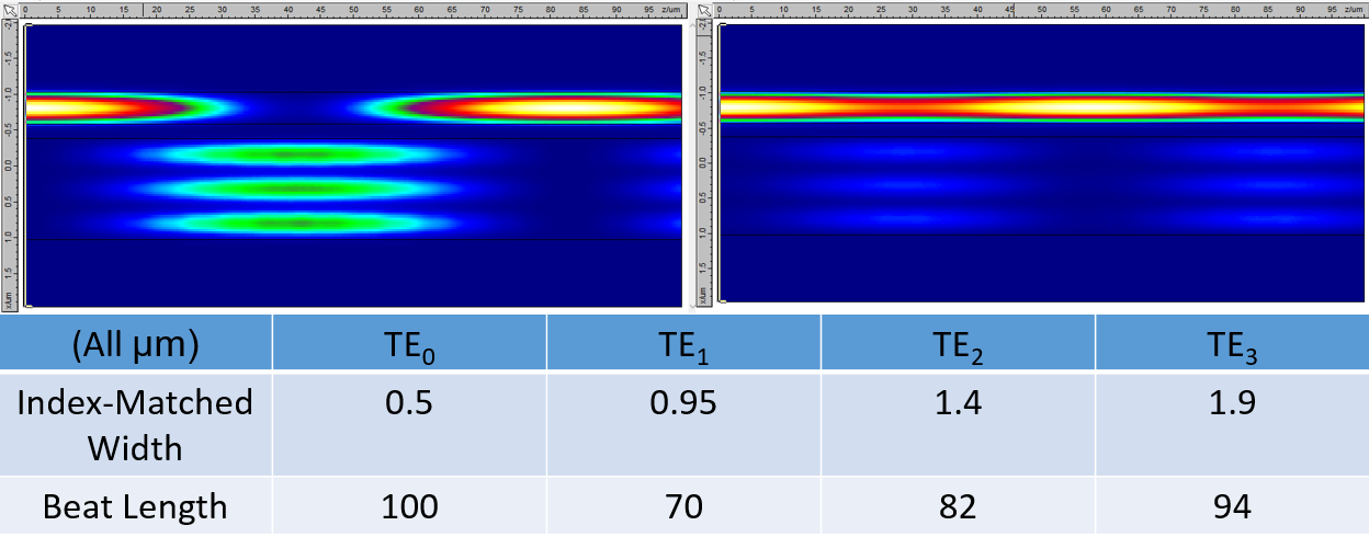
We can use simulations of optical coupling between single-mode and multi-mode waveguides to determine the relationship between W, L, and the coupling ratio α𝛼\alpha. Some of these results are presented in Figure 6. As shown previously, optimal coupling happens when the width of the multi-mode waveguide is such that the indices of refraction in the two waveguides match. Even a slight mismatch can drastically decrease the coupling ratio. Once the indices are matched, optical power oscillates back and forth between the two waveguides. The spacial period of this oscillation is called the beat length, and differs by mode. Optimal coupling occurs at half of the beat length, when all power has moved into the multi-mode waveguide.

α=f(W)(1cos(2πL(beatlength)))/2𝛼𝑓𝑊1𝑐𝑜𝑠2𝜋𝐿𝑏𝑒𝑎𝑡𝑙𝑒𝑛𝑔𝑡2\alpha=f(W)*(1-cos(2\pi\frac{L}{(beat\ length)}))/2 (6)

The first step in the experiment is to maximize the extinction ratio, which corresponds with α=12𝛼12\alpha=\frac{1}{2}. This implies that the width matches effective index and the coupling length is one-quarter or three-quarters of the beat length. The next step is to minimize the extinction ratio without changing the width. Since the extinction ratio is minimized with both α=1𝛼1\alpha=1 and α=0𝛼0\alpha=0, the simulation data can be used to help distinguish the two cases. It should be clear whether the coupling length is closer to the simulated beat length or the simulated half-beat length.

3 Experiment 2: Weight Bank

3.1 Experimental Design

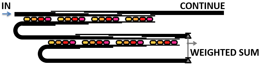
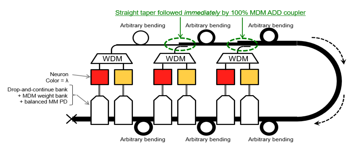
Using the simulated optimal coupling geometry, we designed a combined MDM / WDM weight bank to perform the weighted addition on the dendrite side of the neuron, as shown in Figure 7. The bank is composed of a series of stages, one per mode. Each stage is similar to th WDM weight bank from Princeton’s network demonstration: a series of MRRs tuned to each wavelength channel in the waveguide. Each MRR transmits a certain percentage of the optical power in its specific wavelength channel from the input bus into the ”drop” waveguide. The exact percentage is controlled by electric heaters that can slightly modify the exact perimeter of the MRR. The rest of the light in the channel is coupled completely into the ”add” waveguide. Finally, the input waveguide is adiabatically tapered down to the coupling width of the next-highest-order mode for the next stage, until the final stage has only a single-mode waveguide.

Refer to caption
Figure 7: (Top) Schematic for a four-mode four-wavelength MDM/WDM weight bank. (Bottom) Layout of the weight bank on-chip. Electric heaters are shown in blue.

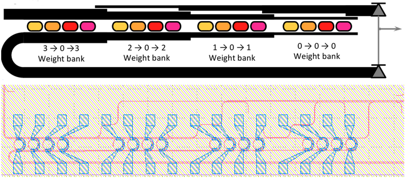
Both the ”add” and ”drop” waveguides are fed into two balanced photodiodes, which provides summation by converting the optical power into an electric current. The difference in current between the two photodiodes is the current that acts as the input for the neuron itself. The benefit of using the photodiode for summation is that it is mode- and wavelength-agnostic. Based on the mechanics of multi-mode coupling, each mode in the input gets coupled into a different mode of the ”add” waveguide, However, since the total optical power in that waveguide is still a correct weighted sum of each channel, the correct electrical current is drawn by the photodiode.

3.2 Intermodal Mixing

The summation in the photodiode also solves another issue with the weight bank: intermodal mixing. When there is a bend in a multi-mode waveguide, the mode basis changes throughout the course of the bend. The result is a shuffling of optical power between modes. Assuming no bending loss, this shuffling can be accurately modeled as a linear transformation with a unitary matrix.

[TE0TE1]=M[TE0TE1]matrix𝑇superscriptsubscript𝐸0𝑇superscriptsubscript𝐸1𝑀matrix𝑇subscript𝐸0𝑇subscript𝐸1\begin{bmatrix}TE_{0}^{\prime}\\ TE_{1}^{\prime}\\ \end{bmatrix}=M\begin{bmatrix}TE_{0}\\ TE_{1}\\ \end{bmatrix} (7)
MM=1superscript𝑀𝑀1M^{{\dagger}}M=1 (8)

Since the transformation is unitary, the total optical power in the waveguide does not change. Therefore, within the wavebank itself, the bend in the ”drop” waveguide makes no difference in the summation done by photodiode.

Refer to caption
Figure 8: (Top) Simulation of the fundamental mode of a two-mode waveguide going through a bend. The result is a mix of the fundamental and first-order mode. (Bottom) How a weight bank can undo the effects of an intermodal mixing matrix.

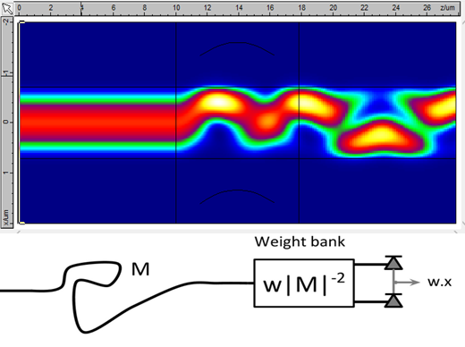
Closer inspection of Figure 7 would reveal that intermodal mixing also occurs outside of the weight bank in the form of a bending input waveguide. This could not be done in previous muilti-mode experiments, as there is no easy way to undo the mode mixing on chip through waveguide geometry alone. Both [4] and [5] use only straight multi-mode waveguides. Fortunately, a properly calibrated weight bank can be used to undo all intermodal mixing in the network. A weighted summation is mathematically equivalent to an inner product with a weighting vector:

y=w|x|2𝑦𝑤superscript𝑥2y=w\cdot\lvert x\rvert^{2} (9)

where |x|2superscript𝑥2\lvert x\rvert^{2} is the vector of optical power in each channel. If x is modified by a mix matrix |M|2superscript𝑀2\lvert M\rvert^{2}, then the same output can be preserved if w is modified by M’s inverse.

w|M|2|M|2|x|2=w|x|2=y𝑤superscript𝑀2superscript𝑀2superscript𝑥2𝑤superscript𝑥2𝑦w\lvert M\rvert^{-2}\cdot\lvert M\rvert^{2}\lvert x\rvert^{2}=w\cdot\lvert x\rvert^{2}=y (10)

By experimenting with known input vectors x and weights w, the individual components of M can be measured, allowing for the calibration of the weight bank. Calibrating each weight bank on the network allows for arbitrary bending in any multi-mode waveguide in the network, leading to more flexible network design and the ability to fit more neurons on a smaller surface area.

4 Experiment 3: Multi-Neuron Network

4.1 Experimental Design

The next step is to combine muiltiple weight banks into a full network, as shown in Figure 9. This design has two neurons on two channels on two different modes and one wavelength. Optical power is pumped into the network to the axons, which are just MRRs tied to electric heaters. Modulation of optical power via the electric heaters follows a Lorentzian function, providing the non-linear element that can act as a continuous (non-spiking) neuron. Each neuron uses the same wavelength of light, but couples onto a different mode in the main bus. The bus wraps around into a series of weight banks. The first bank cuts the power in half, while the subsequent weight banks provide the actual weighting before the light goes off-chip to be summed and fed back into the axons.

Refer to caption
Figure 9: Final CAD of a two-neuron network, including axons, one cascaded weight bank, and one non-cascaded weight bank.

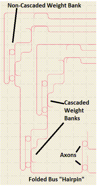
4.2 ”Hairpin” Topology and Cascaded Banks

As designed in Experiment 2, a weight bank has a single multi-mode input and two multi-mode outputs. To allow for multiple weight banks to share a single bus, and extra weight bank can be used with the sole purpose of dropping a fixed percentage of power from the shared bus before a second weight bank does the actual weighting. An example of these cascaded weight banks is shown in Figure 10. While the extra weight bank does flip the mode channels between the input and the continue waveguides, this can just be factored into the mode mixing matrix at the next cascaded weight bank. In Experiment 3, the first neuron uses a cascaded weight bank, while the second (and last) neuron in the network just uses a single weight bank.

Refer to caption
Figure 10: Schematic of a cascaded weight bank. The first bank drops a fixed percentage of power from the bus, while the second performs the actual weighted addition.

The actual layout of the network in Figure 9 is a folded bus, or ”hairpin,” topology. One limitation of the Princeton network demonstration is its limited ability to scale. Because every point in the star topology needs a direct connection to the source point, an addition of even one neuron can take up quite a bit of chip surface area. Furthermore, there is no easy way to split a multi-mode signal from one waveguide into multiple multi-mode waveguides. The hairpin topology places all axons on one side of the hairpin, and all dendrites on the other, as shown in Figure 11. Since there can be arbitrary waveguide bending between neurons, the hairpin can snake its way around the trip into an arbitrary configuration, allowing for flexible network and efficient use of chip surface area.

Refer to caption
Figure 11: Schematic of a folded bus, or ”hairpin,” network design. Arbitrary bending between neurons allows for a flexible on-chip network design.

5 Future Work and Applications

The silicon chip with these three experiments will be fabricated during the summer, and the resulting data should be sufficient to design a larger network of neurons for high speed computations.

5.1 Application: Digital Demixing

Refer to caption
Figure 12: Example of using a weight bank for channel selection. Multiple weight banks can completely demix all channels.

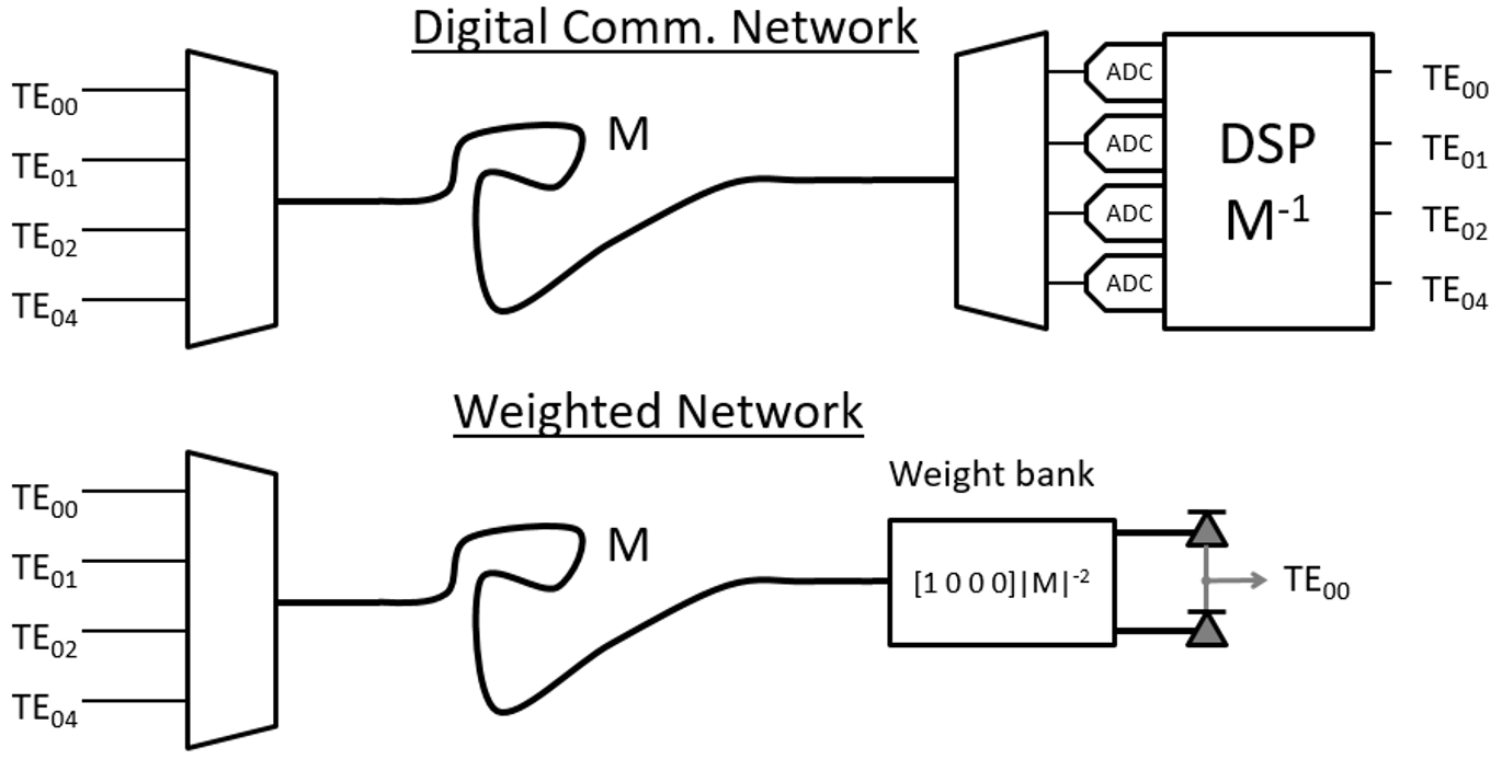
One application of the weight banks themselves is actually in digital applications. Multi-mode waveguides can greatly increase the aggregate bandwidth of digital optical systems on chip. However, intermodal mixing severely limits any bandwidth improvement, since DSP is required to invert the mixing matrix if there is any bending on chip. However, as shown in Figure 12, a single weight bank can be used to invert the mix matrix and select one of the mode channels. For N modes, N weight banks can be used in aggregate to completely invert the mixing matrix in the optical domain, without any DSP.

5.2 Application: RF Classification

Refer to caption
Figure 13: Examples of I-Q digital modulation schemes. With more dots in the diagram, more data can be sent per ”bit” interval.

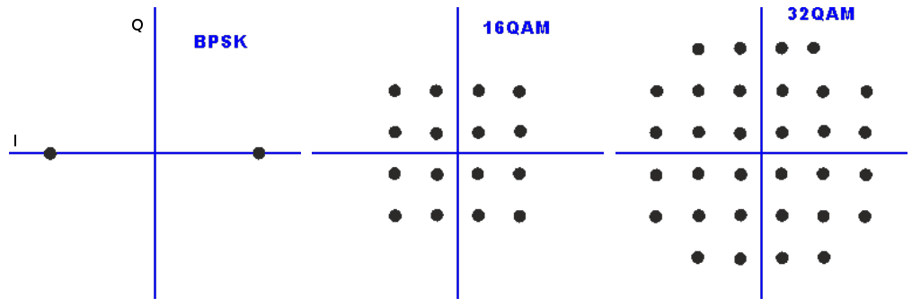
Finally, the full photonic neural network can be deployed for classification problems at Radio Frequencies. One practical example is modulation scheme classification. When broadcasting a signal over radio, one method of modulating digital data is to encode each bit as a combination of the amplitude of a cosine, the in-phase or I component, and the amplitude of a sin, the quadrature or Q component.

Y(t)=I(t)cos(ωt)+Q(t)sin(ωt)𝑌𝑡𝐼𝑡𝑐𝑜𝑠𝜔𝑡𝑄𝑡𝑠𝑖𝑛𝜔𝑡Y(t)=I(t)cos(\omega t)+Q(t)sin(\omega t) (11)

Examples of such schemes are shown in Figure 13. A photonic neural network could take as inputs two analog parameters I(t)𝐼𝑡I(t) and Q(t)𝑄𝑡Q(t), and output its best guess as to the modulation scheme in real time. Combined with flexible, software-defined radio, such networks could be used to sweep large swaths of the radio spectrum searching for data channels.

Photonic neural networks have the potential to be a driving force in high speed processing and computing. MDM can become a vital component in drastically increasing network size and aggregate bandwidth, allowing for more complex applications in the future.

References

  • [1] J. Schemmel, et al., ”Wafer-scale integration of analog neural networks,” in IEEE Int. Joint Conf. on Neural Networks, Hong Kong, 2008, pp. 431-438.
  • [2] A. Tait, et al., ”Demonstration of a silicon photonic neural network,” Submitted, Pending Publication, 2016.
  • [3] A. Tait, et al., ”Continuous control of microring weight banks,” in IEEE Photonics Conf., Reston, VA, 2015, pp. 411-412.
  • [4] J. Wang, et al., ”On-chip silicon 8-channel hybrid (de)multiplexer enabling simultaneous mode- and polarization-division-multiplexing,” Laser & Photonics Reviews, rev. 8, no. 2, Wiley-VCH GmbH & Co. KGaA, Weinheim, 2014.
  • [5] L. Luo, et al., ”WDM-compatible mode-division multiplexing on silicon chip,” Nature Communications, vol. 5, no. 3069, Macmillian Publishers Limited, 2014.

6 Code Appendix

The on-chip layout of each experiment was procedurally generated using MATLAB.

6.1 Project Definitions

1% MainProject
2% Author : Ethan
3
4clear; close all; clc; format long; format compact;
5% clear classes; % this also clears breakpoints, so no bueno
6
7% Get to the right directory
8thisFile = mfilename(’fullpath’);
9thisDir = thisFile(1:end-length(mfilename));
10cd(thisDir);
11
12% Make sure the right paths are added, and other project paths are removed
13tp = cd; cd(’../Functions - AlexUtil’);
14makePaths(tp);
15
16% Project meta data
17cad = struct(’author’, ’Ethan’, % project lead author or company
18 ’fab’, ’UBC’, % fabrication facility
19 ’process’, ’Ebeam’, % fabrication process
20 ’run’, ’06’, % run name
21 ’name’, ’MDMCoupling’, % project name
22 ’layermap’, ’UBC_map’, % layer map name
23 ’uunit’, 1e-6, % CAD scale (1e-6 - > microns)
24 ’dbunit’, 1e-9, % CAD database unit (1e-9 - > nm)
25 ’size’, [10000, 10000], % Floorplan dimensions
26 ’margin’, struct(’left’, 100, ’right’, 100, ’top’, 100, ’bottom’, 100), % safety margin
27 ’v’, ’v1’); % version number
28save(’cadMeta.mat’,’cad’);
29
30%% —– chip-wide variables ——-
31itPerRow = 4;
32itStart = 0;
33wgBias = 0.0;
34
35% Default experiment information
36defaultExp = struct(’name’,’defaultName’,
37 ’deviceModel’, @device_blank,
38 ’setBuilder’, @buildSet_arrayed,
39 ’buildInfo’, struct(’approAli’,’top’,’approSp’,’wg’,’approBend’,10),
40 ’fixedArgs’, {0},
41 ’pInfo’, struct(’name’,’null’,’val’,0,’axis’,’x’),
42 ’gc’, struct(’ref’,’TE1550_SubGC_neg31_oxide_hooked’,’flip’,-1,’sp’,127,’nPer’,2), %no longer supports parameters, use references
43 ’wg’, Waveguide(.5+wgBias,[1;0],10,10),
44 ’thermal’,Wire(4,[11;0],10,20),
45 ’intercon’,Wire(5,[12;0],10,20),
46 ’contactInfo’,{0},
47 ’rect’, [200,500],
48 ’offs’, [0,0]);
49defaultExp.contactInfo = {[]};
50defaultExp.fixedArgs = {[]};
51
52contCounter = 0;
53
54% ————————
55%% Describe cell mdmCouplingExp
56% ————————
57someRads = [(.5:.5:5),(6:13)]; %[1,2,4,8,15];
58pInfoModBend(1) = struct(’name’, ’cLen’,
59 ’val’, [0,1,2,3,4,5,10,15,20],
60 ’axis’,’y’);
61pInfoModBend(2) = struct(’name’, ’multiWidth’,
62 ’val’, someRads(1:1),
63 ’axis’,’x’);
64
65mdmCouplingExp = ReadOptions(defaultExp,’name’,’mdmCouplingExp’,
66 ’pInfo’,pInfoModBend,
67 ’deviceModel’,@device_MultiInterferometer,
68 ’setBuilder’,@buildExpSet_modular_duo,
69 ’thermal’,[],
70 ’rect’,[460,260]);
71
72% ————————
73%% Describe cell mdmWeightBankExp
74% ————————
75
76numModes = 4;
77numWL = 4;
78
79mrr = Microring(.2,defaultExp.wg.layer,defaultExp.wg.dtype,’w’,.5,’radius’,10,’straightLength’,2);
80fb = FilterBank_v2(defaultExp.wg,defaultExp.thermal,mrr,’orderN’,numWL,’dL’,0.1,’busHold’,8);
81
82multiDeviceModel = @device_MDMWeightBank;
83
84dParams = [numModes, numWL];
85
86mdmWeightBankExp = ReadOptions(defaultExp,’name’,’mdmWeightBankExp’,
87 ’deviceModel’,@device_ModeMUXArr,
88 ’contactInfo’,{1},
89 ’thermal’,ReadOptions(defaultExp.thermal,’l1pad’,18),
90 ’intercon’,ReadOptions(defaultExp.intercon,’l1pad’,18),
91 ’gc’,ReadOptions(defaultExp.gc,’flip’,-1, ’nPer’, numModes * 3),
92 ’fixedArgs’,{multiDeviceModel, dParams, fb}, % Multi-Mode Modular Device Model and Parameters
93 ’rect’,[400,1000]);
94
95% ————————
96%% Describe cell mdmWeightBankSafeExp
97% ————————
98
99numModes = 4;
100numWL = 4;
101
102fb2 = fb.copy;
103fb2.orderN = numWL;
104fb2.recalculate();
105
106multiDeviceModel = @device_MDMWeightBankSafe;
107
108dParams = [numModes, numWL];
109
110mdmWeightBankSafeExp = ReadOptions(defaultExp,’name’,’mdmWeightBankSafeExp’,
111 ’deviceModel’,@device_ModeMUXArrSafe,
112 ’contactInfo’,{2},
113 ’thermal’,ReadOptions(defaultExp.thermal,’l1pad’,18),
114 ’intercon’,ReadOptions(defaultExp.intercon,’l1pad’,18),
115 ’gc’,ReadOptions(defaultExp.gc,’flip’,-1, ’nPer’, numModes * 3),
116 ’fixedArgs’,{multiDeviceModel, dParams, fb2}, % Multi-Mode Modular Device Model and Parameters
117 ’rect’,[400,1000]);
118
119% ————————
120%% Describe cell busNtwrkExp
121% ————————
122
123numModesNet = 2;
124numWLNet = 1;
125
126multiDeviceModelNet = @device_MDMWeightBank;
127
128dParamsNet = [numModesNet, numWLNet];
129
130busNtwrkExp = ReadOptions(defaultExp,’name’,’busNtwrkExp’,
131 ’deviceModel’,@device_NtwrkArr,
132 ’gc’,ReadOptions(defaultExp.gc,’flip’,-1, ’nPer’, 5*numModesNet),
133 ’fixedArgs’,{multiDeviceModelNet, dParamsNet}, % Multi-Mode Modular Device Model and Parameters
134 ’rect’,[400,1000]);
135
136% ————————
137%% Describe cell busNtwrkInvExp
138% ————————
139numModesNet = 4;
140numWLNet = 4;
141
142multiDeviceModelNet = @device_MDMWeightBank;
143
144dParamsNet = [numModesNet, numWLNet];
145
146fb3 = fb2.copy;
147fb3.orderN = numWLNet;
148fb3.recalculate();
149
150busNtwrkInvExp = ReadOptions(busNtwrkExp,’name’,’busNtwrkInvExp’,
151 ’contactInfo’,{3},
152 ’thermal’,ReadOptions(defaultExp.thermal,’l1pad’,18),
153 ’intercon’,ReadOptions(defaultExp.intercon,’l1pad’,18),
154 ’gc’,ReadOptions(defaultExp.gc,’flip’,-1, ’nPer’, 5*numModesNet),
155 ’fixedArgs’,{multiDeviceModelNet, dParamsNet, fb3, -1}, % Multi-Mode Modular Device Model and Parameters
156 ’deviceModel’,@device_NtwrkArrInverted,
157 ’rect’,[400,1000]);
158
159% ————————
160%% Describe cell busNtwrkWDMExp
161% ————————
162numModesNet = 1;
163numWLNet = 4;
164
165multiDeviceModelNet = @device_MDMWeightBank;
166
167dParamsNet = [numModesNet, numWLNet];
168
169fb4 = fb2.copy;
170fb4.orderN = numWLNet;
171fb4.recalculate();
172
173busNtwrkWDMExp = ReadOptions(busNtwrkInvExp,’name’,’busNtwrkWDMExp’,
174 ’contactInfo’,{4},
175 ’gc’,ReadOptions(defaultExp.gc,’flip’,-1, ’nPer’, 5*numModesNet),
176 ’fixedArgs’,{multiDeviceModelNet, dParamsNet, fb4, -1}, % Multi-Mode Modular Device Model and Parameters
177 ’rect’,[400,1000]);
178
179
180%% Put the experiment options in an array (comment them to suppress)
181expArray = mdmCouplingExp;
182expArray(end+1) = mdmWeightBankExp;
183expArray(end+1) = mdmWeightBankSafeExp;
184expArray(end+1) = busNtwrkExp;
185expArray(end+1) = busNtwrkWDMExp;
186expArray(end+1) = busNtwrkInvExp;
187
188
189% Define how they are put together in the topcell
190% Currently, just a name is needed
191mirrorNets = ones(1,contCounter);
192multiInfo = struct(’name’,’topcell’,
193 ’putNextTo’,{{’mdmCouplingExp’,’mdmWeightBankExp’}},
194 ’rotate’,{{’busNtwrkExp’}},
195 ’L1netMirror’,mirrorNets,
196 ’centering’,false);
197
198%createMasterHDFfromTypes(’mytestfile.h5’,expArray);
199hdfFilename = [cad.name, ’.h5’];
200%hdfFilename = [];
201
202% call functions to build all GDS files
203delete(’./*.gds’); delete(’./Cells/*’);
204buildInfo = BuildCellsFromInfo(expArray,hdfFilename);
205BuildMultiCell(buildInfo, multiInfo);
206addpath(’./Cells’);
207
208sprintf(’Merging final files. If it crashes, <a href=”matlab: opentoline(%s,25)”>go here</a>!’, which(’MergeGDS.m’))
209MergeCells;
210delete(’cadMeta.mat’);

6.2 Mach-Zehnder Interferometer

1%% device_MultiInterferometer
2% Author : Ethan
3% param format: [coupling length; multi-mode fiber width]
4function [topcell, infoOut] = device_MultiInterferometer(topcell, infoOut, phW, len, param)
5
6% Fetch Parameters
7cLen = param(1);
8mmWidth = param(2);
9
10% Constants (um)
11taperLen = 50;
12arcLen = 10;
13vertSep = 100;
14interLen = 120;
15
16cplSep = 0.5;
17
18% Length Check
19minLen = 2*taperLen + 2*cLen + 8*arcLen + interLen;
20if len < minLen
21 [topcell,infoOut] = PlaceRect(topcell,infoOut,len,phW.w,phW.layer,phW.dtype);
22 return
23end
24
25% Calculate Padding
26padLen = (len - minLen) / 2.0;
27
28% Approach
29[topcell,infoOut] = PlaceRect(topcell,infoOut,taperLen,phW.w,phW.layer,phW.dtype);
30[topcell, infoOut] = PlaceArc(topcell, infoOut, 90, arcLen, phW.w, phW.layer, phW.dtype);
31[topcell,infoOut] = PlaceRect(topcell,infoOut,vertSep,phW.w,phW.layer,phW.dtype);
32[topcell, infoOut] = PlaceArc(topcell, infoOut, -90, arcLen, phW.w, phW.layer, phW.dtype);
33
34%%% Multi-Mode Fiber %%%
35infoOutMM = infoOut;
36if infoOutMM.ori == 0
37 infoOutMM.pos(2) = infoOut.pos(2) + phW.w / 2.0 + cplSep + mmWidth / 2.0;
38 infoOutMM.pos(1) = infoOut.pos(1) - arcLen - taperLen;
39end
40if infoOutMM.ori == -90
41 infoOutMM.pos(2) = infoOut.pos(2) + arcLen + taperLen;
42 infoOutMM.pos(1) = infoOut.pos(1) + phW.w / 2.0 + cplSep + mmWidth / 2.0;
43end
44
45[topcell,infoOutMM] = PlaceRect(topcell,infoOutMM,taperLen,0.001,phW.layer,phW.dtype, ’endwidth’, mmWidth);
46[topcell,infoOutMM] = PlaceRect(topcell,infoOutMM,6*arcLen + 2*cLen + 2*padLen + interLen,mmWidth,phW.layer,phW.dtype);
47[topcell,~] = PlaceRect(topcell,infoOutMM,taperLen,mmWidth,phW.layer,phW.dtype, ’endwidth’, 0.001);
48
49%%% End Multi-Mode Fiber %%%
50
51% Coupler
52[topcell,infoOut] = PlaceRect(topcell,infoOut,cLen,phW.w,phW.layer,phW.dtype);
53
54% Detatch
55[topcell, infoOut] = PlaceArc(topcell, infoOut, -90, arcLen, phW.w, phW.layer, phW.dtype);
56[topcell,infoOut] = PlaceRect(topcell,infoOut,vertSep,phW.w,phW.layer,phW.dtype);
57[topcell, infoOut] = PlaceArc(topcell, infoOut, 90, arcLen, phW.w, phW.layer, phW.dtype);
58
59% Padding and Interleaver
60[topcell,infoOut] = PlaceRect(topcell,infoOut,padLen,phW.w,phW.layer,phW.dtype);
61for i = 1:3
62 [topcell, infoOut] = PlaceArc(topcell, infoOut, 90, arcLen, phW.w, phW.layer, phW.dtype);
63 [topcell,infoOut] = PlaceRect(topcell,infoOut,vertSep/2,phW.w,phW.layer,phW.dtype);
64 [topcell, infoOut] = PlaceArc(topcell, infoOut, -90, arcLen, phW.w, phW.layer, phW.dtype);
65 [topcell, infoOut] = PlaceArc(topcell, infoOut, -90, arcLen, phW.w, phW.layer, phW.dtype);
66 [topcell,infoOut] = PlaceRect(topcell,infoOut,vertSep/2,phW.w,phW.layer,phW.dtype);
67 [topcell, infoOut] = PlaceArc(topcell, infoOut, 90, arcLen, phW.w, phW.layer, phW.dtype);
68end
69[topcell,infoOut] = PlaceRect(topcell,infoOut,padLen,phW.w,phW.layer,phW.dtype);
70
71% Second Approach
72[topcell, infoOut] = PlaceArc(topcell, infoOut, 90, arcLen, phW.w, phW.layer, phW.dtype);
73[topcell,infoOut] = PlaceRect(topcell,infoOut,vertSep,phW.w,phW.layer,phW.dtype);
74[topcell, infoOut] = PlaceArc(topcell, infoOut, -90, arcLen, phW.w, phW.layer, phW.dtype);
75
76% Second Coupler
77[topcell,infoOut] = PlaceRect(topcell,infoOut,cLen,phW.w,phW.layer,phW.dtype);
78
79% Second Detatch
80[topcell, infoOut] = PlaceArc(topcell, infoOut, -90, arcLen, phW.w, phW.layer, phW.dtype);
81[topcell,infoOut] = PlaceRect(topcell,infoOut,vertSep,phW.w,phW.layer,phW.dtype);
82[topcell, infoOut] = PlaceArc(topcell, infoOut, 90, arcLen, phW.w, phW.layer, phW.dtype);
83[topcell,infoOut] = PlaceRect(topcell,infoOut,taperLen,phW.w,phW.layer,phW.dtype);
84
85end

6.3 MDM/WDM Weight Bank

1%% device_MDMWeightBank
2% Author : Ethan
3% param format: [coupling length; multi-mode fiber width]
4function [topcell, infoOut, infoMetalOut] = device_MDMWeightBank(topcell, infoIn, phW, MeT, param, varargin)
5infoMetalOut = {};
6
7% Fetch Parameters
8numModes = param(1);
9
10mdmFile = matfile(’../Functions - AlexUtil/MDMparams.mat’,’Writable’,false);
11mmWids = mdmFile.wuse;
12taperLen = mdmFile.taper;
13
14% Get a filter bank, or make one
15if isempty(varargin)
16 numWL = param(2);
17 mrr = Microring(.2,phW.layer,phW.dtype,’w’,mmWids(1),’radius’,phW.r,’straightLength’,2);
18 fbObj = FilterBank_v2(Waveguide(.5,[1;0],10,10),Wire(4,[11;0],10,20),mrr,’orderN’,numWL,’dL’,.1,’busHold’,8);
19else
20 fbObj = varargin{1};
21end
22
23% Is it hooked on the drop port
24if length(varargin) < 2
25 ishooked = 2;
26else
27 ishooked = varargin{2};
28end
29
30if length(varargin) < 3
31 side = 1;
32else
33 side = varargin{3};
34end
35
36
37% Draw Approach
38[topcell,infoIn] = PlaceRect(topcell, infoIn, phW.r, mmWids(numModes), phW.layer, phW.dtype);
39
40% Draw Filter Bank
41n = numModes;
42infoThru = infoIn;
43infoOut = 0;
44mmWids(end+1) = mmWids(end);
45%radius = 10;
46
47prevInfoCross = [];
48
49while n > 0
50
51 % WDM Filter
52 fbObj.busWGwidth = [mmWids(n); mmWids(n)];
53 fbObj.meT = MeT;
54 fbObj.recalculate();
55 [topcell, infoThru, infoCross, infoContra, infoMet] = fbObj.place(topcell,infoThru,’side’,side);
56 if n == numModes
57 infoWrap = infoContra;
58 end
59
60 % Draw Drop Demux, or if it’s the last one draw a terminator
61 if n > 1
62 demux = ModeMUX(phW,[n,n-1,side]);
63 [topcell, infoThru, ~] = demux.place(topcell, infoThru, side);
64 else
65 % Kill taper
66 [topcell, ~] = PlaceRect(topcell, infoCross, taperLen, mmWids(1), phW.layer, phW.dtype,’endwidth’,0.01);
67 end
68
69 % Draw Add Mux
70 if n == numModes && numModes > 1
71 magic1 = 30;
72 infoMuxOut = SplitInfo(infoThru, 1);
73 [topcell,infoMuxOut] = PlaceArc(topcell, infoMuxOut, -90*side, phW.r, phW.w, phW.layer, phW.dtype);
74 [topcell,infoMuxOut] = PlaceRect(topcell, infoMuxOut, magic1, phW.w, phW.layer, phW.dtype);
75 [topcell,infoOut] = PlaceArc(topcell, infoMuxOut, 90*side, phW.r, phW.w, phW.layer, phW.dtype);
76 elseif numModes > 1
77 if n > 1
78 infoMuxOut = SplitInfo(infoThru, 1);
79 else
80 infoMuxOut = infoThru;
81 end
82 [topcell,infoOut] = PlaceRect(topcell, infoOut, abs(infoOut.pos(2) - infoMuxOut.pos(2)), mmWids(numModes-n), phW.layer, phW.dtype);
83 mux = ModeMUX(phW, [numModes - n, numModes - n + 1, -side]);
84 combInfo = MergeInfo(infoOut, infoMuxOut);
85 if side == -1, combInfo.pos = flipud(combInfo.pos); end
86 [topcell, infoOut] = mux.place(topcell, combInfo);
87 else
88 infoMuxOut = infoThru;
89 [topcell,infoOut] = PlaceRect(topcell, infoMuxOut, taperLen + phW.sp, mmWids(1), phW.layer, phW.dtype);
90 end
91
92 if n < numModes
93 % Connect infoContra and PrevInfoCross
94 [topcell, ~] = PlaceSBend(topcell, prevInfoCross, abs(prevInfoCross.pos(2) - infoContra.pos(2)), infoContra.pos(1) - prevInfoCross.pos(1), phW.r, mmWids(n), phW.layer, phW.dtype);
95 end
96
97 % Draw Taper, new previnfocross
98 if n > 1
99 infoThru = SplitInfo(infoThru, 2);
100 [topcell, prevInfoCross] = PlaceRect(topcell, infoCross, taperLen, mmWids(n), phW.layer, phW.dtype,’endwidth’,mmWids(n-1));
101 end
102
103 % Accumulate metals
104 if isempty(infoMetalOut)
105 infoMetalOut = infoMet;
106 elseif ~isempty(infoMetalOut{1}) && ~isempty(infoMet{1})
107 infoMetalOut = {MergeInfo(infoMetalOut{1},infoMet{1}), MergeInfo(infoMetalOut{2},infoMet{2})};
108 end
109
110 n = n - 1;
111end
112
113% Draw Drop Wrap-Around
114if ishooked > 0
115 [topcell,infoWrap] = PlaceArc(topcell, infoWrap, -180*side, phW.r, mmWids(numModes), phW.layer, phW.dtype);
116end
117if ishooked > 1
118 [topcell,infoWrap] = PlaceRect(topcell, infoWrap, abs(infoWrap.pos(2) - infoOut.pos(2)), mmWids(numModes), phW.layer, phW.dtype);
119end
120
121infoOut = MergeInfo(infoOut, infoWrap);
122
123
124end

6.4 Folded Bus Network

1%% device_NtwrkArr
2% Author : Ethan
3
4% Dummy device for modular type experiments (which require a certain len)
5% See device_blank for arrayed type experiments
6function [topcell, infoAll, infoMetalOut, refs] = device_NtwrkArr(topcell, infoAll, phW, MeT, params, varargin)
7infoMetalOut = [];
8refs = [];
9deviceModel = varargin{1};
10dParams = varargin{2};
11numModes = dParams(1);
12ioNum = size(infoAll.pos,1);
13
14% Import Params
15mdmFile = matfile(’../Functions - AlexUtil/MDMparams.mat’,’Writable’,false);
16mmWids = mdmFile.wuse;
17taperLen = mdmFile.taper;
18
19% Get a microring, or make one
20if isempty(varargin)
21 %numWL = param(2);
22 mrrObj = Microring(.2,phW.layer,phW.dtype,’w’,mmWids(1),’radius’,phW.r,’straightLength’,2);
23else
24 mrrObj = varargin{1};
25end
26
27% Construct Demux
28demux = ModeMUX(phW,[numModes,1,1]);
29
30% Draw Modulator
31mrr = Microring(.2,1,0,’w’,mmWids(1),’radius’,10,’straightLength’,2);
32fb = FilterBank_v2(Waveguide(.5,[1;0],10,10),Wire(4,[11;0],10,20),mrr,’orderN’,1,’dL’,.1,’busHold’,8);
33fb.busWGwidth = [mmWids(1); mmWids(1)];
34fb.meT = MeT;
35fb.recalculate();
36
37n = numModes;
38prevInfoCross = [];
39while n > 0
40 fbObj = fb.copy();
41
42 infoPwr = SplitInfo(infoAll, ioNum-numModes+n);
43
44 % Approach
45 [topcell,infoPwr] = PlaceRect(topcell, infoPwr, taperLen, mmWids(1), phW.layer, phW.dtype);
46 [topcell,infoPwr] = PlaceArc(topcell, infoPwr, -90, phW.r, mmWids(1), phW.layer, phW.dtype);
47
48 % Modulator
49 fbObj.busWGwidth = [mmWids(1); mmWids(n)];
50 fbObj.recalculate();
51
52 [topcell, infoThru, infoCross, infoContra, ~] = fbObj.place(topcell,infoPwr,’side’,1);
53
54 % Kill Taper
55 [topcell, ~] = PlaceRect(topcell, infoThru, taperLen, mmWids(1), phW.layer, phW.dtype,’endwidth’,0.01);
56
57 if n > 1
58 % Adiabatic Taper
59 [topcell, prevInfoCross] = PlaceRect(topcell, infoCross, taperLen, mmWids(n), phW.layer, phW.dtype,’endwidth’,mmWids(n-1));
60 end
61
62 if n < numModes
63 % S bend to meet taper
64 [topcell, ~] = PlaceSBend(topcell, infoContra, abs(prevInfoCross.pos(2) - infoContra.pos(2)), infoContra.pos(1) - prevInfoCross.pos(1), phW.r, mmWids(n), phW.layer, phW.dtype);
65 else
66 % Contra is Output!
67 infoOut = infoContra;
68 end
69
70 n = n - 1;
71end
72
73% Draw Hairpin to Dendrites
74[topcell, infoOut] = PlaceArc(topcell, infoOut, -90, phW.r, mmWids(numModes), phW.layer, phW.dtype);
75[topcell, infoOut] = PlaceRect(topcell, infoOut, taperLen * 5, mmWids(numModes), phW.layer, phW.dtype);
76[topcell, infoOut] = PlaceArc(topcell, infoOut, -90, phW.r, mmWids(numModes), phW.layer, phW.dtype);
77
78% Draw Drop / Continue
79[topcell, infoOut] = deviceModel(topcell, infoOut, phW, MeT, dParams);
80
81infoWB = SplitInfo(infoOut, 1);
82
83infoCont = SplitInfo(infoOut, 2);
84
85% Draw Weight Bank 1
86[topcell, infoOut] = deviceModel(topcell, infoWB, phW, MeT, dParams);
87infoMid = SplitInfo(infoOut, 1);
88infoBot = SplitInfo(infoOut, 2);
89
90% Place Unapproach
91[topcell, infoMid] = PlaceArc(topcell, infoMid, -90, phW.r, mmWids(numModes), phW.layer, phW.dtype);
92
93[topcell, infoBot] = PlaceRect(topcell, infoBot, 50, mmWids(numModes), phW.layer, phW.dtype);
94[topcell, infoBot] = PlaceArc(topcell, infoBot, -90, phW.r, mmWids(numModes), phW.layer, phW.dtype);
95[topcell, infoBot] = PlaceRect(topcell, infoBot, infoBot.pos(1) - infoMid.pos(1), mmWids(numModes), phW.layer, phW.dtype);
96
97
98% Place Demux
99[topcell, infoMid] = demux.place(topcell, infoMid);
100[topcell, infoBot] = demux.place(topcell, infoBot);
101
102infoComb = MergeInfo(infoMid, infoBot);
103
104% Align Outputs
105
106infoNewComb = 0;
107for n = 1:2*numModes
108 infoTest = SplitInfo(infoComb, n);
109 [topcell, infoTest] = PlaceRect(topcell, infoTest, infoTest.pos(1) - infoAll.pos(1, 1), phW.w, phW.layer, phW.dtype);
110 if isstruct(infoNewComb)
111 infoNewComb = MergeInfo(infoNewComb, infoTest);
112 else
113 infoNewComb = infoTest;
114 end
115end
116
117% Draw Weight Bank 2
118[topcell, infoCont] = PlaceRect(topcell, infoCont, 100, mmWids(numModes), phW.layer, phW.dtype);
119[topcell, infoCont] = PlaceArc(topcell, infoCont, 90, phW.r, mmWids(numModes), phW.layer, phW.dtype);
120[topcell, infoCont] = PlaceArc(topcell, infoCont, -90, phW.r, mmWids(numModes), phW.layer, phW.dtype);
121[topcell, infoOut] = deviceModel(topcell, infoCont, phW, MeT, dParams);
122infoMid = SplitInfo(infoOut, 1);
123infoBot = SplitInfo(infoOut, 2);
124
125% Place Unapproach
126[topcell, infoMid] = PlaceArc(topcell, infoMid, -90, phW.r, mmWids(numModes), phW.layer, phW.dtype);
127
128[topcell, infoBot] = PlaceRect(topcell, infoBot, 50, mmWids(numModes), phW.layer, phW.dtype);
129[topcell, infoBot] = PlaceArc(topcell, infoBot, -90, phW.r, mmWids(numModes), phW.layer, phW.dtype);
130[topcell, infoBot] = PlaceRect(topcell, infoBot, infoBot.pos(1) - infoMid.pos(1), mmWids(numModes), phW.layer, phW.dtype);
131
132
133% Place Demux
134[topcell, infoMid] = demux.place(topcell, infoMid);
135[topcell, infoBot] = demux.place(topcell, infoBot);
136
137infoComb = MergeInfo(infoMid, infoBot);
138
139% Align Outputs
140
141infoNewComb2 = 0;
142for n = 1:2*numModes
143 infoTest = SplitInfo(infoComb, n);
144 [topcell, infoTest] = PlaceRect(topcell, infoTest, infoTest.pos(1) - infoAll.pos(1, 1), phW.w, phW.layer, phW.dtype);
145 if isstruct(infoNewComb2)
146 infoNewComb2 = MergeInfo(infoNewComb2, infoTest);
147 else
148 infoNewComb2 = infoTest;
149 end
150end
151
152% Finalize
153infoNewComb2 = MergeInfo(infoNewComb, infoNewComb2);
154infoTop = SplitInfo(infoAll, (ioNum - numModes + 1):ioNum );
155infoAll = MergeInfo(infoTop, infoNewComb2);
156end