Cathodoluminescence-based
nanoscopic thermometry
in a lanthanide-doped phosphor
Chem] Department of Chemistry, University of California at Berkeley \alsoaffiliation[Stanford] Department of Bioengineering, Stanford University (present address) Mech] Department of Mechanical Engineering, University of California at Berkeley MF] Molecular Foundry, Lawrence Berkeley National Laboratory Chem] Department of Chemistry, University of California at Berkeley Atto] Attolight AG, EPFL Innovation Park D, 1015 Lausanne, Switzerland MF] Molecular Foundry, Lawrence Berkeley National Laboratory MF] Molecular Foundry, Lawrence Berkeley National Laboratory MF] Molecular Foundry, Lawrence Berkeley National Laboratory Mech] Department of Mechanical Engineering, University of California at Berkeley Chem] Department of Chemistry, University of California at Berkeley \alsoaffiliation[Phys] Department of Physics, University of California at Berkeley \alsoaffiliation[Biop] Molecular Biophysics and Integrative Bioimaging Division, Lawrence Berkeley National Laboratory \alsoaffiliation[Kav] Kavli Energy NanoScience Institute, Berkeley
Crucial to analyze phenomena as varied as plasmonic hot spots and the spread of cancer in living tissue, nanoscale thermometry is challenging: probes are usually larger than the sample under study, and contact techniques may alter the sample temperature itself. Many photostable nanomaterials whose luminescence is temperature-dependent, such as lanthanide-doped phosphors, have been shown to be good non-contact thermometric sensors when optically excited. Using such nanomaterials, in this work we accomplished the key milestone of enabling far-field thermometry with a spatial resolution that is not diffraction-limited at readout.
We explore thermal effects on the cathodoluminescence of lanthanide-doped NaYF4 nanoparticles. Whereas cathodoluminescence from such lanthanide-doped nanomaterials has been previously observed, here we use quantitative features of such emission for the first time towards an application beyond localization. We demonstrate a thermometry scheme that is based on cathodoluminescence lifetime changes as a function of temperature that achieves 30 mK sensitivity in sub-m nanoparticle patches. The scheme is robust against spurious effects related to electron beam radiation damage and optical alignment fluctuations.
We foresee the potential of single nanoparticles, of sheets of nanoparticles, and also of thin films of lanthanide-doped NaYF4 to yield temperature information via cathodoluminescence changes when in the vicinity of a sample of interest; the phosphor may even protect the sample from direct contact to damaging electron beam radiation. Cathodoluminescence-based thermometry is thus a valuable novel tool towards temperature monitoring at the nanoscale, with broad applications including heat dissipation in miniaturized electronics and biological diagnostics.
![[Uncaptioned image]](/html/1810.07581/assets/x1.png)
1 Keywords
Thermometry, cathodoluminescence, scanning electron microscopy,
lanthanide-doped nanoparticles
2 Introduction
Measuring temperature changes over nanoscopic distances in solid-state devices and in biological specimens is an outstanding challenge; local and minute temperature variations can yield information on the workings of miniaturized integrated circuits and plasmonic nanostructures, as well as marking the onset of cellular events. Monitoring and modeling these events is currently limited because, for such nanoscopic samples, contact-based thermometry is not suitable: the samples are themselves usually smaller than – and potentially perturbed by – the probe; even if nanotips are employed, the unknown thermal contact resistance cannot in general be guaranteed to be negligible when compared to the resistance between the tip and its thermal bath 1. There is thus a compelling need for a new technique that provides non-contact, precise temperature and temperature change readings in microscopic samples.
Solid-state nanoemitters attract much attention given their potential for high-precision sensing at the nanoscale. In particular, lanthanide-doped nanophosphors are robust sensors, owing to a combination of highly desirable properties: sharp spectral lines 2, engineering tunability 3, photo stability up to 600 K 4 and biocompatibility 5, 6, 7.
Thermometry protocols based on lanthanide-doped nanomaterials usually rely on the stable change, as a function of temperature, of emitted light intensity at certain frequencies following optical excitation of the nanophosphor. Such protocols have known a substantial success 4, 8, 9, 10, 11, even if the spatial resolution of the yielded temperature information is capped by the diffraction limit. Whereas far-field super-resolution optical techniques (such as photo-activated localization, stochastic optical reconstruction and stimulated emission depletion microscopies 12, 13) can overcome these issues, some of them cannot be used in a point-scanning fashion. Near-field scanning probe techniques such as near-field scanning optical microscopy 14, 15 provide sub-diffraction-limited resolution, but require complicated scanning hardware and are generally much slower.
Here, we implement proof-of-principle experiments for a cathodoluminescence-based thermometry scheme employing lanthanide-doped nanophosphors. Upon excitation by a nanoscopic scanning electron beam (e-beam), NaYF4: Yb3+, Er3+ nanoparticles emit cathodoluminescence, which can be collected and quantitatively analyzed with a time resolution down to 40 ns, and a nanometric spatial resolution limited by the electron scattering volume inside the material. We investigate two modalities of cathodoluminescence-based thermometry, and find that temperature information can be extracted from both light emission intensity and excited state lifetimes; in particular, excited state lifetime information can yield a sensitivity of 30 mK. Moreover, the scanning has minute timescales (a sub-m patch can yield useful temperature information in 10 min), with single-pixel exposure to the e-beam of 500 s (or shorter in the case of lifetime-based thermometry). Finally, we show that the spatial resolution of the method is limited only by the size of the electron scattering volume inside the material, which excites cathodoluminescence away from the e-beam impinging point. With the current experimentally accessible e-beam energies (10 keV), this resolution is 750 nm, approximately comparable to the resolution yielded by excitation with an optical, diffraction-limited scanning Gaussian beam; in the optical case, however, we estimate that a factor of 3 more photons are excited from a neighboring region and not from a target nanoparticle if compared with the present cathodoluminescence results. With an improved photon collection apparatus, enabling the use of lower e-beam energies (and concomitantly smaller scattering volumes), we estimate that this resolution would be comparable to the nanoparticles’ size of 50 nm. On the other hand, the presently demonstrated cathodoluminescence edge sharpness is already nanoscopic at 30 nm.
Combining the extensively researched lanthanide-doped nanophosphors with our novel thermometry scheme is a first step towards cathodoluminescent temperature mapping at the nanoscale. This technique adds to recent developments in non-invasive, not diffraction-limited cathodoluminescence-based sensors 16, 17.
3 Experimental setup
NaYF4 co-doped with Yb3+ and Er3+ is a nanomaterial known for its upconversion properties under resonant optical excitation 18, 19, 20, 21, 3. The Yb3+ sensitizer ions absorb two photons at 980 nm, after which energy transfer to the Er3+ emitter takes place, resulting in luminescence at shorter wavelengths. In this work, we quantitatively study the cathodoluminescence of hexagonal rods of NaYF4 nanoparticles doped with 20 Yb3+ and 2 Er3+. In a simplified analogy, cathodoluminescence emission can be understood as if arising from an ‘incoherent excitation by a super-continuum source’: high-energy electrons, as they penetrate and scatter through the material, create phonon-mediated excitations at high- and low-energetic levels alike 22. Whereas cathodoluminescence from such lanthanide-doped nanomaterials has been previously observed 8, 23, here we characterize such emission quantitatively, with applications beyond localization.
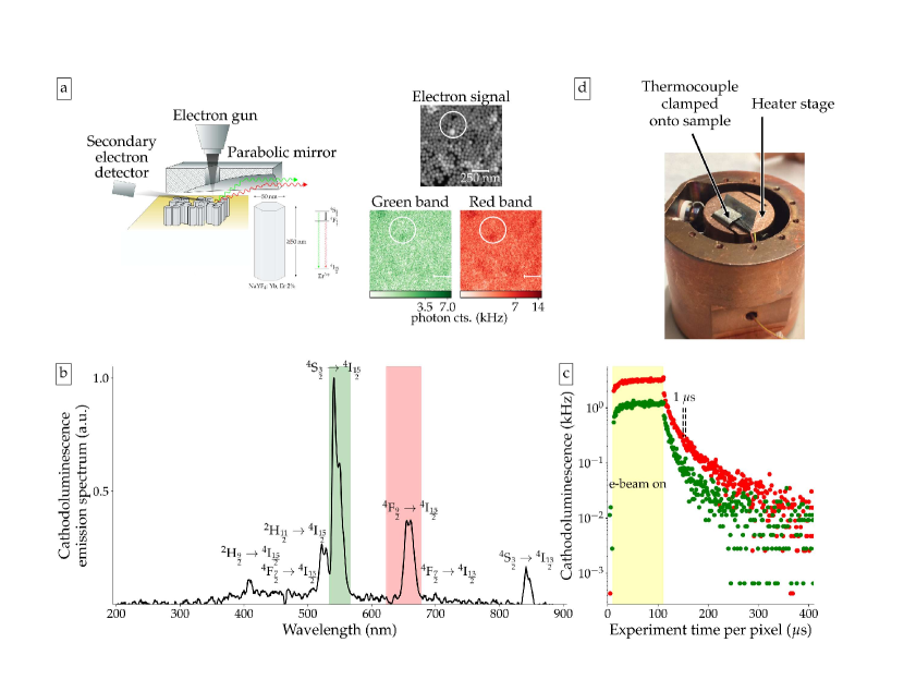
NaYF4 co-doped with Yb3+ and Er3+ has been demonstrated to be photostable up to 600 K (up to 900 K in core-shell configurations) 4 and biocompatible 5, 6, 7. As depicted in Fig. 1a, cathodoluminescence from such nanoparticles (a monolayer of hexagonal rods, nominally of 50 nm diameter, 50 nm height; drop cast on a silicon chip with a thin silicon oxide layer 200 nm) is excited by the e-beam of a field-emission scanning electron microscope (SEM). All experiments shown here were performed with an e-beam energy of 10 keV, and a current of 379 pA through a 30 m aperture.
The SEM is equipped with a custom-built parabolic mirror 24 so that the resulting cathodoluminescence is transmitted though an optical window, allowing collection of photons outside the SEM vacuum chamber. Electron and cathodoluminescence signals are acquired pixel-wise at the same time, and can be used to correlate light emission with topography, the latter obtained using the secondary electron (SE) detector.
A fast electrostatic beam blanker (rise time 25 ns) is synchronized to the scanning beam, such that pixel-wise cathodoluminescence can be recorded both under continuous excitation, and immediately after the e-beam is shut off, yielding cathodoluminescence lifetime information (minimum photon-collection integration of 40 ns, limited by the data acquisition card). The approximate instrument response function is a delta function on the ns scale (see Suppl. fig. 1c). Importantly, collection of electron and photon signals is concomitant; this means that the cathodoluminescence can be traced back to a region centered around individual nanoparticles as the secondary electron signal image is used to correlate light emission with topography.
By connecting a spectrometer to the optical port, we confirm that the cathodoluminescence emission spectrum, similarly to the fluorescence under optical excitation, is mainly due to the Er3+ ion transitions, two of which we single out for the subsequent experiments (Fig. 1b): 4S 4I and 4F 4I, respectively constituting light bands separated by 0.4 eV. The sensitivity of the spectrometer is not sufficient to acquire data from sub-m patches, and as such it is not used further in the experiments presented here, which rely exclusively on the use of more sensitive photon multiplier tubes (PMTs). Bandpass filters placed in front of the PMTs (passbands of 550 16 nm and 650 28 nm, indicated by the shaded areas in the figure) ensure that the collected cathodoluminescence is restricted to these bands. These 550 16 nm and 650 28 nm light bands are henceforth referred to as green and red wavelength bands. Given the collection efficiency of our setup, both bands produce cathodoluminescence counts in the kHz range when continuously excited. Even if the nanoparticles’ topography under cathodoluminescence is less clearly distinguishable than the electron signal, as seen in Fig. 1a, local modulations in the cathodoluminescence signal can be observed, for example, inside the white circle, which encompasses both a region devoid of nanoparticles, and one in which a NaYF4: Yb3+, Er3+ nanomaterial clump cathodoluminesces at a higher rate than the material in its vicinity.
We investigate the possibility of implementing nanoscopic thermometry using temperature-dependent changes in the cathodoluminescence of NaYF4: Yb3+, Er3+. In order to do so, we place the sample onto the open-loop, resistively-heated stage of Fig. 1d, which operates inside the SEM vacuum chamber.
In what follows, our work analyzes two features of the nanoparticles’ cathodoluminescence as a function of temperature: its mean intensity and its excited-state lifetime. We first establish a baseline of temperature sensitivity using an intensity-based method; and subsequently improve upon it by monitoring cathodoluminescence lifetime information. With the latter method, we demonstrate 30 mK temperature sensitivity in a sub-m patch.
4 Temperature information is encoded
in the cathodoluminescence intensity
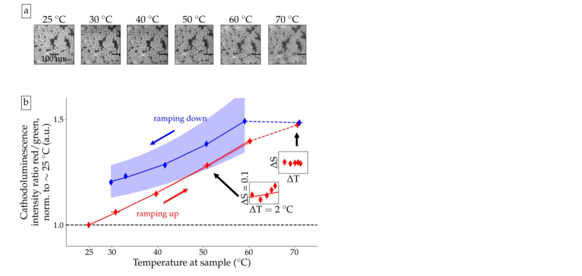
We first investigate thermal effects in the mean intensity of cathodoluminescence in the red and green light bands. Certain phonon-dependent transitions in NaYF4: Yb3+, Er3+ are known to be affected by temperature changes 3, 18, 25, 26, such that the intensity ratios of the luminescence signal of different spectral peaks can be used as a thermometer; this same effect is observed under cathodoluminescence in Fig. 2.
As measured in Suppl. fig. 5 b, even if the 4F 4I transition rate is affected by temperature changes, the 4S 4I transition has significantly larger rates at higher temperatures. The ratio of the cathodoluminescence from these two bands is stable (see Suppl. fig. 3), being independent of electron imaging parameters such as pixel size and e-beam current, and linearly depending on e-beam energy (see Suppl. fig. 4). In addition, such a ratiometric quantity does not depend on variations in nanoparticle coverage density.
The e-beam continuously excites the same nanoparticle patch (0.56 m2, with nominal nanoparticle coverage 40.2 6.8) for 150 s per 2.48 nm pixel; the mean cathodoluminescence ratio is recorded for the entire time the e-beam is un-blanked. Results over the full field-of-view are averaged, and 5 immediately consecutive frames are taken at each temperature; the total data acquisition time (not counting computer processing time) at each temperature is 12 minutes. The measured temperature at each frame is automatically recorded and averaged over to yield one data point. The temperature is ramped up and down at a rate of 10 ∘C per hour. The secondary electron signal, registered over the 5 frames, is depicted at different temperatures in Fig. 2a; re-focusing and re-centering of the SE image was performed at every temperature step; we attribute the increasing blurriness at higher temperatures to thermally-induced mechanical drifts of the sample on the heater stage. The shown micrographs are slightly different in size because we choose to analyze only the regions that are common to all 5 frames at a given temperature.
We expect the ratio of red to green cathodoluminescence to increase for increasing temperatures (a similar, spectrally-resolved result at a lower magnification is found in Suppl. fig. 5); this is due to the fact that the red 4F 4I Er+3 transition is more strongly phonon-coupled than the green 4S 4I 3.
The cathodoluminescence intensity ratio is plotted in Fig. 2b as a function of the temperature (temperature uncertainties at one standard deviation are plotted by horizontal error bars), after being normalized by the initial ratio at 25 ∘C. This normalization reduces the effects of inevitably differing PMT alignments from day to day, and of differing PMT gains at the two considered wavelength bands. When increasing the sample temperature from room-temperature, the cathodoluminescence ratio increases parabolically (higher F-statistic than a linear model). Ramping the temperature back down leads also to a parabolic (same F-statistic metric) decrease of the cathodoluminescence ratio. A hysteresis emerges, also evident in the ratio values measured at the turning point at 70 ∘C.
The insets for individual frame averages at 50 and 70 ∘C reveal that the cathodoluminescence intensity ratio () varies more steeply for a 2 ∘C temperature change at the lower temperature. We fit parabolas ( ( - 25 ∘C)2 ( - 25 ∘C) , with a fixed point 1 for the ramping up data set at increasing temperatures) to the cathodoluminescence ratios for temperatures ramping up and down; the error in the model is shown in the shaded areas (see Supplementary information for definition of error in the model).
This constitutes the first sub-m quantitative demonstration of thermal features in the cathodoluminescence intensity of lanthanide-doped nanoparticles. The limitation of using cathodoluminescence intensity ratios to perform thermometry experiments is the nanoparticles’ continuous exposure to the e-beam, which affects their mean emission in ways that could not be systematized and predicted by our experiments. Moreover, light collection efficiency fluctuations (e.g. PMTs relative alignment from day to day) would require that a calibration curve be taken at each thermometry measurement session, further increasing the nanothermometers’ exposure to e-beam radiation. We address and overcome these concerns in the following, separate approach, which is demonstrated to be sensitive to thermal effects in the mK-range based on changes in cathodoluminescence excited-state lifetimes.
5 Temperature information,
with a sensitivity down to 30 mK,
is encoded in the cathodoluminescence lifetimes
An alternative scheme can provide advantages relative to cathodoluminescence intensity-based thermometry such as reduced electron beam exposure time and independence from alignment and collection efficiency variations if excited-state lifetimes can be shown to depend on temperature; we investigate if this hypothesis holds true under cathodoluminescence here. We demonstrate that cathodoluminescence lifetimes can be used to measure relative temperature changes down to the mK-range.
Using a lifetime decay signal to perform thermometry is attractive in that the exposure of the nanothermometer to the damaging e-beam radiation is minimized. The nanoparticle needs only be excited long enough to stabilize the cathodoluminescence intensity, following a rising transient measured to be 30 s, see Suppl. fig. 3d; this shorter excitation duration translates into a five-fold decrease in radiation dose as compared to the cathodoluminescence intensity-based thermal experiments of Fig. 2. Moreover, such a (normalized) lifetime decay signal is independent of cathodoluminescence collection efficiency fluctuations and background level, which vary from day to day; of the local concentration of nanothermometers; and, importantly, on local particle damage owing to prolonged e-beam irradiation (assuming that damage is stochastic; and that only undamaged nanoparticle material contributes to the cathodoluminescence signal). Furthermore, and in contrast to intensity-based thermometry, in principle only one spectral line needs to be measured.
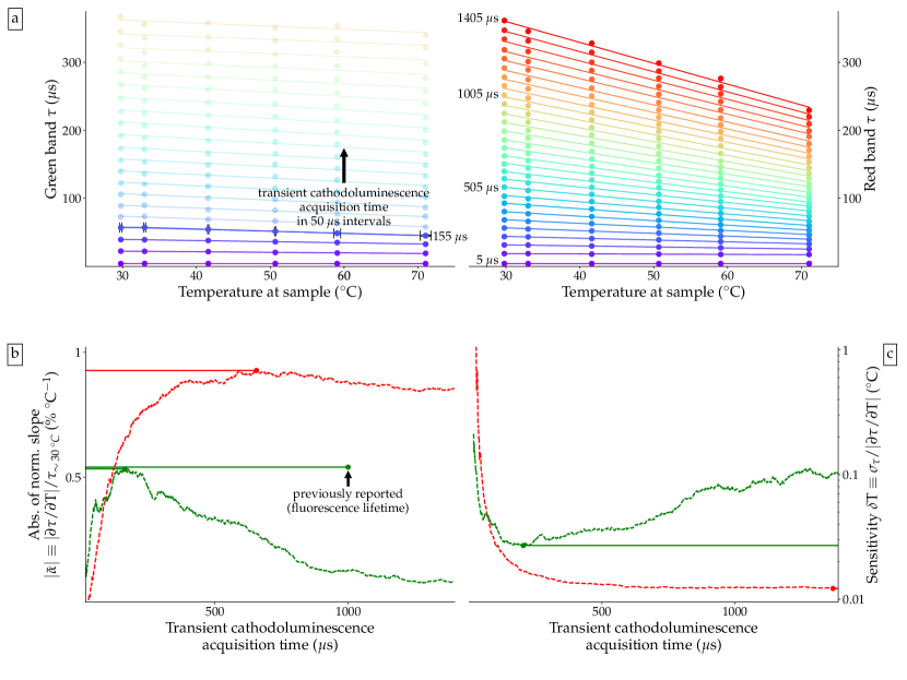
The present measurement scheme analyses the cathodoluminescence decay, pixel-by-pixel, of a nanoparticle patch (0.55 m2, with nominal nanoparticle coverage 51.2 4.8) at different temperatures, with 1 s time resolution over 1400 s following fast e-beam blanking ( 25 ns); excitation conditions are identical to the cathodoluminescence intensity ratio measurements of Fig. 2. The temperatures at the thermocouple in each frame are automatically recorded and averaged to yield a single value to represent each condition. The mean temperatures thus obtained are ∘C, in the order at which the data were taken; temperature uncertainties are indicated by black horizontal error bars signaling one standard deviation on the topmost curve of the left plot in Fig. 3a.
We define a monotonically increasing characteristic lifetime decay 7
| (1) |
where is the cathodoluminescence decay intensity in either the red or the green light band, and is the time after beam blanking (). Making use of cumulative photon counts by treating the cathodoluminescence decay intensity as a probability distribution is equivalent to low-pass filtering, and is of importance as the signal-to-noise is progressively reduced upon the measurement of an exponentially decaying quantity.
In Fig. 3a, we plot typical for the green and red bands, as a function of nanoparticle temperature, for select transient cathodoluminescence acquisition times ; different marker colors signal different , in 50 s intervals, starting at 5 s (i.e., are calculated at different temperatures, and plotted for 5, 55, 105, 155, … s following a rainbow palette). A linear fit () at each interval is shown.
The lifetimes of the normalized 4S 4I green band transition are linearly fit with slopes that approach zero. In turn, the normalized cathodoluminescence decay of the 4F 4I red band transition accelerates with increasing temperature, as expected by a phonon-assisted increase in net de-excitation probability, in an approximately linear fashion for the measured range (also observed elsewhere 7); this is apparent in the increasing slope of the linear fit at different , shown up to 1405 s. Previous optical studies have indeed found that decay lifetimes are longer for the red band transition 20.
In Fig. 3b, the absolute value of the linear best-fit slope , normalized by the characteristic lifetime taken at the lowest nanoparticle temperature of 30 ∘C 7,
| (2) |
is shown as a percentage per ∘C, for increasing times after beam blanking. In other words, quantifies the change in the apparent lifetime that we measured over a 40 ∘C range. The maximum values for each light band are indicated by a circle (at 656 and 163 s for the red and green bands, respectively, corresponding to 0.93 and 0.53 ∘C-1); also depicted is a previously reported 0.54 ∘C-1 for fluorescence lifetimes in the green band, estimated following the same method after 1000 s of transient acquisition 7.
From this plot, it is immediately clear that cathodoluminescence lifetime thermometry is more sensitive for strongly phonon-coupled transitions: analysis of the red band cathodoluminescence decay yields larger . Additionally, in the present experiments, raw cathodoluminescence counts (with e-beam on) in the red light band are 2–3.5 fold stronger than those in the green band; the exact figure depends on PMT sensitivity and alignment. Hence, the fact that sharply decreases for the green band after only 163 s is both a consequence of less strong phonon coupling controlling the dynamics of the 4S 4I transition; and of a decreased signal-to-noise ratio. The information in this plot, moreover, can be used to determine the optimal transient acquisition time, in order to achieve the most sensitive measurement.
To determine the transient acquisition time that enables the most sensitive cathodoluminescence-based temperature measurement, we numerically calculate and plot in Fig. 3c the measurement sensitivity in ∘C, or noise-limited temperature resolution, defined as 27, 28
| (3) |
Here, is the standard deviation (uncertainty) of the fitted value for , and is the unnormalized absolute value of the slope of the linear fit, or (details on the calculation of are provided in the Supplementary Information). Importantly, quantifies the magnitude of noise-related variations in the thermometry signal compared to the magnitude of changes in the parameter being measured. Effectively, represents the minimal difference in temperature that can be measured, given the available data, as a function of acquisition time. It is insensitive to the standard deviations of the measured sample temperature during calibration, even if these are substantially larger (horizontal errorbars in Fig. 3a): the measurement of the sample temperature via a thermocouple provides a calibration, and as such need not be more sensitive than the temperature information yielded by cathodoluminescence-based lifetime thermometry. Moreover, does not inform how good the nanothermometer is in measuring absolute temperatures; rather, it points to the minimum difference in temperature that would be detected by our scheme, given the noise levels. In other words, it is a measurement of precision, not accuracy. In many applications, it is indeed more relevant to measure temperature differences (eg., by how much a cancerous cell’s temperature changes as a result of exothermic anaerobic processes 29, 30) from a baseline than to measure absolute temperatures.
The optimal transient acquisition time for our cathodoluminescence-based lifetime thermometry is precisely the time that minimizes the sensitivity. In the present measurements, this optimal time is as short as 204 s for the green light band, yielding 27 mK; accordingly, in Fig. 3a, the calculated green band times are plotted in 50 s intervals up to times shorter than 204 s ( curves for longer acquisition times have essentially the same slope, confirming their low thermometry information content; they are plotted with transparency). The acquisition time that minimizes the sensitivity matches within tens of s the time for which is at a maximum. Conversely, the optimal transient acquisition time is 1370 s for the red light band, at which point sensitivity is at a minimum over the available data acquisition duration, for 12 mK. This mK-level sensitivity reflects the fact that each point in Fig. 3a is an average over 4.5 105 individual cathodoluminescence decay measurements. (A plot similar to Fig. 3, for data taken at increasing temperatures, can be found in Suppl. fig. 6; best sensitivities are on the same order of magnitude.)
6 Spatial resolution
of cathodoluminescence-based thermometry
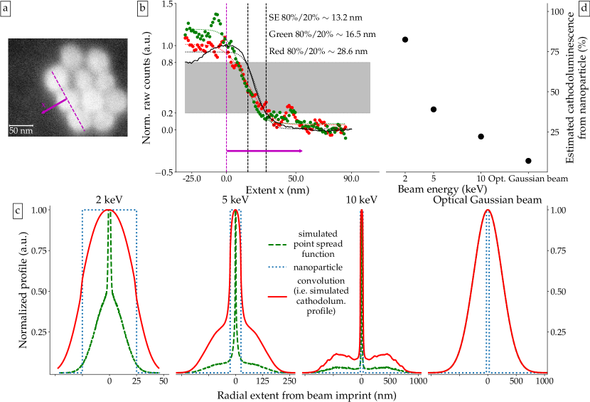
We quantify the spatial resolution of the cathodoluminescence intensity signal by comparing a feature’s edge sharpness in cathodoluminescence intensity and in the SE signal using a 10 keV e-beam. This is depicted in Fig. 4a: the dashed magenta line runs across the center of 3 nanoparticles; we quantify the steady-state luminescence and SE signal profiles along the perpendicular direction marked by the magenta arrow. Such profiles, depicted in Fig. 4b, are obtained following a 150 s-long excitation per 1.1 nm pixel, with the cathodoluminescence counts integrated over the complete excitation duration, for 10 frame averages; note that the micrograph and corresponding cathodoluminescence are acquired in less than 2 minutes. Raw photon counts and SE greyscale counts are normalized to 1 at the dashed magenta line; we estimate the edge resolution of the SE signal by the decay extent between 80 and 20 bands, obtaining 13.2 nm. We apply a 5-pixel ( 5.5 nm) moving average to the cathodoluminescence signals, and similarly estimate the decay extent to be 16.5 nm and 28.6 nm for the green and red light bands, respectively. In addition, we fit the curves to an error function (dotted lines), yielding standard deviations for the associated Gaussian of 7.4 0.2 nm, 9.9 0.4 nm, 13.0 0.9 nm for the SE, green and red curves, respectively; the values obtained by doubling these standard deviations are in good agreement with the 80 and 20 bands estimates. Both the fitted and the 80 and 20 width estimates indicate that the cathodoluminescence edge sharpness is on the same order of magnitude as the SE signal’s.
A relevant issue in the above-described thermometry scheme is quantifying how much of the cathodoluminescence signal is generated by exciting nanoparticles that are not colocalized with the primary impinging point of the electron beam, which can occur due to electron scattering inside the substrate material beneath the nanoparticles. This phenomenon, akin to the proximity effect thoroughly studied in the context of electron beam lithography 31, 32, 33, accounts for large-distance excitation of cathodoluminescence by scattered electrons, a diffuse background that degrades the intrinsic spatial resolution of cathodoluminescence-based thermometry.
We performed numerical Monte-Carlo simulations of inelastically scattered electron trajectories at different beam energies (details can be found in Suppl. fig. 7), yielding the simulated cathodoluminescence point spread functions plotted in dashed green in Fig. 4c. For 2, 5 and 10 keV beam energies, the point spread function is bi-modal; it is composed of a very tight central peak the size of the incident beam ( 2 nm), on top of a much weaker but broader diffuse background, with radii 20 nm, 150 nm and 750 nm, respectively. The simulated cathodoluminescence profile, depicted with the solid red line, is obtained after a one-dimensional convolution of the point spread function with a single nanoparticle profile, the latter depicted using the blue dotted line. Incidentally, the estimated cathodoluminescence edge sharpness of Fig. 4b are on the same order of magnitude as half-width at half-maximum of the central distribution composing the 10 keV cathodoluminescence point spread function, 33 nm.
If a uniform sheet of contiguous nanoparticles were used as nanothermometers, it is straightforward to estimate the percentage of cathodoluminescence collected from the single nanoparticle (over its 50 nm of diameter) that is directly excited by the primary electron beam aligned with its center; as compared to the undesired cathodoluminescence due to scattered electrons triggering excitations from surrounding particles. As seen in Fig. 4d, it is clear that, given the proximity effect, most luminescence intensity, even for beam energies as low as 5 keV, does not originate from the excited nanoparticle, but rather from its neighbors. At the 10 keV e-beam energy employed in our work, only 22 of the luminescence comes from the nanoparticle on which the impinging e-beam is focused. A cathodoluminescence-based thermometry signal would thus yield averaged spatial information over distances comparable to the width of the broader distribution of the point spread function (the cathodoluminescence intensity is weight-averaged by the convolutions depicted in Fig. 4c), amounting to 750 nm for the e-beam energy of 10 keV used throughout the experiments. For an e-beam energy on the order of 2 keV, however, this resolution should approach the nanoparticles’ size at 50 nm, and more than 80 of the cathodoluminescence would indeed come from the single excited particle. We provide in the Supp. fig. 7 a simulation of cathodoluminescence profiles for nearby nanoparticles excited by different e-beam energies.
For the present experiments, limitations of photon collection efficiency and electron beam current tunability prevented useful signals for beam energies lower than 10 keV from being acquired. Yet, despite the compromise in spatial resolution of nanoscale thermometry in this study at 10 keV, and which could be eliminated through further technical improvements, the present method surpasses the resolution of more typical optical methods. As shown in Fig. 4c, a Gaussian beam with a diffraction-limited waist taken to be 250 nm (full-width at half-maximum 589 nm) is simulated to excite a single nanoparticle, yielding a similarly broad luminescence profile; as estimated in Fig. 4d, if a sheet of nanoparticles were to be excited by such a Gaussian beam, less than 7 of the luminescence would come from the particle at which the excitation is centered – thus, the figure for the demonstrated cathodoluminescence method, at 22, is already more than three-fold superior. Increasing photon collection efficiency can at once improve the sensitivity (higher signal-to-noise ratios decrease ) and the resolution (enabling the use of much lower e-beam energies) of cathodoluminescence-based thermometry.
For nanoscopic thermometry, we envision using a sheet of lanthanide-doped nanoparticles drop cast onto the sample of interest. If single or sparsely-distributed nanoparticles were used as nanothermometers, the spatial resolution of the method would automatically improve, as scattered electrons would not excite nearby phosphors nor contribute to a diffuse background. In this case, only the central peak of the calculated point spread functions is relevant, and the spatial resolution is exclusively limited by the nanometric diameter of the primary e-beam. There is consequently a trade-off between temperature information coverage and spatial resolution.
An alternative scheme would have a thin film of NaYF4: Yb3+, Er3+ covering the sample of interest; the sample can be deposited or dropcast onto the thin film side which is not directly irradiated by the e-beam. The nanomaterial could be probed by the e-beam and convey temperature information, while the sample itself needs never be directly exposed to the e-beam radiation, much as in cathodoluminescence-activated imaging by resonant energy transfer (CLAIRE) 16, 17. In CLAIRE as in our proposed thermometry scheme, low e-beam energies are required to ensure that most e-beam radiation is fully absorbed before reaching the sample (see see Suppl. fig. 7). This format would be compatible with the electron microscope vacuum chamber; as would biological samples placed in electron microscope-compatible liquid cells 34, 35, 36.
7 Conclusion
In conclusion, we have demonstrated a nanoscopic thermometry scheme based on the cathodoluminescence of NaYF4: Yb3+, Er3+ nanoparticles, shown to be temperature-dependent at the sub-m level. The mean cathodoluminescence ratio of two Er3+ transitions could not, in our available data, be shown to yield reproducible changes contingent on the temperature of a sub-m nanoparticle patch, presumably due to damage caused by prolonged e-beam irradiation. The lifetimes of such transitions, after fast e-beam blanking, were shown to depend on temperature in a linear fashion, yielding a measurement sensitivity on the order of 30 mK. The key advantage of cathodoluminescence-based lifetime thermometry stems from the fact that excited-state lifetimes are independent of variations in cathodoluminescence collection efficiency and background level, and of e-beam damage (all of which only alter signal-to-noise levels). In addition, and in contrast to intensity-based thermometry, there is no need to correlate multiple spectral lines. At the used e-beam energy of 10 keV, the cathodoluminescence edge spatial resolution is comparable to the electron signal’s, even though the photon signal does not only stem from the directly excited region, but from a broader area 750 nm in radius; this figure is limited by cathodoluminescence excitation away from the e-beam scanning point due to electron scattering but is still superior to the resolution of excitation by a diffraction-limited optical Gaussian beam. It can moreover be improved by using lower-energy e-beams (for example, enabled by a higher-efficiency photon collection apparatus); it was calculated that a 2 keV e-beam would yield a resolution compared to the nanoparticles’ size. We envision the implementation of cathodoluminescence-based thermometry with NaYF4: Yb3+, Er3+ in two ways. First, using a single nanoparticle as a thermometer (on top of a sample that can withstand e-beam irradiation, such as miniaturized electronics) can immediately provide nanometric spatial resolution with the method described here. Second, a sheet of nanoparticles covering a sample, or a NaYF4: Yb3+, Er3+ thin film under which a sample is deposited (or that is fabricated over a sample), can also function as a barrier against direct e-beam irradiation, thereby providing a platform for temperature diagnostics of delicate and biological specimens. The experiments reported here thus represent the first steps towards non-contact cathodoluminescence-based thermometry at the nanoscale.
8 Sample preparation
A sample of commercial NaYF4: Yb3+, Er3+ (Mesolight Inc.) was drop cast on top of a silicon chip with 200 nm of silicon dioxide (deposited by plasma-enhanced chemical vapor). It was left to dry under ambient conditions.
Before the first electron microscopy session, the sample was gently cleaned for 2 minutes in an oxygen plasma in order to remove putative chemical residuals causing spurious cathodoluminescence emission (see Suppl. fig. 1). The same sample is used in all experimental runs, being subject to many thermal cycles.
9 Cathodoluminescence measurements
A Zeiss Gemini Supra 55 SEM is retrofit with a home-built parabolic mirror 24 in order to enable cathodoluminescence measurements. Custom software (ScopeFoundry 37, 38) synchronizes and controls a Raith 50 electrostatic beam blanker that can nominally pulse the e-beam with duty cycles as short as 1 s; measured rise times are 25 ns.
The specimen’s temperature was changed using a home-built, open-loop heater stage placed inside the electron microscope’s vacuum chamber. A metal clip pressed the chip containing the sample onto a copper surface; a K-type thermocouple was spot-welded to the inside of the metal clip, and as such was in contact with the sample side of the chip at all times. Thermal carbon paste was placed on the silicon chip, whose surface was in contact with the copper. Voltage readings from the thermocouple were amplified and automatically collected with the same frequency as the voltage readings yielded by the secondary electron detector. Voltage readings from the thermocouple were treated in the same fashion as the cathodoluminescence photon signal (eg., frame averaging) before conversion to temperature.
A Hamamatsu R6094 (Hamamatsu H7421) PMT is used to record photons within the green (red) wavelength band. Bandpass filters are placed in the optical path before the PMTs (550/32 nm Semrock Brightline FF01-550/32-25 and 650/54 nm Semrock Brightline FF01-650/54-25). Absolute cathodoluminescence intensities vary on a daily basis given the apparatus’ optical alignment and sensitivity.
Both analog signals from the SEM’s secondary electron detector, and digital signals from the PMTs are recorded by a National Instruments PXIe-6363 card.
Spectrally resolved cathodoluminescence measurements have been taken using a Ocean Optics QE65 spectrometer.
10 Acknowledgments
This work was supported by the Chemical Sciences, Geosciences and Biosciences Division, Office of Basic Energy Sciences, Office of Science, U.S. Department of Energy, FWP number SISGRN. Cathodoluminescence measurements at the Lawrence Berkeley National Laboratory Molecular Foundry were performed as part of the Molecular Foundry user program, supported by the Office of Science, Office of Basic Energy Sciences, of the U.S. Department of Energy under Contract No. DE-AC02-05CH11231. The preparation of this manuscript was supported by STROBE, a National Science Foundation Science Technology Center under Grant No. DMR 1548924. C. D. Aiello acknowledges insightful discussions with Ayelet Teitelboim and Boerge Hemmerling, and assistance with the heater stage from Connor Bischak. A. D. Pickel and R. B. Wai acknowledge NSF Graduate Research Fellowships (DGE 1106400). N. S. Ginsberg acknowledges an Alfred P. Sloan Research Fellowship, a David and Lucile Packard Foundation Fellowship for Science and Engineering, and a Camille and Henry Dreyfus Teacher-Scholar Award.
References
- Menges et al. 2016 Menges, F.; Mensch, P.; Schmid, H.; Riel, H.; Stemmer, A.; Gotsmann, B. Nat. Comms. 2016, 7, 10874
- Haase and Schaefer 2011 Haase, M.; Schaefer, H. Angew. Chem. Int. Ed. 2011, 50, 5808
- Chan et al. 2012 Chan, E. M.; Han, G.; Goldberg, J. D.; Gargas, D. J.; Ostrowski, A. D.; Schuck, P. J.; Cohen, B. E.; Milliron, D. J. Nano Lett. 2012, 12, 3839
- Geitenbeek et al. 2017 Geitenbeek, R. G.; Prins, P. T.; Albrecht, W.; van Blaaderen, A.; Weckhuysen, B. M.; Meijerink, A. J. Phys. Chem. C 2017, 121, 3503
- Li et al. 2015 Li, Z.; Lv, S.; Wang, Y.; Chen, S.; Liu, Z. J. Am. Chem. Soc. 2015, 137, 3421
- Dai et al. 2013 Dai, Y.; Xiao, H.; Liu, J.; Yuan, Q.; Ma, P.; Yang, D.; Li, C.; Cheng, Z.; Hou, Z.; Yang, P.; Lin, J. J. Am. Chem. Soc. 2013, 135, 18920
- Savchuk et al. 2014 Savchuk, O. A.; Haro-Gonzalez, P.; Carvajal, J. J.; Jaque, D.; Massons, J.; Aguilo, M.; Diaz, F. Nanoscale 2014, 6, 9727
- Du et al. 2017 Du, P.; Luo, L.; Yu, J. S. Appl. Phys. A. 2017, 123, 157
- Yu et al. 2014 Yu, W.; Xu, W.; Song, H.; Zhang, S. Dalton Trans. 2014, 43, 6139
- Rohani et al. 2015 Rohani, S.; Quintanilla, M.; Tuccio, S.; de Angelis, F.; Cantelar, E.; Govorov, A. O.; Razzari, L.; Vetrone, F. Adv. Optical Mater 2015, 3, 1606
- Catalano et al. 2017 Catalano, M. R.; Pellegrino, A. L.; Rossi, P.; Paoli, P.; Cortelletti, P.; Pedroni, M.; Speghini, A.; Malandrino, G. New J. Chem. 2017, 41, 4771
- Betzig 2015 Betzig, E. Rev. Mod. Phys. 2015, 87, 1153
- Schermelleh et al. 2010 Schermelleh, L.; Heintzmann, R.; Leonhardt, H. J. Cell Biol. 2010, 190, 165
- Betzig et al. 1986 Betzig, E.; Lewis, A.; Harootunian, A.; Isaacson, M.; Kratschmer, E. Biophys. J. 1986, 49, 269
- Harootunian et al. 1986 Harootunian, A.; Betzig, E.; Isaacson, M.; Lewis, A. Appl. Phys. Lett. 1986, 49, 674
- Bischak et al. 2015 Bischak, C. G.; Hetherington, C. L.; Wang, Z.; Precht, J. T.; Kaz, D. M.; Schlom, D. G.; Ginsberg, N. S. Nano Lett. 2015, 15, 3383
- Bischak et al. 2017 Bischak, C. G.; Wai, R. B.; Cherqui, C.; Busche, J. A.; Quillin, S. C.; Hetherington, C. L.; Wang, Z.; Aiello, C.; Schlom, D. G.; Aloni, S.; Ogletree, D. F.; Masiello, D. J.; Ginsberg, N. S. ACS Nano 2017, 11, 10583
- Yu et al. 2016 Yu, D.; Ballato, J.; Riman, R. E. J. Phys. Chem. C 2016, 120, 9958
- Wisser et al. 2016 Wisser, M. D.; Fischer, S.; Maurer, P. C.; Bronstein, N. D.; Chu, S.; Alivisatos, A. P.; Salleo, A.; Dionne, J. A. ACS Photonics 2016, 3, 1523
- Hyppaenen et al. 2017 Hyppaenen, I.; Hoeysniemi, N.; Arppe, R.; Schaeferling, M.; Soukka, T. J. Phys. Chem. C 2017, 121, 6924
- Cho et al. 2017 Cho, Y.; Song, S. W.; Lim, S. Y.; Kim, J. H.; Park, C. R.; Kim, H. M. Phys. Chem. Chem. Phys. 2017, 19, 7326
- de Abajo 2010 de Abajo, F. J. G. Rev. Mod. Phys. 2010, 82, 209
- Sinha et al. 2017 Sinha, S.; Mahata, M. K.; Swart, H. C.; Kumar, A.; Kumar, K. New J. Chem. 2017, 41, 5362
- Kaz et al. 2013 Kaz, D. M.; Bischak, C. G.; Hetherington, C. L.; Howard, H. H.; Marti, X.; Clarkson, J. D.; Adamo, C.; Schlom, D. G.; Ramamoorthy, R.; Aloni, S.; Ogletree, D. F.; Ginsberg, N. S. ACS Nano 2013, 7, 10397
- Fischer et al. 2011 Fischer, L. H.; Harms, G. S.; Wolfbeis, O. S. Angew. Chem. Int. Ed. 2011, 50, 4546
- Sedlmeier et al. 2012 Sedlmeier, A.; Achatz, D. E.; Fischer, L. H.; Gorris, H. H.; Wolfbeis, O. S. Nanoscale 2012, 4, 7090
- Groeger et al. 2006 Groeger, S.; Bison, G.; Schenker, J. L.; Wynands, R.; Weis, A. Eur. Phys. J. D 2006, 38, 239
- Balabhadra et al. 2017 Balabhadra, S.; Debasu, M. L.; Brites, C. D. S.; Ferreira, R. A. S.; Carlos, L. D. J. Phys. Chem. C 2017, 121, 13962
- Gogvadze et al. 2008 Gogvadze, V.; Orrenius, S.; Zhivotovsky, B. Trends Cell Biol. 2008, 18, 165
- MG et al. 2009 MG, M. G. V. V. H.; Cantley, L. C.; Thompson, C. B. Science 2009, 324, 165
- Ren and Chen 2004 Ren, L.; Chen, B. Proceedings of the 7 International Conference on Solid-State and Integrated Circuits Technology 2004, 1, 579
- Owen 1990 Owen, G. J. Vac. Sci. Technol. B 1990, 8, 1889
- Chang 1975 Chang, T. H. P. J. Vac. Sci. Technol. 1975, 12, 1271
- Yuk et al. 2012 Yuk, J. M.; Park, J.; Ercius, P.; Kim, K.; Hellebusch, D. J.; Crommie, M. F.; Lee, J. Y.; Zettl, A.; Alivisatos, A. P. Science 2012, 6, 336
- Park et al. 2015 Park, J.; Park, H.; Ercius, P.; Pegoraro, A. F.; Xu, C.; Kim, J. W.; Han, S. H.; Weitz, D. A. Nano Lett. 2015, 15, 4737
- Wojcik et al. 2015 Wojcik, M.; Hauser, M.; Li, W.; Moon, S.; Xu, K. Nat. Comms. 2015, 6, 7384
- 37 http://www.scopefoundry.org
- Durham et al. 2018 Durham, D. B.; Ogletree, D. F.; Barnard, E. S. Surf. Interface Anal. 2018, ECASIA special issue paper