Chip-integrated voltage sources for control of trapped ions
Abstract
Trapped-ion quantum information processors offer many advantages for achieving high-fidelity operations on a large number of qubits, but current experiments require bulky external equipment for classical and quantum control of many ions. We demonstrate the cryogenic operation of an ion-trap that incorporates monolithically-integrated high-voltage CMOS electronics ( full swing) to generate surface-electrode control potentials without the need for external, analog voltage sources. A serial bus programs an array of 16 digital-to-analog converters (DACs) within a single chip that apply voltages to segmented electrodes on the chip to control ion motion. Additionally, we present the incorporation of an integrated circuit that uses an analog switch to reduce voltage noise on trap electrodes due to the integrated amplifiers by over . We verify the function of our integrated electronics by performing diagnostics with trapped ions and find noise and speed performance similar to those we observe using external control elements.
I Introduction
Quantum computers and simulators based on trapped atomic ions have great potential to allow for the execution of complex algorithms, but to date, experiments have been limited to tens of ion qubits. Increasing the size of linear chains of ions presents experimental challenges including optical addressing and control of individual ions, arbitrary re-ordering of ion positions during complex protocols, and limited lifetimes of long chains Kaufmann et al. (2017); Pagano et al. (2018). Alternatively, array-based designs which naturally solve these issues have been discussed recently Kielpinski et al. (2002); Lekitsch et al. (2017). The array architecture has a clearer path toward increasingly-complex designs and might also benefit from modern semiconductor fabrication techniques. These architectures will require integration of control elements into the vacuum chamber to reduce the number of required interconnects. Off-the-shelf electronics have been modified and attached to trap hardware in-vacuum Eltony et al. (2013); Guise et al. (2014), but as array architectures expand beyond tens of control zones, the required circuitry for electrode control within a zone will occupy significantly more area than the footprint of an array site. Integrating devices into the trap array itself could potentially solve this scaling problem, but this design will require a tradeoff among device area, power, speed, and noise. Beyond quantum information processing, other chip-based technologies, like miniature atomic clocks Delehaye and Lacroûte (2018) or sensors Salim et al. (2011) could also benefit from these highly-integrated, low-power control systems.
In this work, we advance the integration of control voltages to the microscopic level by presenting a design for a voltage source, with performance similar to modern external sources, that is incorporated into the substrate beneath the electrodes of an ion trap. Surface electrode ion traps are typically fabricated in custom lithographic processes that involve deposition and patterning of a few metal layers Seidelin et al. (2006); Stick et al. (2006); Amini et al. (2010); Hughes et al. (2011); Mielenz et al. (2016); Bruzewicz et al. (2016). Recently, it has been shown that planar ion traps can also be manufactured in commercial CMOS processes, which offer improved design reproducibility and can reduce fabrication costs of more complex devices Mehta et al. (2014). Here we extend the foundry-produced ion trap design to include voltage sources integrated into the semiconductor substrate. Adding active electronics in such close proximity to the trap presents a challenge since ions are sensitive to both the static and fluctuating electric fields generated within the integrated circuit. We carefully characterize the noise and speed of these chip-integrated devices for quantum information applications; the architecture may also be of general interest in deployable systems, due to the high repeatability and functionality afforded by CMOS technology. Explorations such as this, which evaluate the performance of quantum systems with advanced classical control, are key to assessing the utility of modern control technology for future quantum sensors, simulators, and computers.
II High-Voltage Digital-to-Analog Converter Design
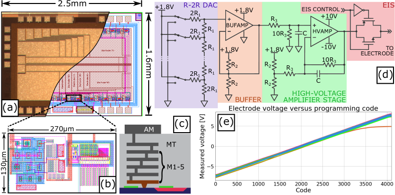
Voltages are derived from an R-2R resistor ladder digital-to-analog converter (DAC) Horowitz and Hill (2015) with 12-bits of resolution and an output range of approximately (see Fig. 1). The DAC accepts a 12-bit code word that it translates to an analog voltage on its output (see example data in Fig. 1e). We program the DACs using an integrated serial peripheral interface (SPI) bus, controlled by an external field-programmable gate array (FPGA) running custom firmware. The ion trap has 16 control electrodes, with one DAC to independently bias each one. Data is serially daisy chained through the SPI bus, for a total of bits of voltage data. In order to update the voltage on any or all electrodes, the full 192-bit string is sent to the chip.
The devices were fabricated as part of a multi-project wafer through MOSIS in the Global Foundries CMHV7SF node. We chose this process for its compatibility with high voltages (up to ) which are necessary to achieve ion trapping frequencies around for in typical ion traps. The process includes 7 metal layers (Fig. 1c); the topmost metal layer (AM), consisting of -thick aluminum, is used to define the trap electrode geometry, which is designed to trap ions at a height of . The next lower layer (MT) forms a ground plane to isolate the ion from digital and power supply noise in the internal layers of the DAC, to isolate the DAC from pickup due to the large RF voltage on the top of the chip, and to shield the ion from laser-induced effects of carrier generation in the silicon substrate Mehta et al. (2014). The remaining metal layers route digital and analog signals between the CMOS transistors defined in the silicon substrate and the serial inputs and control electrodes on the top metal. Since each high-voltage transistor is comparatively large (, about of the total DAC block area in Fig. 1b), we try to use as few as possible. Hence, the first two stages of the circuit, depicted in Fig. 1d, are formed using only smaller, low-voltage CMOS devices. The number of transistors in the high-voltage amplifier (HVAMP) is also minimized, which reduces input impedance and limits the output range to instead of the full-scale set by the power supplies. Due to the low input impedance, a low-voltage buffer amplifier (BUFAMP) was added between the R-2R DAC and the high-voltage amplifier stage so that current in the DAC does not leak into the HVAMP.
III DAC Characterization
In our apparatus, we cool the ion trap to cryogenic temperatures (), since this has been shown to reduce electric field noise from the trap surface and also removes the need to bake the vacuum chamber for several days to reach ultra-high vacuum Labaziewicz et al. (2008); Bruzewicz et al. (2015). Cryogenic operation comes with challenges in the integrated circuit performance, since the specifications provided by the CMOS foundry do not characterize behavior at temperatures below . Thus we sacrifice some of the reproducibility usually afforded by CMOS and must ensure basic operation at our chosen temperature. We first test the DACs on the bench by connecting the trap chip to an interposing circuit board. The test assembly is immersed in liquid nitrogen or helium while we perform a sweep of programming codes and measure the resultant voltage on the output. We find that some DAC channels lose the requisite linearity between programming code and output voltage as they cool to cryogenic temperature, as in Fig. 1e. For this reason, we add wire bonds to the edge of each electrode so that DAC voltages may be monitored and calibrated while conducting experiments with ions. In future designs, we plan to add an internal multiplexer for routing the voltages to a single diagnostic pad, obviating the need for the extra bonds.
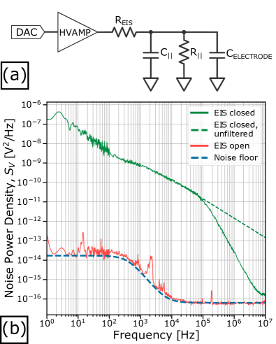
We can correct for DC voltage error in the DAC output by simply adding an offset to the programmed value. Noise at the output of the high-voltage amplifier, which cannot be calibrated away, presents a more fundamental concern for quantum logic gates based on shared motional states of chains of ions Häffner et al. (2008). We characterize the noise of the integrated voltage source in an external test fixture (Fig. 2b, green trace). The extrapolated, unfiltered noise at (dashed green trace), , is a few orders of magnitude above state-of-the-art integrated circuits with similar update speed, which have voltage noise as low as –, though in a larger footprint 111See for instance the Analog Devices AD5790 or the Texas Instruments TI-DAC8881.. Noise on external voltage sources can be mitigated using commercial, rack-mountable low-pass filter arrays with several orders of magnitude of suppression at relevant ion frequencies. On the integrated device, filtering options are limited since we cannot define arbitrary inductors and capacitors on-chip due to the small size of the circuit. Standard passive filtering also permanently reduces the overall bandwidth of the system and places a limit on the speed of ion transport operations. To solve these problems, we have designed a switchable filter by placing a complementary pair of high-voltage field-effect transistors (FETs) between the output of the amplifier and the trap electrode, shown in the schematic of Fig. 1d. For clarity, we will refer to this device as the electrode isolation switch(es) or EIS.
The EIS approximates the function of a mechanical relay, in which no current flows and the noise voltage is perfectly attenuated when the EIS is open. More precisely, the EIS is a voltage-variable resistance which is approximately when closed and when open. On the bench, we measure a noise power attenuation of up to six orders of magnitude after opening the EIS. This measurement is limited by the noise floor of our instruments (see Fig. 2b), so the actual isolation may be much higher. Since trap electrodes behave as capacitors with very low leakage, we can quickly manipulate trap voltages with the EIS closed and then effectively disconnect the electrodes from the amplifier noise by opening the EIS, while the trapping voltages are maintained. In more complex designs, the EIS could also be used for switching between multiple integrated voltage sources, which has been shown to be useful in experiments with fast ion transport Alonso et al. (2013, 2016).
IV Operation with Trapped Ions
During experiments with ions, we operate the trap in a cryogenic vacuum apparatus (described in Bruzewicz et al. (2016)). The ion trap is thermally anchored to the cold head of a cryostat via a ceramic pin grid array (CPGA) and a custom printed circuit board. An RF signal with an amplitude of at provides ponderomotive confinement of ions in two (radial) dimensions. The DC voltages programmed by the DACs define the trapping potential along the third (axial) direction. Neutral atoms are introduced into the region above the trap by accelerating a pre-cooled cloud of atoms in a 2D MOT with a resonant “push” beam Sage et al. (2012). We trap after two-photon photoionization via excitation at and . Ions are Doppler cooled with light at to about . A repumping laser at prevents shelving in the long-lived state (see e.g. Bruzewicz et al. (2017) for an illustration of the electronic energy levels of ). A stable and narrow laser at addresses the quadrupole transition, which we use to read out the ion’s motional state and perform resolved motional-sideband cooling close to the ground state of axial motion () Leibfried et al. (2003).
After applying the relatively high-voltage RF potential to the chip, we confirm that the DACs are still operational by sweeping through all possible programming codes while monitoring the voltage on each electrode via the monitor wire bonds. We find no difference in performance, even when applying RF voltages of up to . We have programmed the DAC voltages to demonstrate trapping of calcium ions at axial frequencies from up to . We have also performed rudimentary ion transport over a distance of at by writing a continuous stream of voltages to trap electrodes at a SPI clock speed of . Ion motion is verified by watching ion fluorescence on an electron-multiplying CCD camera while the ion is repeatedly shuttled back and forth by varying the DAC voltages with the EIS closed. Ions were shuttled over hundreds of cycles without loss. When DAC voltages are fixed, trap lifetimes are similar to those we observe in standard planar traps controlled by external voltages sources ( seconds without cooling lasers, and several hours with Doppler cooling). We finely adjust the internal voltages to trim out stray electric fields, due primarily to charging from photoionization lasers Harlander et al. (2010); Wang et al. (2011), in order to eliminate excess micromotion induced by the RF potential Sedlacek et al. (2018). We verify that trap voltages do not drift when the EIS is open by monitoring the trapped ion’s position and trapping frequency and find that we can leave the EIS open for several minutes with no noticeable effect to the potential at the ion’s location.
Voltage noise on the trap electrodes heats the average motional state, , of the ion in the trap potential reducing the fidelity of quantum logic gates between ion qubits Turchette et al. (2000); Kirchmair et al. (2009). We can quantify this effect using standard techniques for measuring heating rates of trapped ions Brownnutt et al. (2015). The relationship between voltage noise power and the heating rate of the motional mode, , is given by:
| (1) |
where and are the mass and charge of the ion, is the (angular) trap frequency, is the square of the voltage noise spectral density and is a geometric factor determined by the distance from the ion to the trap and the shape of the control electrodes Leibrandt et al. (2007). We calculate the value of using a finite-element electrostatic simulation to determine the electric field at the ion’s position for a given voltage applied to the trap electrodes. From measurements of with the EIS open and closed, we can determine the voltage noise, and thus quantify the isolation of the EIS.
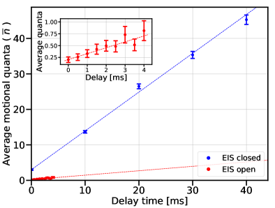
In Fig. 3, we present the average motional state of the ion as a function of delay after resolved-sideband cooling, from which we determine the heating rate. With the EIS closed, we can compare the heating rate and voltage noise, derived via Eq. (1), with the bench measurement in Fig. 2b, but we must account for additional filtering seen by the ion. The wire bonds that we use to monitor DAC voltages put the trap electrodes in parallel with extra capacitance from a filter board (). The filter capacitor alone makes a pole at when the switch is closed () and reduces the expected voltage noise from to at . This is in agreement with the voltage noise obtained from the heating rate in Fig. 3, , within a factor of two. With the EIS open, the voltage noise is below the noise floor of our spectrum analyzer (Fig. 2b), so we expect a heating rate of or lower. The measured heating rate with the EIS open, , is below this limit, but the noise is not reduced by as much as expected given the high isolation of the EIS at lower frequencies.
To further investigate the limitations to the heating rate with the EIS open, we attached a temperature-sensing diode to the surface of the chip. We found that the temperature of the chip increases from to just above when powered on in the CPGA mount. This temperature increase is due to the power dissipation of the chip-integrated DACs (), the limited cooling power of the cryostat, and the thermal resistance of the CPGA heatsink 222In an upcoming revision of the chip, we have included a power-down feature which can reduce the power consumption to after trap electrodes have charged up and the EIS is opened.. At , we expect anomalous electric field noise, arising from the surface of the electrode metal, rather than technical noise in the voltage sources, to limit the heating rate to – Brownnutt et al. (2015); Bruzewicz et al. (2015), which is in agreement with our measurement in this work.
V Output Bandwidth and Filtering
Finally, we consider the maximum update rate of the voltage sources. Serialization of input data comes with a speed tradeoff, since trap voltages may only be updated after sending 12 bits to each of the 16 DAC channels. From SPICE simulation Nagel and Pederson (1973), we determine the highest data rate of the SPI bus to be (maximum voltage update rate , due to the length of the 192-bit input string); however, in our experiment, we have achieved SPI data rates of (voltage update rate of ). Above this speed, there is a sharp decrease in the fidelity of the digital-to-analog conversion. We presume this limit comes from reflections in the data lines into the vacuum chamber, since this has previously been a source of error in our experience with this SPI bus design. Using controlled-impedance lines and terminations at the chip would help to reduce these reflections.
In practice, any voltage updates on the trap electrodes are ultimately limited by the pole at created by the “on” resistance of the EIS () and the capacitance on the filter board (). The relatively large resistance of the EIS is not fundamental, and can be reduced in subsequent design revisions. We could also improve this bandwidth by reducing the parallel filter capacitance, , but this requires careful consideration. This capacitor also attenuates the Johnson noise associated with the large () “off” resistance of the EIS; however, at relevant ion frequencies around , for parallel capacitance of even a few , this noise source is much smaller than that due to the resistance of the electrode metal and the equivalent series resistance of the capacitor. More significantly, the additional capacitance to ground shunts leakage from the RF electrode onto the control electrode surfaces by forming a capacitive voltage divider with the effective capacitance between the electrodes Doret et al. (2012). From electrostatic simulation, we find that approximately of the RF voltage, if present on the other trap electrodes, can significantly reduce the depth of the potential well seen by the ion. Acting conservatively, we might choose to keep the RF leakage below . The simulated capacitance between the RF and DC electrodes is between and , so this requires a shunting capacitance of to . With these values, we would expect the bandwidth with the EIS closed to be - and the isolation with the EIS open to be , which should suppress the DAC technical noise to the same level as the Johnson noise due to the resistance of the trap metal, far below the level of electric field noise due to anomalous heating for traps of this size Brownnutt et al. (2015). On our chip, a capacitor could be integrated in the lower metal layers for each of the trap electrodes without increasing the total device area.
VI Conclusion
We have demonstrated the operation of the first ion trap with electrode-control voltage sources embedded into the trap substrate. With the addition of the electrode isolation switch, these sources approach the noise level of standard voltage sources. The development of these DACs is an important milestone on the way to realizing more complex trapped-ion-system architectures, and our characterization of their performance will be key to assessing their potential for future quantum information processing applications.
VII Acknowledgements
We thank Hernan Castro and George Fitch for layout assistance, Peter Murphy, Chris Thoummaraj, and Lee Mailhiot for assistance with chip packaging, and Terry Weir and Gerry Holland for assistance with the bench test setup. This work was sponsored by the Assistant Secretary of Defense for Research and Engineering under Air Force contract number FA8721-05-C-0002. Opinions, interpretations, conclusions, and recommendations are those of the authors and are not necessarily endorsed by the United States Government.
References
- Kaufmann et al. (2017) H. Kaufmann, T. Ruster, C.T. Schmiegelow, M.A. Luda, V. Kaushal, J. Schulz, D. von Lindenfels, F. Schmidt-Kaler, and U.G. Poschinger, “Fast ion swapping for quantum-information processing,” Phys. Rev. A 95, 052319 (2017).
- Pagano et al. (2018) G. Pagano, P.W. Hess, H.B. Kaplan, W.L. Tan, P. Richerme, P. Becker, A. Kyprianidis, J. Zhang, E. Birckelbaw, M.R. Hernandez, Y. Wu, and C. Monroe, “Cryogenic trapped-ion system for large scale quantum simulation,” (2018), arXiv:1802.031118v1 .
- Kielpinski et al. (2002) D. Kielpinski, C. Monroe, and D.J. Wineland, “Architecture for a large-scale ion-trap quantum computer,” Nature 417, 709–711 (2002).
- Lekitsch et al. (2017) B. Lekitsch, S. Weidt, A.G. Fowler, K. Mølmer, S.J. Devitt, C. Wunderlich, and W.K. Hensinger, “Blueprint for a microwave trapped ion quantum computer,” Sci. Adv. 3, e1601540 (2017).
- Eltony et al. (2013) A.M. Eltony, S.X. Wang, G.M. Akselrod, P.F. Herskind, and I.L. Chuang, “Transparent ion trap with integrated photodetector,” Appl. Phys. Lett. 102, 054106 (2013).
- Guise et al. (2014) N.D. Guise, S.D. Fallek, H. Hayden, C.-S. Pai, C. Volin, K.R. Brown, J.T. Merrill, A.W. Harter, J.M. Amini, L.M. Lust, K. Muldoon, D. Carlson, and J. Budach, “In-vacuum active electronics for microfabricated ion traps,” Rev. Sci. Instrum 85, 063101 (2014).
- Delehaye and Lacroûte (2018) M. Delehaye and C. Lacroûte, “Single-ion, transportable optical atomic clocks,” J. Mod. Opt. 65, 622–639 (2018).
- Salim et al. (2011) E.A. Salim, J. DeNatale, D.M. Farkas, K.M. Hudek, S.E. McBride, J. Michalchuk, R. Mihailovich, and D.Z. Anderson, “Compact, microchip-based systems for practical applications of ultracold atoms,” Quantum Inf. Process. 10, 975–994 (2011).
- Seidelin et al. (2006) S. Seidelin, J. Chiaverini, R. Reichle, J.J. Bollinger, D. Leibfried, J. Britton, J.H. Wesenberg, R.B. Blakestad, R.J. Epstein, D.B. Hume, W.M. Itano, J.D. Jost, C. Langer, R. Ozeri, N. Shiga, and D.J. Wineland, “Microfabricated surface-electrode ion trap for scalable quantum information processing,” Phys. Rev. Lett. 96, 253003 (2006).
- Stick et al. (2006) D. Stick, W.K. Hensinger, S. Olmschenk, M.J. Madsen, K. Schwab, and C. Monroe, “Ion trap in a semiconductor chip,” Nat. Phys. 2, 36–39 (2006).
- Amini et al. (2010) J.M. Amini, H. Uys, J.H. Wesenberg, S. Seidelin, J. Britton, J.J. Bollinger, D. Leibfried, C. Ospelkaus, A.P. VanDevender, and D.J. Wineland, “Toward scalable ion traps for quantum information processing,” New J. Phys. 12, 033031 (2010).
- Hughes et al. (2011) M.D. Hughes, B. Lekitsch, J. Broersma, and W. Hensinger, “Microfabricated ion traps,” Contemp. Phys. 52, 505–529 (2011).
- Mielenz et al. (2016) M. Mielenz, H. Kalis, M. Wittemer, F. Hakelberg, U. Warring, R. Schmied, M. Blain, P. Maunz, D.L. Moehring, D. Leibfried, and T. Schaetz, “Arrays of individually controlled ions suitable for two-dimensional quantum simulations,” Nat. Commun. 7, 11839 (2016).
- Bruzewicz et al. (2016) C.D. Bruzewicz, R. McConnell, J. Chiaverini, and J.M. Sage, “Scalable loading of a two-dimensional trapped-ion array,” Nat. Commun. 7, 13005 (2016).
- Mehta et al. (2014) K.K. Mehta, A.M. Eltony, C.D. Bruzewicz, I.L. Chuang, R.J. Ram, J.M. Sage, and J. Chiaverini, “Ion traps fabricated in a CMOS foundry,” Appl. Phys. Lett. 105, 044103 (2014).
- Horowitz and Hill (2015) Paul Horowitz and Winfield Hill, The Art of Electronics, 3rd ed. (Cambridge University Press, 2015).
- Labaziewicz et al. (2008) J. Labaziewicz, Y. Ge, D.R. Leibrandt, S.X. Wang, R. Shewmon, and I.L. Chuang, “Temperature dependence of electric field noise above gold surfaces,” Phys. Rev. Lett. 101, 180602 (2008).
- Bruzewicz et al. (2015) C.D. Bruzewicz, J.M. Sage, and J. Chiaverini, “Measurement of ion motional heating rates over a range of trap frequencies and temperatures,” Phys. Rev. A 91, 041402 (2015).
- Häffner et al. (2008) H. Häffner, C.F. Roos, and R. Blatt, “Quantum computing with trapped ions,” Phys. Rep. 469, 155 – 203 (2008).
- Note (1) See for instance the Analog Devices AD5790 or the Texas Instruments TI-DAC8881.
- Alonso et al. (2013) J. Alonso, F.M. Leupold, B.C. Keitch, and J.P. Home, “Quantum control of the motional states of trapped ions through fast switching of trapping potentials,” New J. Phys. 15, 023001 (2013).
- Alonso et al. (2016) J. Alonso, F.M. Luepold, Z.U. Solèr, M. Fadel, M. Marinelli, B.C. Keitch, V. Negnevitsky, and J.P. Home, “Generation of large coherent states by bang-bang control of a trapped-ion oscillator,” Nat. Commun. 7, 11243 (2016).
- Sage et al. (2012) J.M. Sage, A.J. Kerman, and J. Chiaverini, “Loading of a surface-electrode ion trap from a remote, precooled source,” Phys. Rev. A 86, 013417 (2012).
- Bruzewicz et al. (2017) C.D. Bruzewicz, R. McConnell, J.A. Sedlacek, J. Stuart, W. Loh, J.M. Sage, and J. Chiaverini, “High-fidelity, single-shot, quantum-logic-assisted readout in a mixed-species ion chain,” (2017), arXiv:1706.05102 .
- Leibfried et al. (2003) D. Leibfried, R. Blatt, C. Monroe, and D.J. Wineland, “Quantum dynamics of single trapped ions,” Rev. Mod. Phys. 75, 281–324 (2003).
- Harlander et al. (2010) M. Harlander, M. Brownnutt, W. Hänsel, and R. Blatt, “Trapped-ion probing of light-induced charging effects on dielectrics,” New J. Phys. 12, 093035 (2010).
- Wang et al. (2011) S.X. Wang, G.H. Low, N.S. Lachenmyer, Y. Ge, P.F. Herskind, and I.L. Chuang, “Laser-induced charging of microfabricated ion traps,” J. Appl. Phys. 110, 104901 (2011).
- Sedlacek et al. (2018) J.A. Sedlacek, J. Stuart, W. Loh, R. McConnell, C.D. Bruzewicz, J.M. Sage, and J. Chiaverini, “Method for determination of technical noise contributions to ion motional heating,” (2018), arXiv:1805.09491 .
- Nägerl et al. (2000) H.C. Nägerl, C. Roos, D. Leibfried, H. Rohde, G. Thalhammer, J. Eschner, F. Schmidt-Kaler, and R. Blatt, “Investigating a qubit candidate: Spectroscopy on the to transition of a trapped calcium ion in a linear Paul trap,” Phys. Rev. A 61, 023405 (2000).
- Brownnutt et al. (2015) M. Brownnutt, M. Kumph, P. Rabl, and R. Blatt, “Ion-trap measurements of electric-field noise near surfaces,” Rev. Mod. Phys. 87, 1419–1482 (2015).
- Turchette et al. (2000) Q.A. Turchette, D. Kielpinski, B.E. King, D. Leibfried, D.M. Meekhof, C.J. Myatt, M.A. Rowe, C.A. Sackett, C.S. Wood, W.M. Itano, C. Monroe, and D.J. Wineland, “Heating of trapped ions from the quantum ground state,” Phys. Rev. A 61, 063418 (2000).
- Kirchmair et al. (2009) G. Kirchmair, J. Benhelm, F. Zähringer, R. Gerristsma, C.F. Roos, and Blatt R., “Deterministic entanglement of ions in thernal states of motion,” New J. Phys. 11, 023002 (2009).
- Leibrandt et al. (2007) D. Leibrandt, B. Yurke, and R. Slusher, “Modeling ion trap thermal noise decoherence,” Quantum Info. Comput. 7, 52–72 (2007).
- Note (2) In an upcoming revision of the chip, we have included a power-down feature which can reduce the power consumption to after trap electrodes have charged up and the EIS is opened.
- Nagel and Pederson (1973) Laurence W. Nagel and D.O. Pederson, SPICE (Simulation Program with Integrated Circuit Emphasis), Tech. Rep. UCB/ERL M382 (EECS Department, University of California, Berkeley, 1973).
- Doret et al. (2012) S.C. Doret, J.M. Amini, K. Wright, C. Volin, T. Killian, A. Ozakin, D. Denison, H. Hayden, C.-S. Pai, R.E. Slusher, and A.W. Harter, “Controlling trapping potentials and stray electric fields in a microfabricated ion trap through design and compensation,” New J. Phys. 14, 073012 (2012).