Current address:]Department of Organic and Polymer Chemistry, College of Chemistry and Chemical Engineering, Central South University, Changsha, Hunan 410083, China
Graphene Nanoribbons on Hexagonal Boron Nitride: Deposition and Transport Characterization
Abstract
Chemically synthesized “cove”-type graphene nanoribbons (cGNRs) of different widths were brought into dispersion and drop-cast onto exfoliated hexagonal boron nitride (hBN) on a Si/SiO2 chip. With AFM we observed that the cGNRs form ordered domains aligned along the crystallographic axes of the hBN. Using electron beam lithography and metallization, we contacted the cGNRs with NiCr/Au, or Pd contacts and measured their --characteristics. The transport through the ribbons was dominated by the Schottky behavior of the contacts between the metal and the ribbon.
Confining graphene in one dimension yields graphene nanoribbons (GNRs), which have great potential for application in semiconductor technology. Depending on their width and edge configuration, GNRs can have a bandgap that, e.g., allows turning on and off the current flow in the GNR which is needed to design transistors.Schwierz (2010); Nakada et al. (1996); Han et al. (2007) Initially, GNRs were obtained by top-down methods like etching structured graphene sheetsHan et al. (2007) or unzipping carbon nanotubesKosynkin et al. (2009); Jiao et al. (2009). However, these ribbons had rough edges which limit carrier transport and thus the usability of the GNRs in devices.Han et al. (2010); Evaldsson et al. (2008) Epitaxially grown GNRs on SiC show ballistic transportBaringhaus et al. (2014), and GNRs were prepared inside etched trenches in hexagonal boron nitride (hBN)Chen et al. (2017), but both methods again lack atomic precision. Advances in solution chemistry opened up new routes to obtain GNRs by atomically precise bottom-up synthesis. There, GNRs are obtained by reactions of precursor molecules on catalytic metal surfaces.Cai et al. (2010) However, it is not possible to measure the GNRs’ transport properties on a metal surface. One way to overcome this issue is to transfer the GNRs to insulating substrates (typically Si/SiO2).Bennett et al. (2013); Chen et al. (2016); Llinas et al. (2017) The disadvantage here is that the transfer process usually involves etchants that contaminate the GNRs. Instead, solution-processable GNRs can be employed.Narita et al. (2014); Abbas et al. (2014); Zschieschang et al. (2015); Fantuzzi et al. (2016) Here, GNR powder is dispersed in a solvent and then drop-cast onto an arbitrary surface. In previous experiments, SiO2 substrates were used, whose rough surface and charged impurities negatively influence carrier transport. The mobility of extended graphene was shown to increase considerably when graphene was placed onto hexagonal boron nitride (hBN) instead of Si/SiO2.Dean et al. (2010) For etched GNRs on hBN, on the other hand, sample properties did not improve due to disorder introduced by plasma etchingBischoff et al. (2012). However, deposition and device fabrication of bottom-up-synthesized GNRs on hBN has not been reported. In this work we demonstrate the deposition of GNRs onto the atomically flat surface of exfoliated hBN, showing a unique self-assembly behavior with domains of parallely aligned GNRs over tens to hundreds of nm. We further discuss the fabrication and characteristics of GNR-based FET devices on hBN.
We investigated solution-processable “cove”-type GNRs (cGNRs) of different widthsNarita et al. (2014); Hu et al. (2018) (4 and 6 carbon dimers, see Fig. 1 (a), (b)). These cGNRs were predicted to have a band gap between 1.5 eV and 2.0 eV.Osella et al. (2012); Ivanov et al. (2017) The alkyl-side chains, which are attached for better solubility, were shown to have no substantial effect on the electronic structure.Villegas et al. (2014) To fabricate devices, cGNR powder (see our previous reports for the syntheses of the 4-cGNRsNarita et al. (2014) and 6-cGNRsHu et al. (2018)) was put in tetrahydrofuran (THF) for the 4-cGNRs, or in chlorobenzene for the 6-cGNRs, respectively. Hereafter, the mixture was sonicated for at least 1 hour, until the powder was mostly dispersed and the dispersion turned violet (gray) for the 4-cGNRs (6-cGNRs), as can be seen in Fig. 1 (c).
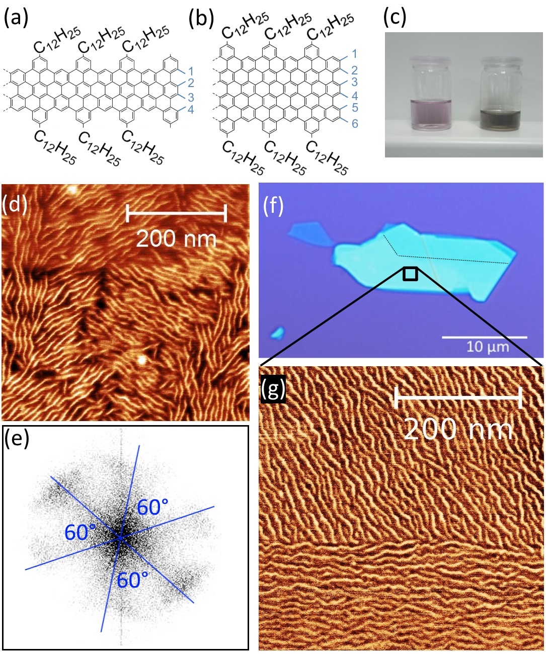
Subsequently, we exfoliated hBN on a Si/SiO2 chip, drop-cast the cGNR dispersion onto the chip, and evaporated the solvent by placing the chip onto a hot plate. Afterwards, we investigated the flakes with an atomic force microscope (AFM). Fig. 1 (d) and (h) show AFM phase images of 4- and 6-cGNRs, respectively, on hBN flakes. In previous studies on SiO2, it was found that cGNRs only absorb on carefully functionalized substratesAbbas et al. (2014); Zschieschang et al. (2015). Similarly, we did not observe cGNR adsorption on the untreated SiO2 surface on our samples. In contrast, we found that cGNRs adsorb readily to the atomically flat hBN surfaces and form well-ordered domains with domain sizes ranging from 60 nm to over 1 m and ribbon lengths of up to 350 nm. Length distributions for both cGNR types can be found in the Supplemental Material. The situation is similar to adsorption on highly-oriented pyrolitic graphite (HOPG) surfaces Narita et al. (2014), but with an important difference. While cGNRs on HOPG form arrays of straight ribbons, here we find that individual GNRs have a wiggled structure. Although we cannot offer a clear explanation for this observation, a possible reason could be the slight lattice mismatch between hBN and the graphene backbone of the cGNRs. This was shown in molecular dynamics simulations to lead to lateral buckling and snake-like motion of GNRs Ouyang et al. (2018). Alternatively, non-planar adsorption of the alkyl-side chains on the hBN could play a role. It should be further mentioned that the cGNRs seem to be very mobile on the hBN surface. cGNR covered hBN flakes were annealed to 450 ∘C and then re-investigated with AFM. Before, the hBN flake was homogeneously covered with cGNRs, after the annealing the cGNRs seem to have formed agglomerates (see Supplementary Material) and the bare hBN flake is visible again. The superlubricity of armchair GNRs on a gold substrate was already reported in UHV experiments.Kawai et al. (2016) Finally, we note that, although we assume that the cGNRs form monolayers on the hBN flakes, given the -resolution of our AFM we cannot rule out that more than one layer of cGNRs is adsorbed on the hBN. The ordered domains of cGNRs on hBN are found to be rotated by 60∘ with respect to each other. The angles between the domains become especially clear when we plot a two dimensional Fast Fourier Transformation (2D-FFT) of the AFM phase image (Fig. 1 (e)). The broadening of the 2D-FFT is mainly due to the wiggled structure of the cGNRs.
Fig. 1 (f) shows an optical microscope image of an exfoliated hBN flake on a Si/SiO2 chip before deposition of 6-cGNRs. When exfoliating hBN onto SiO2, it often cleaves along its crystallographic axes. Considering the hexagonal lattice structure of hBN consisting of alternating B and N atomsTaniguchi and Watanabe (2007), this yields cleaving angles in multiples of 30∘. Two of those axes are indicated with black dashed lines in Fig. 1 (f). Fig. 1 (g) is an AFM phase image of the area enclosed by the black square in Fig. 1 (f) after drop-casting the 6-cGNRs onto the chip. When comparing the orientation of the cGNRs in Fig. 1 (g) and the edges of the hBN flake in Fig. 1 (f), it becomes apparent that the cGNR domains are aligned along the crystallographic axes of the hBN.
Next, we contacted the cGNRs by performing electron beam lithography and evaporating metals (thermally and e-beam). NiCr/Au or PdXia et al. (2011) served as contact materials. Pd was deposited without any adhesion layer, therefore care had to be taken during lift-off not to damage the fine metal structures. We contacted multiple cGNRs at once, using interdigitated comb-like structures (see lower inset of Fig. 2). The orientation of the contact combs was chosen in such a way that the contacts were perpendicular to some of the cGNR domains. Fig. 2 shows an optical microscope image of one device with 15 nm thick Pd contacts.
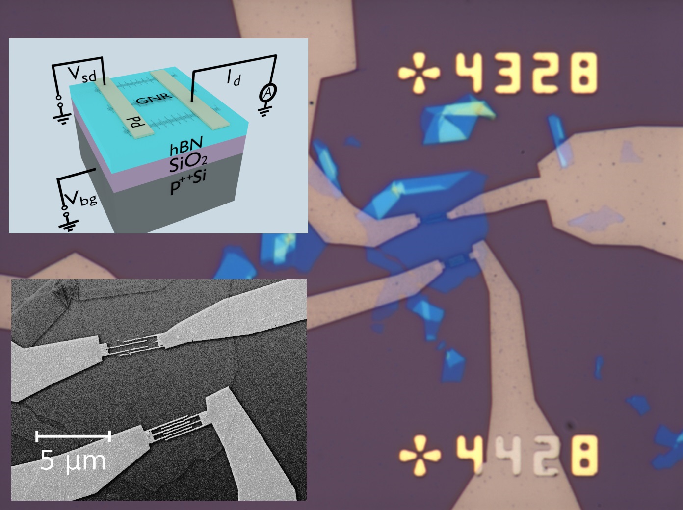
The schematics of the measurement setup is sketched in the upper inset of Fig. 2. With a probe station at ambient conditions, a source drain voltage was applied across the ribbons and the drain current was measured. The heavily p-doped Si substrate could be used as a back gate electrode by applying a back gate voltage . The SiO2 layer was 285 nm thick, the thickness of the used hBN flakes varied between 10-40 nm and the spacing of the contacts between 70-120 nm.
Fig. 3 shows --measurements of 4- and 6-cGNRs contacted with NiCr/Au and Pd. The NiCr/Au contacted 4-cGNRs (black squares) show a current onset for the lowest source drain voltages. We note that all curves are asymmetric with respect to . Possible sources for this asymmetry could be slightly different work functions of the electrodes due to contaminationPerello et al. (2011), different contact areasZhang et al. (2007), or the fact that the bias voltage is not applied symmetrically, but with one terminal grounded Appenzeller et al. (2002).
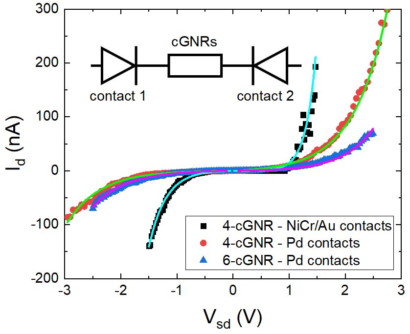
The Pd contacted 4- and 6-cGNRs look very similar on the negative voltage side and differ only slightly on the positive side. This is quite surprising since their different band gap should be reflected in the --curves. Here we assume that the Fermi level is always situated in the gap, as the curves can be described by a Schottky characteristic (see below). Further, when measuring contact pairs of further devices (of the same kind of cGNR and the same contact metal) the shape of the --curves deviated from the curves shown in Fig. 3 and also the drain currents varied even by orders of magnitudes (see, e.g., inset of Fig. 4). Taking all these effects into account, it seems likely that the measurements are dominated by the Schottky behavior of the contacts between the semiconducting cGNRs and the metallic electrodes. The transition from the metal to the cGNR and back to the metal can be seen as two back-to-back connected Schottky diodesChiquito et al. (2012); Sze and Ng (2007) with a resistor (one or many cGNRs) in between (see inset of Fig. 3). Since the detected current is limited by the current leaking through the Schottky diode in reverse direction, we fitted the Schottky barriers separately for negative and positive voltage regions (for the reverse direction of the Schottky diode). The slight difference in barrier height for positive and negative bias was included in the error margin. We found that the current density of our data is best described by the thermionic field emission model:Padovani and Stratton (1966); Zhang et al. (2007); Liu et al. (2008); Perello et al. (2011)
| (1) | |||||
Here, is the Richardson constant, the temperature, the height of the Schottky barrier, the Boltzmann constant, the elementary charge, the voltage applied across the barrier, and the distance between the band edge and the Fermi level. describes the shape of the barrierPadovani and Stratton (1966) and . For the contact area, we take the cross-sectional area of one nanoribbon, but include the unknown number of parallel ribbons, and further sources of uncertainty, in the error margin of (for more details, see the Supplemental Material).
| Sample | |||
|---|---|---|---|
| NiCr/Au 4-cGNR | meV | 16 mV | 0.15 V |
| Pd 4-cGNR | meV | 9 mV | 0.2 V |
| Pd 6-cGNR | meV | 9 mV | 0.2 V |
The fitting results are summarized in Table 1. NiCr/Au yields a higher barrier than the Pd contacts. Furthermore, Pd contacts worked more reliably than NiCr/Au contacts which is why no data are shown for NiCr/Au contacted 6-cGNRs. Taking these facts into account, Pd seems to be the better contact material. The above numbers, however, have to be considered with care. Strictly speaking, the Richardson constant is only valid for the free electron mass, but has to be modified using the electron effective mass Crowell (1965); Sze and Ng (2007), which is unknown for our contact configuration. We therefore used the free electron mass. Also, the alkyl side chains could partially overlap with the cGNRs,Narita et al. (2014) leading to a further increase of the contact resistance. Both uncertainties are absorbed in the error of the barrier height . The obtained values for are in line with earlier results on carbon nanotubes.Svensson and Campbell (2011)
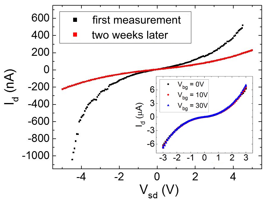
Additionally we studied the stability of our fabricated devices in air. Fig. 4 shows Pd contacted 6-cGNRs measured directly after fabrication (black squares) and two weeks later (red squares). The decreased drain current could be due to degradation of the cGNRs, degradation of the contacts, or contamination of the cGNRs by particles in the air.
Finally, we studied the gate response of our devices. As can be seen in the inset of Fig. 4, the devices showed (almost) no back gate dependence which could be due to Fermi level pinning at the Schottky contacts. Also, we note that the distance to the Si back gate is much larger than the separation of the metal electrodes. Therefore, we expect the gate coupling to be greatly reduced due to screening.
In previous studies, GNRs prepared from molecular precursors by either surface synthesisLlinas et al. (2017) or in solutionAbbas et al. (2014); Zschieschang et al. (2015), were deposited on oxidized silicon. When depositing 4-cGNRs dispersed in organic solvents or water onto SiO2, careful surface functionalization was necessaryAbbas et al. (2014); Konnerth et al. (2015); Zschieschang et al. (2015). In this work, on the other hand, cGNRs adsorb readily to the hBN surface. We found dense arrays of cGNRs on almost every hBN flake studied. This presents a clear advantage over the previous preparation method. In addition, hBN was shown to be a more suitable substrate for high-quality graphene devices. With respect to the contact transparency, we note that previous experiments on 4-cGNRs prepared from organic solvents and surface synthesized armchair GNRs found a device current in the 1 to 1000 nA range for a source-drain bias of 1 V, in line with our observations.Abbas et al. (2014); Fantuzzi et al. (2016); Llinas et al. (2017) This also holds for 6-cGNRs which were not previously used in transport devices. In the case of cGNRs prepared from aqueous solution, Zschieschang et al. obtained a drain current of tens of A. However, their devices showed signs of agglomeration, leading to a greatly reduced band gap, which could explain the lower Schottky barrier.Zschieschang et al. (2015)
In summary, we dispersed chemically synthesized 4- and 6-cGNRs in THF or cholorobenzene. The dispersion was drop-cast onto exfoliated hBN. cGNRs adsorb readily to the flat hBN surfaces and form ordered domains aligned along the crystallographic axes of the hBN, showing the potential of hBN as a substrate for GNR-based devices. We contacted the cGNRs with NiCr/Au, or Pd contacts. The --characteristics of the devices are dominated by the Schottky behavior of the contacts between metal and ribbon. Therefore, better contacts, such as edge-type contacts Matsuda et al. (2010); Wang et al. (2013); Huang et al. (2015) and local gates are called for, which are technologically more demanding.
Supplementary Material
See Supplementary Material for an AFM image comparing the cGNR coverage on SiO2 and hBN, for the effect of annealing, for the length distriution, for details on fitting the --curves and for an exemplary vs curve, showing no clear gate dependence.
Acknowledgements.
Financial support by the Deutsche Forschungsgemeinschaft (DFG) within the programs SFB 689, GRK 1570 and SPP1459 and by the Max Planck Society for the synthesis of cGNRs is gratefully acknowledged. Growth of hexagonal boron nitride crystals was supported by the Elemental Strategy Initiative conducted by the MEXT, Japan and JSPS KAKENHI Grant Numbers JP15K21722.References
- Schwierz (2010) F. Schwierz, Nature Nanotechnology 5, 487 (2010).
- Nakada et al. (1996) K. Nakada, M. Fujita, G. Dresselhaus, and M. S. Dresselhaus, Physical Review B 54, 17954 (1996).
- Han et al. (2007) M. Y. Han, B. Özyilmaz, Y. Zhang, and P. Kim, Physical Review Letters 98, 206805 (2007).
- Kosynkin et al. (2009) D. V. Kosynkin, A. L. Higginbotham, A. Sinitskii, J. R. Lomeda, A. Dimiev, B. K. Price, and J. M. Tour, Nature 458, 872 (2009).
- Jiao et al. (2009) L. Jiao, L. Zhang, X. Wang, G. Diankov, and H. Dai, Nature 458, 877 (2009).
- Han et al. (2010) M. Y. Han, J. C. Brant, and P. Kim, Physical Review Letters 104, 056801 (2010).
- Evaldsson et al. (2008) M. Evaldsson, I. V. Zozoulenko, H. Xu, and T. Heinzel, Physical Review B 78, 161407 (2008).
- Baringhaus et al. (2014) J. Baringhaus, M. Ruan, F. Edler, A. Tejeda, M. Sicot, A. Taleb-Ibrahimi, A.-P. Li, Z. Jiang, E. H. Conrad, C. Berger, C. Tegenkamp, and W. A. de Heer, Nature 506, 349 (2014).
- Chen et al. (2017) L. Chen, L. He, H. S. Wang, H. Wang, S. Tang, C. Cong, H. Xie, L. Li, H. Xia, T. Li, T. Wu, D. Zhang, L. Deng, T. Yu, X. Xie, and M. Jiang, Nature Communications 8, 14703 (2017).
- Cai et al. (2010) J. Cai, P. Ruffieux, R. Jaafar, M. Bieri, T. Braun, S. Blankenburg, M. Muoth, A. P. Seitsonen, M. Saleh, X. Feng, K. Müllen, and R. Fasel, Nature 466, 470 (2010).
- Bennett et al. (2013) P. B. Bennett, Z. Pedramrazi, A. Madani, Y.-C. Chen, D. G. de Oteyza, C. Chen, F. R. Fischer, M. F. Crommie, and J. Bokor, Applied Physics Letters 103, 253114 (2013).
- Chen et al. (2016) Z. Chen, W. Zhang, C.-A. Palma, A. Lodi Rizzini, B. Liu, A. Abbas, N. Richter, L. Martini, X.-Y. Wang, N. Cavani, H. Lu, N. Mishra, C. Coletti, R. Berger, F. Klappenberger, M. Kläui, A. Candini, M. Affronte, C. Zhou, V. De Renzi, U. del Pennino, J. V. Barth, H. J. Räder, A. Narita, X. Feng, and K. Müllen, Journal of the American Chemical Society 138, 15488 (2016).
- Llinas et al. (2017) J. P. Llinas, A. Fairbrother, G. Borin Barin, W. Shi, K. Lee, S. Wu, B. Yong Choi, R. Braganza, J. Lear, N. Kau, W. Choi, C. Chen, Z. Pedramrazi, T. Dumslaff, A. Narita, X. Feng, K. Müllen, F. Fischer, A. Zettl, P. Ruffieux, E. Yablonovitch, M. Crommie, R. Fasel, and J. Bokor, Nature Communications 8, 633 (2017).
- Narita et al. (2014) A. Narita, X. Feng, Y. Hernandez, S. A. Jensen, M. Bonn, H. Yang, I. A. Verzhbitskiy, C. Casiraghi, M. R. Hansen, A. H. R. Koch, G. Fytas, O. Ivasenko, B. Li, K. S. Mali, T. Balandina, S. Mahesh, S. De Feyter, and K. Müllen, Nature Chemistry 6, 126 (2014).
- Abbas et al. (2014) A. N. Abbas, G. Liu, A. Narita, M. Orosco, X. Feng, K. Müllen, and C. Zhou, Journal of the American Chemical Society 136, 7555 (2014).
- Zschieschang et al. (2015) U. Zschieschang, H. Klauk, I. B. Müller, A. J. Strudwick, T. Hintermann, M. G. Schwab, A. Narita, X. Feng, K. Müllen, and R. T. Weitz, Advanced Electronic Materials 1, 1400010 (2015).
- Fantuzzi et al. (2016) P. Fantuzzi, L. Martini, A. Candini, V. Corradini, U. del Pennino, Y. Hu, X. Feng, K. Müllen, A. Narita, and M. Affronte, Carbon 104, 112 (2016).
- Dean et al. (2010) C. R. Dean, A. F. Young, I. Meric, C. Lee, L. Wang, S. Sorgenfrei, K. Watanabe, T. Taniguchi, P. Kim, K. L. Shepard, and J. Hone, Nature Nanotechnology 5, 722 (2010).
- Bischoff et al. (2012) D. Bischoff, T. Krähenmann, S. Dröscher, M. A. Gruner, C. Barraud, T. Ihn, and K. Ensslin, Applied Physics Letters 101, 203103 (2012).
- Hu et al. (2018) Y. Hu, P. Xie, M. De Corato, A. Ruini, S. Zhao, F. Meggendorfer, L. A. Straasø, L. Rondin, P. Simon, J. Li, J. J. Finley, M. R. Hansen, J.-S. Lauret, E. Molinari, X. Feng, J. V. Barth, C.-A. Palma, D. Prezzi, K. Müllen, and A. Narita, J. Am. Chem. Soc. 140, 7803 (2018).
- Osella et al. (2012) S. Osella, A. Narita, M. G. Schwab, Y. Hernandez, X. Feng, K. Müllen, and D. Beljonne, ACS Nano 6, 5539 (2012).
- Ivanov et al. (2017) I. Ivanov, Y. Hu, S. Osella, U. Beser, H. I. Wang, D. Beljonne, A. Narita, K. Müllen, D. Turchinovich, and M. Bonn, J. Am. Chem. Soc. 139, 7982 (2017).
- Villegas et al. (2014) C. E. P. Villegas, P. B. Mendonça, and A. R. Rocha, Scientific Reports 4, 6579 (2014).
- Ouyang et al. (2018) W. Ouyang, D. Mandelli, M. Urbakh, and O. Hod, Nano Letters 18, 6009 (2018).
- Kawai et al. (2016) S. Kawai, A. Benassi, E. Gnecco, H. Söde, R. Pawlak, X. Feng, K. Müllen, D. Passerone, C. A. Pignedoli, P. Ruffieux, R. Fasel, and E. Meyer, Science 351, 957 (2016).
- Taniguchi and Watanabe (2007) T. Taniguchi and K. Watanabe, Journal of Crystal Growth 303, 525 (2007).
- Xia et al. (2011) F. Xia, V. Perebeinos, Y.-m. Lin, Y. Wu, and P. Avouris, Nature Nanotechnology 6, 179 (2011).
- Perello et al. (2011) D. J. Perello, S. C. Lim, S. J. Chae, I. Lee, M. J. Kim, Y. H. Lee, and M. Yun, ACS Nano 5, 1756 (2011).
- Zhang et al. (2007) Z. Zhang, K. Yao, Y. Liu, C. Jin, X. Liang, Q. Chen, and L.-M. Peng, Adv. Funct. Mater. 17, 2478 (2007).
- Appenzeller et al. (2002) J. Appenzeller, J. Knoch, V. Derycke, R. Martel, S. Wind, and P. Avouris, Phys. Rev. Lett. 89, 126801 (2002).
- Chiquito et al. (2012) A. J. Chiquito, C. A. Amorim, O. M. Berengue, L. S. Araujo, E. P. Bernardo, and E. R. Leite, Journal of Physics: Condensed Matter 24, 225303 (2012).
- Sze and Ng (2007) S. M. Sze and K. K. Ng, Physics of Semiconductor Devices, 3rd ed. (John Wiley & Sons, 2007).
- Padovani and Stratton (1966) F. A. Padovani and R. Stratton, Solid-State Electronics 9, 695 (1966).
- Liu et al. (2008) Y. Liu, Z. Y. Zhang, Y. F. Hu, C. H. Jin, and L.-M. Peng, J. Nanosc. Nanotechnol. 8, 252 (2008).
- Crowell (1965) C. Crowell, Solid-State Electronics 8, 395 (1965).
- Svensson and Campbell (2011) J. Svensson and E. E. B. Campbell, Journal of Applied Physics 110, 111101 (2011).
- Konnerth et al. (2015) R. Konnerth, C. Cervetti, A. Narita, X. Feng, K. Müllen, A. Hoyer, M. Burghard, K. Kern, M. Dressel, and L. Bogani, Nanoscale 7, 12807 (2015).
- Matsuda et al. (2010) Y. Matsuda, W.-Q. Deng, and W. A. Goddard, J. Phys. Chem. C 114, 17845 (2010).
- Wang et al. (2013) L. Wang, I. Meric, P. Y. Huang, Q. Gao, Y. Gao, H. Tran, T. Taniguchi, K. Watanabe, L. M. Campos, D. A. Muller, J. Guo, P. Kim, J. Hone, K. L. Shepard, and C. R. Dean, Science 342, 614 (2013).
- Huang et al. (2015) J.-W. Huang, C. Pan, S. Tran, B. Cheng, K. Watanabe, T. Taniguchi, C. N. Lau, and M. Bockrath, Nano Letters 15, 6836 (2015).