Quantum transport properties of industrial 28Si/28SiO2
Abstract
We investigate the structural and quantum transport properties of isotopically enriched 28Si/28SiO2 stacks deposited on 300 mm Si wafers in an industrial CMOS fab. Highly uniform films are obtained with an isotopic purity greater than 99.92%. Hall-bar transistors with an equivalent oxide thickness of 17 nm are fabricated in an academic cleanroom. A critical density for conduction of cm-2 and a peak mobility of 9800 cm2/Vs are measured at a temperature of 1.7 K. The 28Si/28SiO2 interface is characterized by a roughness of nm and a correlation length of nm. An upper bound for valley splitting energy of 480 eV is estimated at an effective electric field of 9.5 MV/m. These results support the use of wafer-scale 28Si/28SiO2 as a promising material platform to manufacture industrial spin qubits.
Enrichment of the spin-zero 28Si isotope drastically reduces spin-bath decoherence in silicon Witzel et al. (2010); Witzel and Das Sarma (2006) and has enabled solid state spin qubits with extremely long coherence Muhonen et al. (2014); Veldhorst et al. (2015) and high control fidelity Veldhorst et al. (2014); Yoneda et al. (2018); Huang et al. (2018). The limited availability of isotopically enriched 28Si in industrially adopted forms Itoh and Watanabe (2014), however, was previously thought to be a major bottleneck to leverage CMOS technology for manufacturing qubits with the quality and in the large numbers required for fault tolerant quantum computation Vandersypen et al. (2017); Li et al. (2018). Recently, isotopically enriched silane (28SiH4) has been employed in a pre-industrial CMOS facility to deposit high quality 28Si epi-wafers Mazzocchi et al. (2019). Crucially, an industrial supply of 28SiH4 has been established and silicon quantum dots were fabricated on a wafer-scale 28Si/28SiO2 stack grown in an industrial manufacturing CMOS fab Petit et al. (2018). In these quantum dots, a single-electron spin lifetime of 2.8 ms was obtained at a temperature of 1.1 K and weak charge noise was measured, pointing to a promising material platform for qubit operation at elevated temperatures.
Studies devoted to 28Si quantum dots, however, tend to discuss only marginally the structural properties of the originating 28Si/28SiO2 material stack and the electrical transport in the associated two-dimensional electron gas (2DEG). In this paper we provide structural characterization of the same industrial 28Si wafer used for quantum dots in Ref. Petit et al. (2018) and assess the disorder properties of the critical 28Si/28SiO2 interface. By investigating the quantum transport properties of Hall-bar transistors, we extract key material metrics such as carrier mobility, critical density, interface roughness, interface correlation length, and valley splitting energy. Electron mobility is typically used as a figure of merit to assess the quality of the semiconductor/oxide interface. However, peak mobility is measured at high electron density, where screening effects are relevant Tracy et al. (2009); Kim et al. (2017). The critical density, instead, indicates the minimum density required to establish metallic conduction by overcoming electron trapping at the oxide interface. As such, the critical density is a complementary metric to the mobility and characterizes the interface disorder at low densities, where quantum devices typically operate. Overall, large mobility and small critical density indicate material uniformity and low disorder at the confining interfaces. These properties are beneficial for obtaining reproducible quantum dots at intended locations on the substrate. Valley splitting quantifies the energetic separation between the ground state used for computation and the lowest excited state. A sharp flat interface is required to achieve large splitting energy, which is beneficial for qubit operation Culcer et al. (2010); Yang et al. (2013). The results reported in this work indicate a low disorder environment at the 28Si/28SiO2 interface and potential to achieve large valley splitting, supporting the industrial integration of spin qubits on wafer-scale 28Si.
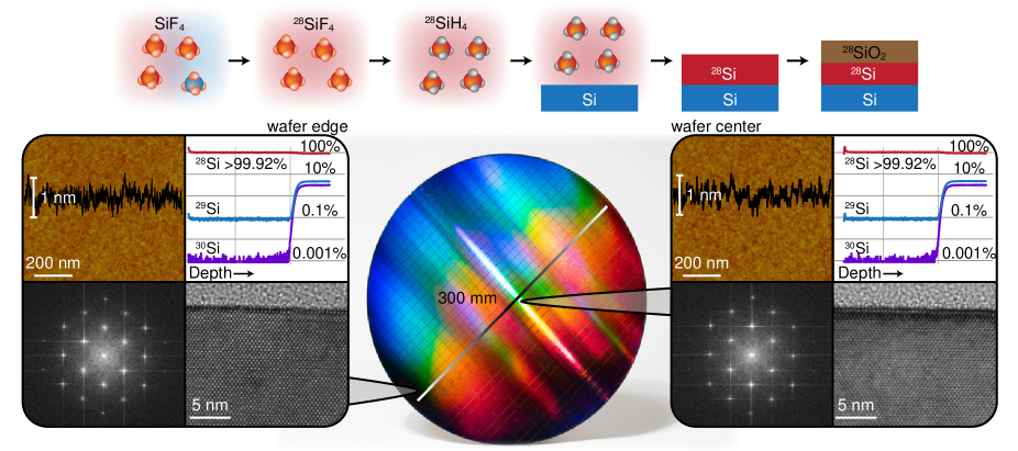
The schematics in Fig. 1 illustrate the key steps in the supply chain of isotopically enriched precursors for wafer-scale epitaxial growth of 28Si. A silicon-tetrafluoride gas (SiF4) with natural abundance of 28Si of 92.23% is isotopically enriched in 28Si to a concentration greater than 99.92% by centrifuge separation. The 28SiF4, with a residual 29Si concentration of 0.08%, is then reduced to obtain high purity 28SiH4. 28SiH4 gas cylinders have been installed for use in a state-of-the-art chemical vapour deposition tool of a 300 mm fabrication line to deposit 28Si epilayers. Maintaining the chemical purity of gas precursors throughout the supply chain is crucial to obtain a low-disorder 28Si/28SiO2 stack. The growth process starts with the deposition of 1 m of intrinsic natural Si on a high-resistivity 300 mm Si(100) wafer followed by a 100-nm-thick intrinsic 28Si epilayer. The wafer is then thermally processed at high temperature for the formation of a high quality 10-nm-thick 28SiO2 layer.
In Fig. 1 we compare morphology and composition of the grown stack at the center and the edge of the 300 mm wafer. No difference in surface or interface roughness, composition, and purity could be observed across the wafer, indicating a uniform film deposition. Atomic force microscopy shows a uniform and near defect-free surface with a root mean square surface roughness of 0.2 nm. Secondary ion mass spectroscopy of isotopes 28Si, 29Si, and 30Si shows a high purity film with a residual concentration of non-zero-spin nuclei 29Si reduced from in the Si buffer to in the purified epilayer, demonstrating that the precursor purity has been preserved during the deposition process. The concentration of common background contaminants C and O is below the detection limit of cm-3 and cm-3, respectively. High-resolution transmission electron microscopy shows that no dislocations or stacking faults are visible in the epilayer. Moreover, the 28Si/28SiO2 interface is flat down to 1-2 atomic layers over distances (nm) that are larger than the typical size of Si quantum dot spin qubits. The sharpness of the interface, the negligible density of defects in the lattice, and the associated electron diffraction pattern highlight the film quality and the good control over the growth process attained in a manufacturing CMOS fab.
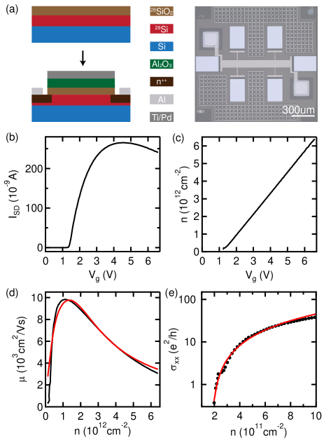
Moving on to device fabrication, Fig. 2(a) shows schematics and optical micrograph of a MOS transistor shaped in a Hall-bar geometry to investigate the magnetotransport properties of the 2DEG at the 28Si/28SiO2 interface. The device was fabricated in an academic cleanroom environment, starting from coupon-sized samples diced from the original 28Si/28SiO2 300 mm wafer. We employ e-beam lithography and lift-off additive techniques to resemble the process flow used to fabricate quantum dots as in Ref. Petit et al. (2018). Highly doped n++ regions are obtained by P-ion implantation followed by 30 s of activation anneal at 1000∘C in N2 environment. Multiple ohmic contacts are deposited on the implant regions by e-beam evaporation of Al. An additional Al2O3 layer was deposited by atomic layer deposition at 300∘C, so that the 28Si/28SiO2 interface undergoes similar processing as in the fabrication of multi-layer gate-defined qubits Petit et al. (2018). The resulting dielectric stack has an equivalent oxide thickness (EOT) of 17 nm. A Ti/Pd top gate is deposited to define a Hall-bar geometry with a 100-m-wide and 500-m-long central region. The last processing step is a forming gas anneal at 400∘C to reduce the damage induced by e-beam lithography Nordberg et al. (2009); Kim et al. (2017).
The electrical characterization of the device was performed at a temperature of 1.7 K using standard four-terminal low frequency lock-in techniques with a constant source-drain excitation voltage of 1 mV. Longitudinal () and transverse () resistivity were measured as a function of carrier density - controlled by the top gate - and external perpendicular magnetic field . The Hall carrier density and the electron mobility are calculated using the relationships and , respectively, where is the elementary charge and T).
A DC voltage applied to the top gate () accumulates a 2DEG at the 28Si/28SiO2 interface which conducts above a turn-on voltage of = 1.22 V, as shown in Fig. 2(b). For values below no current flow is observed in the device up to a temperature of K, confirming the insulating behavior of the intrinsic 28Si film at low temperature. For (Fig. 2(c)) we measure a linear increase in the Hall density as a function of . The experimental capacitance = F/cm2 matches within 5% the expected value for the given EOT. Upon multiple sweeps of no hysteresis is observed and the same values of and are measured, indicating a stable potential landscape at the oxide interface.
The experimental and theoretically calculated density-dependent mobility curves are shown in Fig. 2(d). Above a critical density, required to establish metallic conduction in the 2DEG, the mobility rises sharply due to screening from charged impurity Coulomb scattering Ando et al. (1982); Gold (1985); Gold and Dolgopolov (1986); Kruithof et al. (1991). A peak mobility of 9800 cm2/Vs is reached at cm-2, corresponding to a mean free path of 120 nm. Beyond, the mobility drops due to surface roughness scattering at the 28Si/28SiO2 interface Ando et al. (1982); Gold and Dolgopolov (1986); Kruithof et al. (1991). The calculated scattering-limited mobility takes into account a scattering charge density at the semiconductor/oxide interface and an exponential autocorrelation function form of the interface roughness Gold and Dolgopolov (1986); Kruithof et al. (1991); Tracy et al. (2009). A good match is obtained for a scattering charge density of cm-2, an interface roughness of nm, and an interface correlation length of nm. describes the interface root-mean-square height fluctuations, is the lateral distance over which the fluctuations are correlated. The interface roughness is compatible with the morphology investigation by transmission electron microscopy reported in Fig. 1.
| Reference | This work | Ref. Rochette et al. (2017) | Ref. Shankar et al. (2010) | Ref. Nordberg et al. (2009) | Ref. Kim et al. (2017) | Ref. Kim et al. (2017) | Ref. Tracy et al. (2009) | Ref. Tracy et al. (2009) |
|---|---|---|---|---|---|---|---|---|
| Channel material | 99.92% 28Si-epi | 99.95% 28Si-epi | 28Si-epi | Si bulk | Si bulk | Si bulk | Si bulk | Si bulk |
| Equivalent oxide thickness (nm) | 17 | 35 | 110 | 62 | 35 | 35 | 30 | 10 |
| E-beam exposure/forming gas | Yes | N/A | N/A | Yes | Yes | No | No | No |
| Mobility (103 cm2/Vs) | 9.8 | 11.6 | 14 | 8.3 | 14 | 23 | 15 | 10 |
| Critical density (1011 cm-2) | 1.75 | 1.60 | N/A | N/A | 0.95111Percolation transition density extrapolated at . | 0.8311footnotemark: 1 | 1.0411footnotemark: 1 | N/A |
| Quantum dot fabrication | Yes Petit et al. (2018) | Yes | No | Yes | No | No | No | No |
The critical density is extracted from a percolation fit of the density-dependent conductivity (Fig. 2(e)) Kim et al. (2017); Tracy et al. (2009), where , are the percolation transition density and exponent, respectively. By fixing , as expected in a 2D system, we estimate cm-2 at K. Previous studies have shown that decreases with decreasing temperature Kim et al. (2017); Tracy et al. (2009), therefore the obtained value of cm-2 sets an upper bound for the critical density in the temperature regime at which qubits are typically operated ( mK).
Both the mobility and critical density obtained in wafer-scale isotopically enriched 28Si/28SiO2 stack are qualitatively comparable to the values previously reported for high-mobility Si MOSFETs at low temperatures Rochette et al. (2017); Shankar et al. (2010); Kim et al. (2017); Nordberg et al. (2009); Tracy et al. (2009) (see Table 1). In drawing a meaningful comparison with the data reported in the literature, the reader should consider samples with similar EOT and device process flow. In fact, the mobility is known to be higher in devices with thicker oxide Ando et al. (1982); Yagi and Kawaji (1978) and degrades upon device exposure to electron-beam Nordberg et al. (2009); Kim et al. (2017).
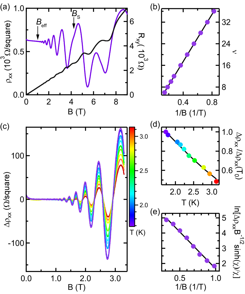
Transport characterization at high magnetic field (Fig. 3) allows the measurement of effective mass and quantum lifetime , from which we estimate an upper bound for the valley splitting energy and the -factor. In Fig. 3(a) we report the longitudinal magnetoresistivity at a density cm-2 which corresponds to an effective electric field of 9.5 MV/m. Shubnikov-de Haas (SdH) oscillations are observed, with minima aligned to quantum Hall plateaus in . SdH oscillations start at T and spin degeneracy is resolved at T, corresponding to the even filling factor . Figure 3(b) shows the filling factor progression against . High mobility and density allow to resolve filling factors up to , with fourfold periodicity at low magnetic field due to spin and valley degeneracy and twofold periodicity beyond . We do not observe odd filling factors, indicating that twofold valley degeneracy is not resolved under these measurement conditions. From the linear filling factor progression we extract a density cm-2. The agreement between the Hall density and indicates that only one high-mobility subband contributes to electrical transport, confirming the high quality 28Si epitaxy.
The transverse effective mass of the high mobility carriers is calculated from the damping of the SdH oscillations with increasing temperature, described by the relation Bauer and Kahlert (1972); Isihara and Smrcka (1986); Coleridge (1991); Celik et al. (2011)
| (1) |
where is the SdH oscillation amplitude after polynomial background subtraction, , , is the cyclotron frequency, is the Planck constant, and the Boltzmann constant. Figure 3(d) shows the temperature dependence of the oscillation amplitude at T, before spin-splitting, normalized to the amplitude at K. By fitting the data to Eq. 1 we obtain an effective mass of , where is the free-electron mass, and a transport lifetime ps. The value is in agreement with measurements performed on natural Si Fang et al. (1977) and corresponds to the expected value obtained from band structure calculations neglecting many-body effects Ando et al. (1982).
Once the effective mass is measured, the quantum lifetime can be determined from the SdH oscillation envelope at , using the relation Bauer and Kahlert (1972); Celik et al. (2011)
| (2) |
The Dingle plot of Fig. 3(e) reports the fit from which we extract ps. The obtained implies a Landau level broadening of eV, which sets an upper bound to valley splitting at the investigated density (electric field) and magnetic field. For comparison, a valley splitting energy of 275 eV was measured in 28Si quantum dots fabricated on the same wafer in an academic environment Petit et al. (2018). The electron -factor is evaluated by considering that the onset of spin-splitting at implies a Zeeman energy , where is the Bohr magneton. From this, a -factor of is estimated, which is close to the expected single-particle value of .
In conclusion, we investigated the structural and quantum transport properties of isotopically enriched 28Si/28SiO2 stacks deposited on 300 mm wafers in an industrial CMOS fab. The material characterization shows that the level of control achieved in the growth process results in a uniform deposition with high purity epilayers and a sharp semiconductor/oxide interface. Detailed quantum transport characterization of Hall-bar devices fabricated in an academic cleanroom points to a high-quality 28Si/28SiO2 interface, promising for hosting spin qubits. Mobility and critical density for these stacks are among the best reported for equivalent oxide thicknesses, with the potential to achieve large valley splitting. Disorder at the critical semiconductor/oxide interface is expected to further decrease by processing the entire gate stack in the high volume manufacturing environment, because an advanced process control is attainable and e-beam induced damage is avoided.
Acknowledgements
M.V. acknowledges support from the Netherlands Organisation of Scientific Research (NWO) Vidi program. L.M.K.V., M.V. and G.S. acknowledge financial support by Intel Corporation.
References
- Witzel et al. (2010) W. M. Witzel, M. S. Carroll, A. Morello, L. Cywiński, and S. Das Sarma, Physical Review Letters 105, 187602 (2010).
- Witzel and Das Sarma (2006) W. M. Witzel and S. Das Sarma, Physical Review B 74, 035322 (2006).
- Muhonen et al. (2014) J. T. Muhonen, J. P. Dehollain, A. Laucht, F. E. Hudson, R. Kalra, T. Sekiguchi, K. M. Itoh, D. N. Jamieson, J. C. McCallum, A. S. Dzurak, and A. Morello, Nature Nanotechnology 9, 986 (2014).
- Veldhorst et al. (2015) M. Veldhorst, C. H. Yang, J. C. C. Hwang, W. Huang, J. P. Dehollain, J. T. Muhonen, S. Simmons, A. Laucht, F. E. Hudson, K. M. Itoh, A. Morello, and A. S. Dzurak, Nature 526, 410 (2015).
- Veldhorst et al. (2014) M. Veldhorst, J. C. C. Hwang, C. H. Yang, A. W. Leenstra, B. de Ronde, J. P. Dehollain, J. T. Muhonen, F. E. Hudson, K. M. Itoh, A. Morello, and A. S. Dzurak, Nature Nanotechnology 9, 981 (2014).
- Yoneda et al. (2018) J. Yoneda, K. Takeda, T. Otsuka, T. Nakajima, M. R. Delbecq, G. Allison, T. Honda, T. Kodera, S. Oda, Y. Hoshi, N. Usami, K. M. Itoh, and S. Tarucha, Nature Nanotechnology 13, 102 (2018).
- Huang et al. (2018) W. Huang, C. H. Yang, K. W. Chan, T. Tanttu, B. Hensen, R. C. C. Leon, M. A. Fogarty, J. C. C. Hwang, F. E. Hudson, K. M. Itoh, A. Morello, A. Laucht, and A. S. Dzurak, arXiv:1805.05027 (2018).
- Itoh and Watanabe (2014) K. M. Itoh and H. Watanabe, MRS Communications 4, 143 (2014).
- Vandersypen et al. (2017) L. M. K. Vandersypen, H. Bluhm, J. S. Clarke, A. S. Dzurak, R. Ishihara, A. Morello, D. J. Reilly, L. R. Schreiber, and M. Veldhorst, npj Quantum Information 3, 34 (2017).
- Li et al. (2018) R. Li, L. Petit, D. P. Franke, J. P. Dehollain, J. Helsen, M. Steudtner, N. K. Thomas, Z. R. Yoscovits, K. J. Singh, S. Wehner, L. M. K. Vandersypen, J. S. Clarke, and M. Veldhorst, Science Advances 4, eaar3960 (2018).
- Mazzocchi et al. (2019) V. Mazzocchi, P. G. Sennikov, A. D. Bulanov, M. F. Churbanov, B. Bertrand, L. Hutin, J. P. Barnes, M. N. Drozdov, J. M. Hartmann, and M. Sanquer, Journal of Crystal Growth 509, 1 (2019).
- Petit et al. (2018) L. Petit, J. M. Boter, H. G. J. Eenink, G. Droulers, M. L. V. Tagliaferri, R. Li, D. P. Franke, K. J. Singh, J. S. Clarke, R. N. Schouten, V. V. Dobrovitski, L. M. K. Vandersypen, and M. Veldhorst, Physical Review Letters 121, 076801 (2018).
- Tracy et al. (2009) L. A. Tracy, E. H. Hwang, K. Eng, G. A. Ten Eyck, E. P. Nordberg, K. Childs, M. S. Carroll, M. P. Lilly, and S. Das Sarma, Physical Review B 79, 235307 (2009).
- Kim et al. (2017) J.-S. Kim, A. M. Tyryshkin, and S. A. Lyon, Applied Physics Letters 110, 123505 (2017).
- Culcer et al. (2010) D. Culcer, X. Hu, and S. Das Sarma, Physical Review B 82, 205315 (2010).
- Yang et al. (2013) C. H. Yang, A. Rossi, R. Ruskov, N. S. Lai, F. A. Mohiyaddin, S. Lee, C. Tahan, G. Klimeck, A. Morello, and A. S. Dzurak, Nature Communications 4, 2069 (2013).
- Nordberg et al. (2009) E. P. Nordberg, G. A. Ten Eyck, H. Stalford, R. P. Muller, R. W. Young, K. Eng, L. A. Tracy, K. D. Childs, J. R. Wendt, R. K. Grubbs, J. Stevens, M. P. Lilly, M. A. Eriksson, and M. S. Carroll, Physical Review B 80, 115331 (2009).
- Ando et al. (1982) T. Ando, A. B. Fowler, and F. Stern, Reviews of Modern Physics 54, 437 (1982).
- Gold (1985) A. Gold, Physical Review Letters 54, 1079 (1985).
- Gold and Dolgopolov (1986) A. Gold and V. T. Dolgopolov, Physical Review B 33, 1076 (1986).
- Kruithof et al. (1991) G. H. Kruithof, T. M. Klapwijk, and S. Bakker, Physical Review B 43, 6642 (1991).
- Rochette et al. (2017) S. Rochette, M. Rudolph, A.-M. Roy, M. Curry, G. Ten Eyck, R. Manginell, J. Wendt, T. Pluym, S. M. Carr, D. Ward, M. P. Lilly, M. S. Carroll, and M. Pioro-Ladrière, arXiv:1707.03895 (2017).
- Shankar et al. (2010) S. Shankar, A. Tyryshkin, J. He, and S. Lyon, Physical Review B 82, 195323 (2010).
- Yagi and Kawaji (1978) A. Yagi and S. Kawaji, Applied Physics Letters 33, 349 (1978).
- Bauer and Kahlert (1972) G. Bauer and H. Kahlert, Physical Review B 5, 566 (1972).
- Isihara and Smrcka (1986) A. Isihara and L. Smrcka, Journal of Physics C: Solid State Physics 19, 6777 (1986).
- Coleridge (1991) P. T. Coleridge, Physical Review B 44, 3793 (1991).
- Celik et al. (2011) O. Celik, E. Tiras, S. Ardali, S. B. Lisesivdin, and E. Ozbay, Physica Status Solidi C 8, 1625 (2011).
- Fang et al. (1977) F. F. Fang, A. B. Fowler, and A. Hartstein, Physical Review B 16, 4446 (1977).