Towards the insulator-to-metal transition at the surface of ion-gated nanocrystalline diamond films
Abstract
Hole doping can control the conductivity of diamond either through boron substitution, or carrier accumulation in a field-effect transistor. In this work, we combine the two methods to investigate the insulator-to-metal transition at the surface of nanocrystalline diamond films. The finite boron doping strongly increases the maximum hole density which can be induced electrostatically with respect to intrinsic diamond. The ionic gate pushes the conductivity of the film surface away from the variable-range hopping regime and into the quantum critical regime. However, the combination of the strong intrinsic surface disorder due to a non-negligible surface roughness, and the introduction of extra scattering centers by the ionic gate, prevents the surface accumulation layer to reach the metallic regime.
Diamond is a promising material for electronic applications thanks to its wide band gap, large carrier mobility, high thermal conductivity and good electrochemical properties PanBook1995 . When boron (B) is substituted to carbon in the lattice structure, diamond becomes a p-type conductor and eventually a superconductor with a critical temperature K EkimovNature2004 ; BustarretPSS2008 , which can be further enhanced by optimizing the growth process TakanoAPL2004 ; OkazakiAPL2015 . Diamond is also considered a candidate for high-temperature superconductivity (SC) BoeriPRL2004 ; LeePRL2004 ; BoeriJPCS2005 ; GiustinoPRL2007 ; NakamuraPRB2013 thanks to its very large Debye temperature , but its attainability is hampered by disorder and the maximum B solubility BustarretPSS2008 ; TakanoAPL2004 ; OkazakiAPL2015 . Charge carriers can also be introduced in an insulator via the electric field effect in the form of a 2-dimensional (2D) surface accumulation layer, upon application of a transverse electric field. The electric-double-layer (EDL) transistor is a particularly effective field-effect architecture, thanks to the large electric field that develops at a solid/electrolyte interface when a voltage drop is applied across it UenoReview2014 . The electric transport properties of diamond-based EDL transistors have been extensively studied DankerlPRL2011 ; DankerlAPL2012 ; YamaguchiJPSJ2013 ; TakahidePRB2014 ; TakahidePRB2016 ; AkhgarNanoLett2016 , but no evidence was reported for either SC or good metallic behavior. This can be associated with the relatively modest charge carrier densities achieved in these works on insulating single crystals and epitaxial thin films ( cm-2 DankerlPRL2011 ; DankerlAPL2012 ; YamaguchiJPSJ2013 ; TakahidePRB2014 ; TakahidePRB2016 ; AkhgarNanoLett2016 ) with respect to the values typically obtained in conducting systems ( cm-2 DagheroPRL2012 ; TortelloApsusc2013 ; PiattiPRB2017 ; PiattiArXiv2018 ; GonnelliSciRep2015 ; PiattiJSNM2016 ; LiNature2016 ).
In this work, we focus on nanocrystalline diamond films and employ ionic gating to tune their surface conductivity via electrostatic hole doping. The films are slightly B-doped in order to provide a finite carrier density even in absence of an applied gate bias, and we show that this enhances the maximum induced hole density by a factor with respect to earlier reports. Despite this improvement, we don’t observe SC or good metallic behavior down to K. Instead, charge transport in the accumulation layer (AL) at the film surface moves from the variable-range hopping regime at low hole doping, into the quantum critical (QC) regime at high hole doping, never crossing into the metallic side of the insulator-to-metal transition (MIT). We propose that this frustrated behavior is associated to a combination of non-negligible surface roughness and additional scattering centers introduced by the ions in the EDL.
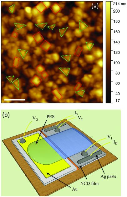
Nanocrystalline diamond (NCD) films were grown by a two-step Chemical Vapor Deposition (CVD) process on AF32eco high-temperature glass substrates. A detailed description of the growth process has been reported elsewhere PippionePSS2017 . The films consisted of an underlying intrinsic NCD layer () with a B-doped NCD layer ( nm) on top, as determined by Scanning Electron Microscopy PippionePSS2017 . Fig.1a shows a representative topography image acquired via Atomic Force Microscopy (AFM) in contact mode. The sample is polycrystalline with an average lateral grain size of nm. The largest grains typically grew in either rectangular (dashed red lines) or triangular (dashed green lines) shapes, which can be associated to - and -oriented facets respectively UshizawaDRM1998 . The average mean square roughness is nm, and the rugosity – defined as the ratio between the real and projected areas of the surface – is . The amount of B doping was estimated by Hall effect experiments performed in the van der Pauw configuration at room temperature, applying a magnetic field up to T with a calibrated permanent magnet. The resulting free holonic density was e+/cm3, corresponding to a B-doping concentration of %, and consistent with Ref.PippionePSS2017 .

Fig.1b shows a sketch of the EDL device, which was obtained by dicing the NCD film into smaller rectangles ( cm2), and drop-casting a small amount of conductive silver paste to realize electrical contacts for source (), drain (), and four-wire voltage probes ( and ). The EDL transistor was completed by drop-casting the liquid precursor to the cross-linked polymer electrolyte system (PES) on top of the active channel of the device – defined by the two voltage contacts – and the gold side gate (). The PES consisted of a mixture of BEMA dimethacrylate oligomer and EMIM-TFSI ionic liquid in 2:8 ratio along with 3 wt% of photo initiator, and was subsequently UV-cured in a dry room.
We measured the four-wire resistance as a function of temperature in the high-vacuum chamber ( mbar) of a pulse-tube cryocooler with a base K, by sourcing a probe DC current of few and measuring the longitudinal voltage drop across the active channel. Common mode offsets were eliminated with the current reversal method. We applied at K, slightly above the glass transition of the PES, in order to minimize the chance of electrochemical interactions between the sample and the electrolyte. For each application, the induced charge density is , where is the surface area of the NCD film covered by the PES, is the rugosity determined via AFM, and is the charge stored in the EDL as measured by double-step chronocoulometry. This is a well-established electrochemical technique InzeltBook which has been employed to reliably determine for a wide variety of materials DagheroPRL2012 ; TortelloApsusc2013 ; PiattiPRB2017 ; PiattiArXiv2018 ; GonnelliSciRep2015 ; PiattiJSNM2016 .


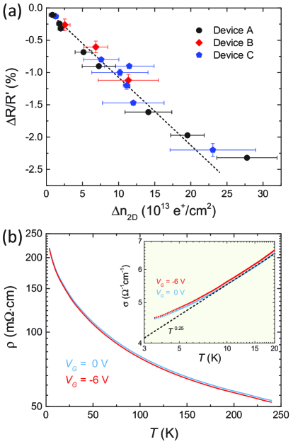
At constant K, applying increased the conductivity of our devices, while applying suppressed it. All modulations were entirely reversible by simply applying . These features indicate that tunes the conductivity by means of purely electrostatic accumulation/depletion of holonic charge carriers in the valence band of the NCD film. In the following, we concentrate on hole accumulation (). Fig.2a shows the normalized resistance variation as a function of at K for three different NCD devices. Horizontal and vertical error bars indicate the difference in the values of and determined between the charge and discharge of the EDL capacitor respectively. The maximum values of are more than times larger than the ones in earlier reports DankerlPRL2011 ; DankerlAPL2012 ; YamaguchiJPSJ2013 ; TakahidePRB2014 ; TakahidePRB2016 ; AkhgarNanoLett2016 . The negative slope of for increasing hole density indicates that charge transport is dominated by holonic carriers, consistent with the preliminary Hall measurements on the pristine film. Up to , shows a good linear scaling with , which is expected when the gate-induced modulation to the conductivity is dominated by electrostatic charge doping DagheroPRL2012 ; TortelloApsusc2013 ; PiattiPRB2017 ; PiattiArXiv2018 .
Fig.2b shows the -dependent resistivity at (blue curve) and V (red curve) in semilogarithmic scale. In both cases, decreases with increasing , which may suggest a semiconducting behavior. However, tends to saturate below K, which is the hallmark of a disordered metal McMillanPRB1981 ; LarkinJETP1982 ; HeegerPS2002 . This is best shown by plotting the -dependence of below K in double logarithmic scale (see the inset to Fig.2b). Between and K, at scales well with a power law , with ; below K, is larger than predicted by the scaling law and shows an incipient saturation. This indicates that, even at , the bulk charge transport is in the QC regime just on the metallic side of the MIT McMillanPRB1981 ; LarkinJETP1982 ; HeegerPS2002 . This is consistent with the pristine carrier concentration determined by Hall effect ( e+/cm3), as the bulk MIT occurs at a slighly lower doping e+/cm3 PippionePSS2017 ; GononJAP1995 . Since the induction of additional charge carriers in the system ( V) reduces /increases in the entire range without an obvious change in the scaling at low (see the inset to Fig.2b), the total is completely dominated by the bulk contribution for any .
We disentangle the charge transport of the gate-induced AL at the surface from the predominant bulk contribution through the method described in Ref.KounoArXiv2018 . For each value of , we define the sheet conductance of the AL, , as the difference between the total sheet conductance of the film, , at finite and at :
| (1) |
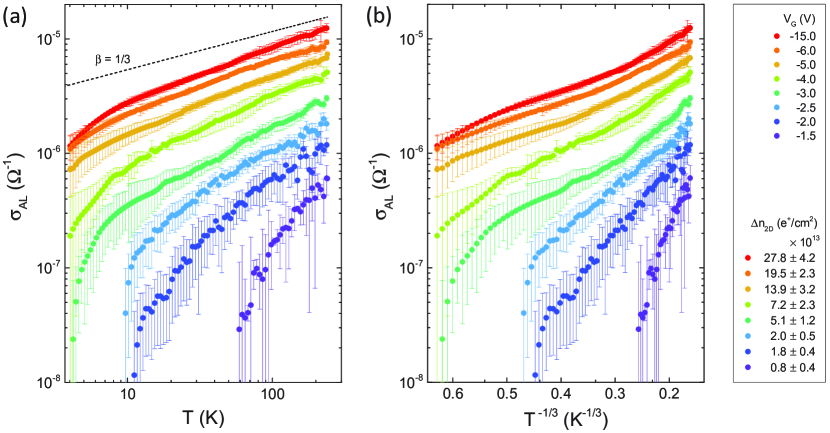
Since is small compared to , we measure both before and after each . For each value, we then calculate in the two cases and take their average, while their difference is taken as the uncertainty. Fig.3 shows the behavior of with increasing negative gate bias and surface carrier density .
It is immediately clear that not all the curves show the same scaling behavior with increasing . In panel a, is plotted in double logarithmic scale: For e+/cm2 (five uppermost curves) at any K, scales well as a power law:
| (2) |
As in the case of the bulk curves in Fig.2b, this scaling indicates that – although increases with – the gate-induced AL is not actually insulating. However, i) does not saturate below K, rapidly decreasing toward zero instead; and ii) its scaling exponent is always larger than . These findings indicate that the AL does not behave as a disordered metal either, and is instead in the QC regime slightly on the insulating side of the MIT McMillanPRB1981 ; LarkinJETP1982 ; HeegerPS2002 .
On the other hand, for e+/cm2 (three lowermost curves), decreases for decreasing faster than a power law in the entire range, indicating that the AL is outside the QC regime and charge transport occurs through a hopping mechanism between localized states HeegerPS2002 ; MottBook1979 ; MottBook1990 . This can be shown explicitly by plotting in semilogarithmic scale vs. , where can assume different values depending on the specific hopping process and the dimensionality of the system. As we show in Fig.3b, at low doping scales well with an exponent , the hallmark of Mott variable range hopping (VRH) in D HeegerPS2002 ; MottBook1979 ; MottBook1990 :
| (3) |
This behavior is reasonable, since the field-induced carriers are strongly confined at the surface in a quasi-2D hole system, and we don’t expect Coulomb interactions to play a strong role in this range of and doping BustarretPSS2008 . Indeed, does not show a good agreement with other values of , such as that of Mott VRH in D () or Efros-Shklovskii VRH in presence of a Coulomb gap ().
Our results show that employing B-doped diamond films increases the maximum achievable gate-induced surface carrier densities up to times with respect to undoped films as reported in the literature DankerlPRL2011 ; DankerlAPL2012 ; YamaguchiJPSJ2013 ; TakahidePRB2014 ; TakahidePRB2016 ; AkhgarNanoLett2016 . This likely stems from an increase in the EDL capacitance due to the sizable concentration of mobile carriers already at . Despite this advantage, the sheet conductance of the AL in our NCD films remains up to times smaller than the ones reported in undoped epitaxial films and single-crystals upon field-effect doping in the entire range YamaguchiJPSJ2013 ; TakahidePRB2014 ; TakahidePRB2016 ; AkhgarNanoLett2016 , and the AL is unable to cross to the metallic side of the MIT even for the largest values of . This can not be simply attributed to the presence of grain boundaries, since the bulk conductivity is firmly in the disordered metal regime. However, the gate-induced AL is confined within few atomic layers PiattiPRB2017 ; UmmarinoPRB2017 ; YeScience2015 ; SaitoScience2015 ; FeteAPL2016 ; PiattiApsusc2018 from a surface that features a much larger roughness nm, and local “valleys” between the grains (up to nm deep, see Fig.1a) may also lead to local percolative transport through the lighly-doped bulk. Therefore, disorder may be strongly amplified at the surface were the AL is confined, shifting the metallic edge of its MIT to much larger doping values with respect to the bulk.

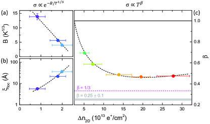
We can gain further insight into the surface transport close to the MIT by considering the dependence of the scaling factors in Eqs.2 and 3, and , with increasing hole density. In the VRH regime, strongly decreases at the increase of (see Fig.4a), and is related to the localization length as MottBook1979 ; MottBook1990 :
| (4) |
where is the Boltzmann constant, is the 2D-DOS at the Fermi level for parabolic bands, is the effective mass and is the reduced Planck constant. We determine (see Fig.4b) by assuming , where is the electron mass, which has been found to describe the DOS of diamond with a good degree of approximation IoffeInstDiam ; CollinsJPC1971 ; ProsserCJP1964 . As expected BustarretPSS2008 , is comparable with the Bohr radius of B-doped diamond ( Å) at low doping, and strongly increases as the AL approaches the MIT, where it would then diverge BustarretPSS2008 . If we perform a linear extrapolation of to e+/cm2, we find nm, comparable with the surface roughness . Therefore, the crossover from the VRH to the QC regime occurs when approaches the length scale describing the non-ideality of the surface.
In the QC regime, the behavior of the AL is described by the scaling factor . Theory predicts McMillanPRB1981 ; LarkinJETP1982 ; HeegerPS2002 that marks the transition from the VRH to the QC regime, the insulating side of the QC regime, and its metallic side. is exactly equal to only at the QC point of the MIT, where Eq.2 holds down to and the Fermi level is exactly at the mobility edge. In Fig.4c, we show that the AL sits firmly in the insulating side of the QC regime for any value of . As increases, first decreases and then saturates around for e+/cm2: the AL is unable to reach the QC point (dashed magenta line) and cross into the disordered metal regime of the underlying bulk (shaded grey area). We ascribe this behavior to extra scattering centers introduced by the ions in the EDL at the solid/electrolyte interface BragaNanoLett2012 ; SaitoACSNano2015 ; PiattiApsusc2017 ; Gonnelli2DMater2017 ; PiattiAPL2017 , an effect that can even lead to re-entrant MITs in extremely surface-sensitive materials OvchinnikovNatCommun2016 ; LuPNAS2017 . The gate-induced disorder shifts the Anderson transition to larger doping levels, eventually compensating the concomitant increase in and locking the AL in the QC regime on the insulating side of the MIT.
In summary, we have performed ionic gating experiments on nanocrystalline B-doped diamond films. We have shown that the presence of B doping enhances the maximum induced carrier density with respect to undoped films and single crystals. However, no sign of SC was observed down to K. By disentangling the sheet conductance of the field-induced accumulation layer from that of the underlying bulk, we were able to probe the surface transport properties as a function of temperature and induced charge density. By increasing the hole density, we observed a transition from the variable-range hopping to the quantum critical regime in the accumulation layer. Finally, we showed that the insulator-to-metal transition is never reached at the surface, and suggested that this frustrated behavior may be due to an increased disorder arising from a combination of non-negligible surface roughness and extra scattering centers introduced by the ionic gate.
Acknowledgments
We are very thankful to D. Romanin for theoretical and experimental support, to C. Gerbaldi and J. R. Nair for the design and preparation of the electrolytes, and to P. Olivero and F. Laviano for scientific support. G.P.’s work at Ulm University was supported by the Erasmus Traineeship programme of the European Union.
Author contributions
R.S.G. and E.P. designed the experiments. E.P. and F.G. realized the EDLT devices, performed the transport measurements and analyzed the data. G.P. and A.P. grew the samples. R.S.G. performed the AFM measurements and supervised both the experiments and the data analysis. E.P., F.G. and R.S.G. wrote the manuscript with input from all authors.
References
- (1) L. S. Pan and D. R. Kania, Diamond: Electronic Properties and Applications (Kluwer Academic Publishers, 1995)
- (2) E. A. Ekimov et al., Nature 428, 542 (2004)
- (3) E. Bustarret, Phys. Status Solidi A 205, 997 (2008)
- (4) Y. Takano et al., Appl. Phys. Lett. 85, 2851 (2004)
- (5) H. Okazaki et al., Appl. Phys. Lett. 106, 052601 (2015)
- (6) L. Boeri, J. Kortus, and O. K. Andersen, Phys. Rev. Lett. 93, 237002 (2004)
- (7) K.-W. Lee and W. E. Pickett, Phys. Rev. Lett. 93, 237003 (2004)
- (8) L. Boeri, J. Kortus, and O. K. Andersen, J. Phys. Chem. Solids 67, 552 (2006)
- (9) F. Giustino et al., Phys. Rev. Lett. 98, 047005 (2007)
- (10) K. Nakamura et al., Phys. Rev. B 87, 214506 (2013)
- (11) K. Ueno et al., J. Phys. Soc. Jpn. 83, 032001 (2014)
- (12) M. Dankerl et al., Phys. Rev. Lett 106, 196103 (2011)
- (13) M. Dankerl et al., Appl. Phys. Lett. 100, 023510 (2012)
- (14) T. Yamaguchi et al., J. Phys. Soc. Jpn. 82, 074718 (2013)
- (15) Y. Takahide et al., Phys. Rev. B 89, 235304 (2014)
- (16) Y. Takahide et al., Phys. Rev. B 94, 161301(R) (2016)
- (17) G. Akhgar et al., Nano Lett. 16, 3768 (2016)
- (18) D. Daghero et al., Phys. Rev. Lett. 108, 066807 (2012)
- (19) M. Tortello et al., Appl. Surf. Sci. 269 17 (2013)
- (20) E. Piatti et al., Phys. Rev. B 95, 140501(R) (2017)
- (21) G. A. Ummarino et al., Phys. Rev. B 96, 064509 (2017)
- (22) E. Piatti et al., Phys. Rev. Materials 3, 044801 (2019)
- (23) R. S. Gonnelli et al., Sci. Rep. 5, 9554 (2015)
- (24) E. Piatti et al., J. Supercond. Nov. Magn. 29, 587 (2016)
- (25) L. J. Li et al., Nature 529, 185 (2016)
- (26) G. Pippione et al., Phys. Status Solidi A 214, 1700223 (2017)
- (27) K. Ushizawa et al., Diam. Relat. Mater. 7, 1719 (1998)
- (28) G. Inzelt, in Electroanalytical Methods: Guide to Experiments and Applications, edited by F. Scholz (Springer-Verlag, Berlin, 2010), p. 147-158
- (29) W. L. McMillan, Phys. Rev. B 24, 2739 (1981)
- (30) A. I. Larkin and D. E. Khmel’nitskii, J. Exp. Theor. Phys. 56, 647 (1982)
- (31) A. J. Heeger, Phys. Scr. 2002, 30 (2002)
- (32) P. Gonon et al., J. Appl. Phys. 78, 7059 (1995)
- (33) S. Kouno et al., Sci Rep. 8, 14731 (2018)
- (34) N. F. Mott and E. A. Davis, Electronic Processes in Noncrystalline Materials (Oxford University Press, Oxford, 1979)
- (35) N. F. Mott, Metal-Insulator Transition (Taylor & Francis, London, 1990)
- (36) J. M. Lu et al., Science 350, 1353 (2015)
- (37) Y. Saito, Y. Kasahara, J. T. Ye, Y. Iwasa, and T. Nojima, Science 350, 409 (2015)
- (38) A. Fête, L. Rossi, A. Augieri, and C. Senatore, Appl. Phys. Lett. 109, 192601 (2016)
- (39) E. Piatti et al., Appl. Surf. Sci 461, 17 (2018)
- (40) http://www.ioffe.ru/SVA/NSM/Semicond/Diamond/ bandstr.html#masses
- (41) A. T. Collins and A. W. S. Williams, J. Phys. C.: Solid State Phys. 4, 1789 (1971)
- (42) V. Prosser, Czech. J. Phys. B15, 128 (1964)
- (43) D. Braga et al., Nano Lett. 12, 5218 (2012)
- (44) Y. Saito and Y. Iwasa, ACS Nano 9, 3192 (2015)
- (45) E. Piatti et al., Appl. Surf. Sci. 395, 37 (2017)
- (46) R. S. Gonnelli et al., 2D Mater. 4, 035006 (2017)
- (47) E. Piatti, Q. H. Chen, and J. T. Ye, Appl. Phys. Lett. 111, 013106 (2017)
- (48) D. Ovchinnikov et al., Nat. Commun. 7, 12391 (2016)
- (49) J. M. Lu et al., Proc. Nat. Acad. Sci. USA 115, 3551 (2018)