Wigner solid pinning modes tuned by fractional quantum Hall states of a nearby layer
We study a bilayer system hosting exotic many-body states of two-dimensional electron systems (2DESs) in close proximity but isolated from one another by a thin barrier. One 2DES has low electron density and forms a Wigner solid (WS) at high magnetic fields. The other has much higher density and, in the same field exhibits fractional quantum Hall states (FQHSs). The WS manifests microwave resonances which are understood as pinning modes, collective oscillations of the WS within the small but finite ubiquitous disorder. Our measurements reveal a striking evolution of the pinning mode frequencies of the WS layer with the formation of the FQHSs in the nearby layer, evincing a strong coupling between the WS pinning modes and the state of the 2DES in the adjacent layer, mediated by screening.
Introduction
Wigner solids occur when electron-electron interaction dominates the zero-point or thermal motion of the carriers. They can be accessed in extremely dilute systems in the absence of magnetic field or in high magnetic field () at sufficiently low Landau level filling, , at the termination of the FQHS series, where Wigner solids have long been expected (?, ?, ?). The magnetic-field-induced WS in a 2DES is of great interest and has been studied experimentally by a variety of different techniques including pinning mode spectroscopy (?, ?, ?, ?, ?, ?, ?), photoluminescence (?), transport (?, ?, ?, ?), NMR (?) and time-dependent tunneling (?). As a state stabilized by electron-electron interaction, it can be expected that a WS is strongly affected by nearby screening layers or its dielectric environment. There are theoretical works (?, ?), concerning the phase diagram of a 2DES in the presence of a nearby metal gate, for which the gate carries image charge that renders electron-electron interaction dipolar at distances exceeding the gate separation. For a WS near a higher-dielectric-constant substrate, the screening is less strong, and image charge magnitude is less than , as was studied (?, ?) for electrons separated from such substrates by thin He films.

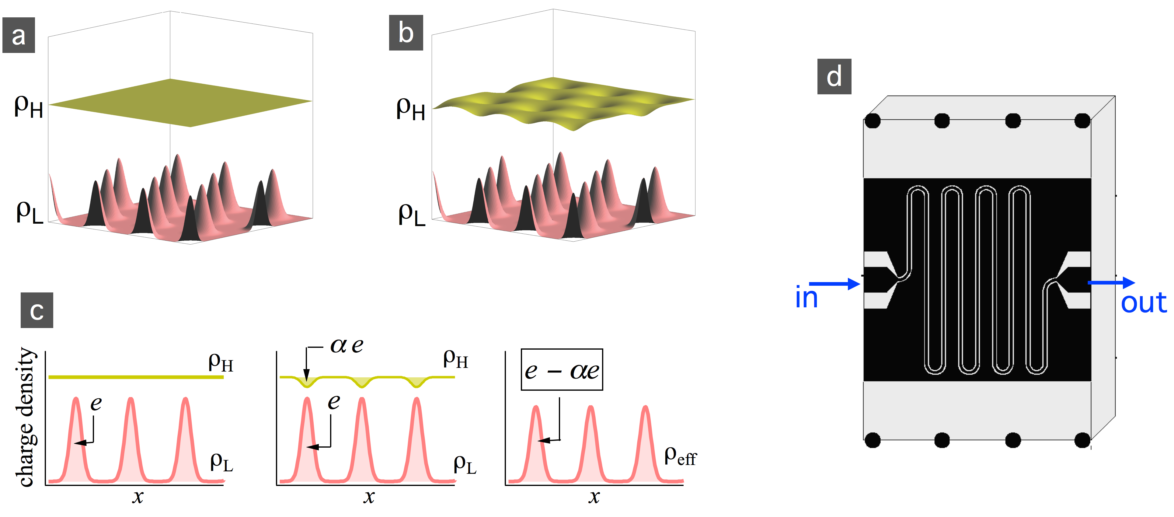
Through pinning mode measurements (?, ?, ?, ?, ?, ?, ?), we study here a 2D WS screened by a much larger density 2DES in a neighboring quantum well (QW). Previous dc-transport studies (?) of such density-asymmetric double wells have demonstrated the existence of a triangular-lattice WS in close proximity to a majority layer with a composite fermion (CF) (?) metal near , by means of geometric resonance oscillations of the CFs acted on by the WS. Our work considers the reverse, and examines the effect of the CF metal and nearby majority-layer FQHSs on the statics and pinning-mode dynamics of the WS. In agreement with Ref. (?) we find strong pinning modes signifying the presence of a WS. The frequencies of these modes exhibit a remarkable dependence on the FQHSs formed in the nearby majority layer, allowing us to extract unique and unexpected information regarding the screening of the WS by this layer. The screening is closest to the dielectric-substrate case rather than the metal-gate case, and can be modeled by image charges less than those at WS sites, as illustrated in Fig. 1.
Experimental Setup
Our samples contain two -nm-wide GaAs QWs separated by a -nm-thick, undoped barrier layer of Al0.24Ga0.76As, giving a center-to-center separation of nm. The QWs are modulation-doped with Si -layers asymmetrically: the bottom and top spacer layer thicknesses are nm and nm, respectively. This asymmetry leads to the different 2D electron densities in the QWs. As cooled, the densities of the top, high-density layer and the bottom, low-density layer are and , in units of cm-2, which will be used for brevity in the rest of the paper. A bottom gate is used to control . As detailed in the Supplement, we obtained and following the procedure of Deng et al. (?, ?), adapted for microwave conductivity measurements using the setup in Fig. 1(d). -dependent charge transfer between layers for samples like ours is possible, and occurs mainly for . To account for this, the total density (), which does not change with , is obtained from low- Shubnikov-de Haas oscillations, comes from high- majority-layer FQHS positions, and in the range of interest is found by taking the difference between and .


Results
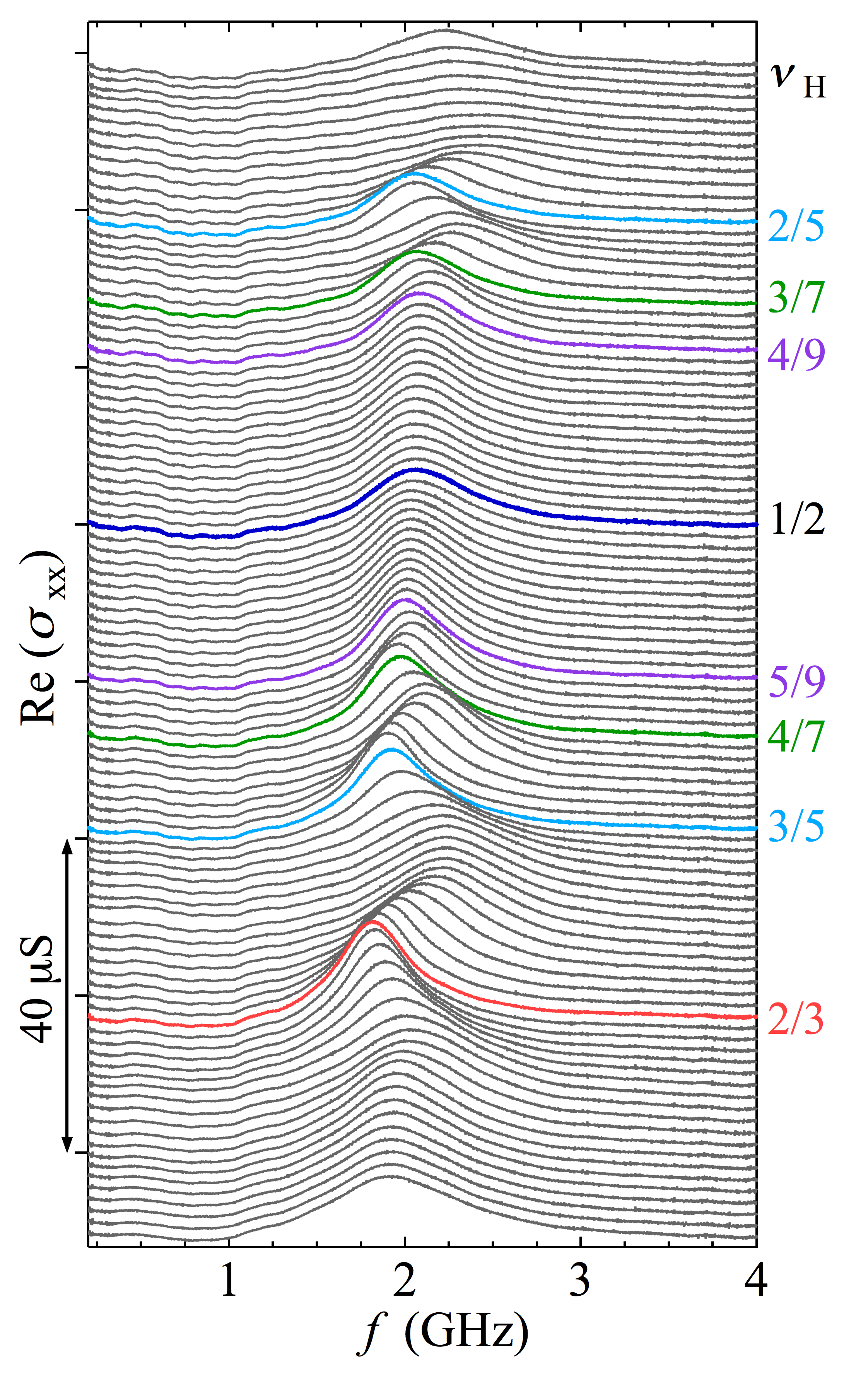
The main result of this paper is contained in Fig. 2, which shows pinning modes exhibited by the WS in the minority layer, as and hence the majority-layer filling, , are varied. The striking feature is that, although the WS resides in the minority layer, the pinning modes are clearly responding to the FQHSs of the majority layer, whose filling is marked at right in the figure. The effect of the majority-layer state on the pinning modes makes it clear that screening of the WS is present. Throughout the measurement range the minority layer filling , well within the filling-factor range of WS for high-quality, single-layer 2DESs (?, ?, ?, ?, ?).
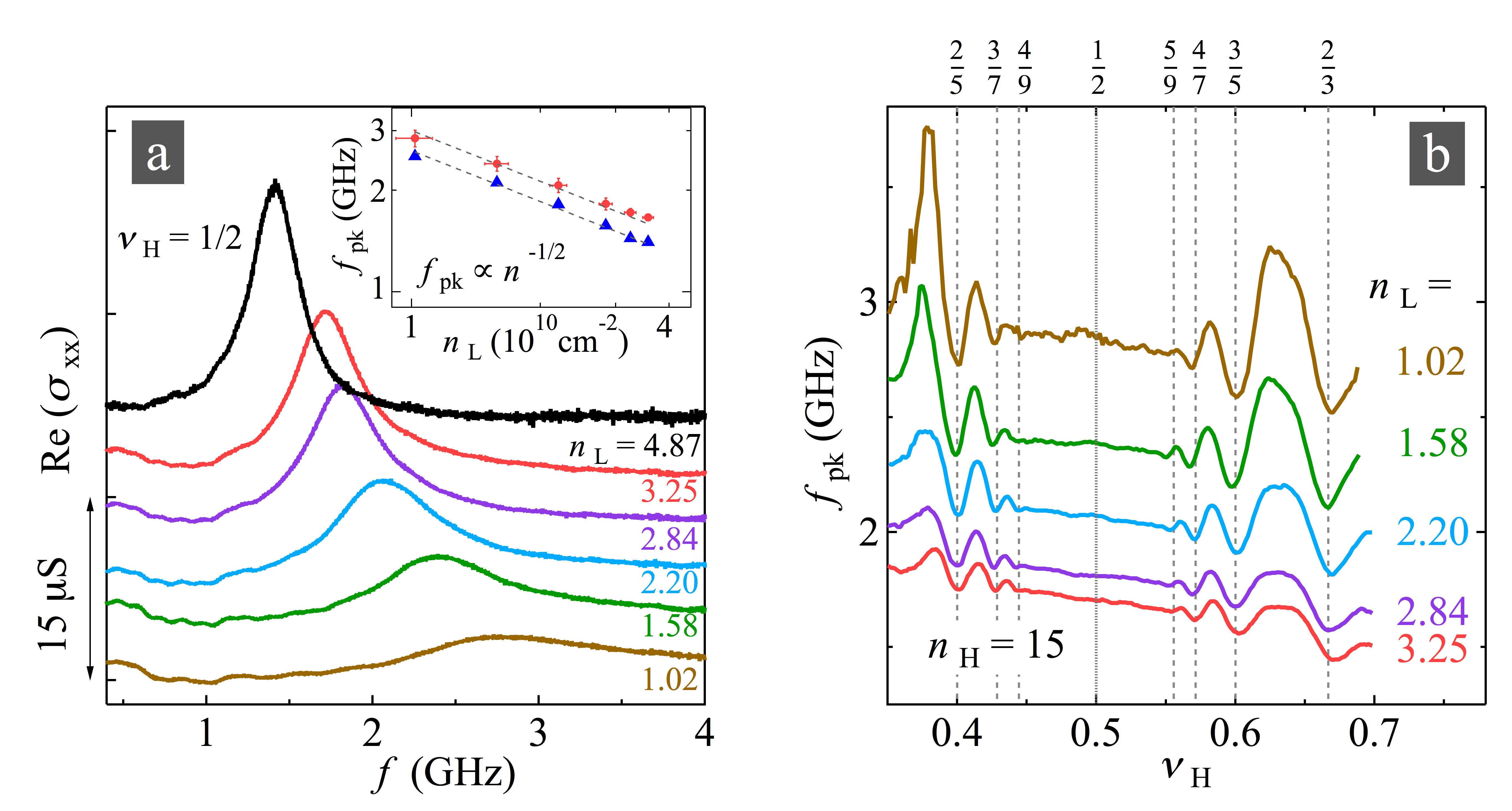
Figure 3(a) illustrates the effect of varying on the pinning mode of the minority layer. Re vs spectra are shown at different , produced by changing backgate voltage bias. Typical of pinning modes in a single-layer WS at low (?, ?, ?), when decreases, the peak frequency increases and the resonance becomes broader and weaker. We will refer to this behavior as the density effect. Its explanation in weak-pinning theory (?, ?, ?) is that, as the WS softens at lower density, the carrier positions become more closely associated with disorder, and so on average experience a larger restoring force due to a small displacement. The inset of Fig. 3(a) shows the extracted vs . The lines are fits to ; such a dependence has been observed previously (?, ?, ?) for single-layer samples at low densities in the low- WS range.
To highlight the clear response of the pinning mode to the majority-layer state, most strikingly the reduction of when a FQHS develops in the majority layer at its odd-denominator fillings and , in Fig. 3(b we show as a function of for various . As decreases, the overall curves shift upward over the entire range. The oscillation amplitudes of seen in Fig. 3(b) at FQHSs of the majority layer become more pronounced when decreases. This is occurring as the spacing of the minority-layer WS electrons exceeds the 40 nm interlayer separation of the double-QW structure. For example, at and , the triangular WS lattice constant is and nm, respectively.
The FQHS minima in Fig. 3(b) appear on top of a weak decreasing background: for each trace, the oscillations, and also its featureless region between and , are superimposed on a gradual decrease with . The decrease is similar for each trace, hence insensitive to . In light of this insensitivity, we ascribe the decreasing background to effects intrinsic to the minority layer. For example, such effects could be a change in the WS stiffness (?) or a change in the disorder coupling (?, ?, ?) due to a change in the magnetic length (size of the carrier). Single-layer WSs are known to show weak dependence of on over wide ranges of Landau filling (?).

Discussion
Our interpretation of the data relies on the picture of Fig. 1, in which, above the pinned WS lattice sites in the minority layer, the majority-layer local charge density develops “image” charge minima. The amount of charge in each image depends on the static dielectric response of the majority layer, not its conductivity. The ability of the image charge to follow the WS site charge dynamically as the pinning mode is driven, on the other hand, depends on the local conductivity of the majority layer as well. At each WS lattice site, there is then a combination of an image charge with the corresponding charge in the WS. This combined object has a dipole moment, but, because of the finite majority-layer local compressibility, it can also have a nonzero charge. We will characterize our pinning mode data in terms of charge densities. denotes the static charge density of the combined charges, and denotes the (dynamic) areal charge density that moves as the pinning mode is driven. Like , and are given in units of cm-2. A static polarizability, , as in the caption of Fig. 1, can be defined as .
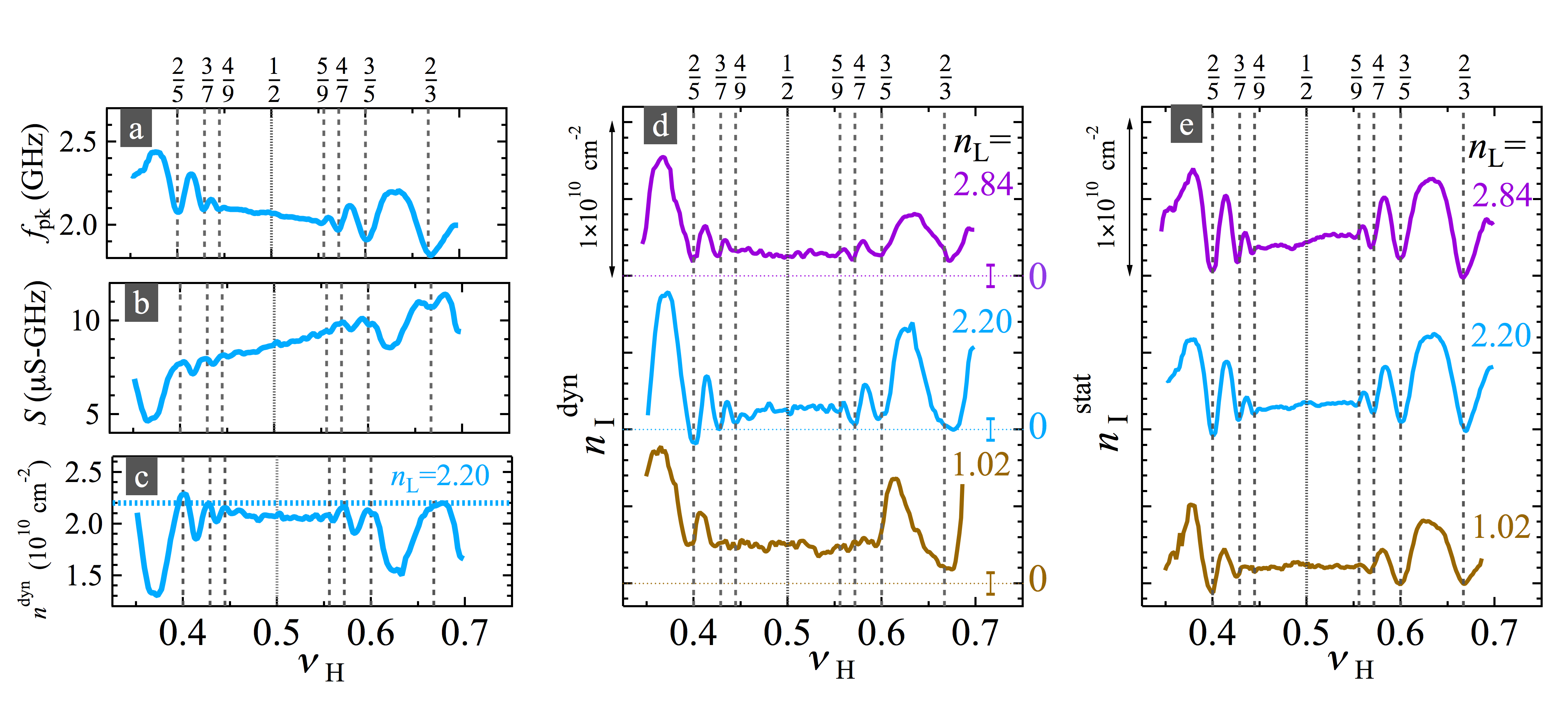
By means of the pinning mode sum rule (?), , where is the integrated Re vs frequency, , for the resonance. Figures 4(a-c) show, for , how is determined: vs in panel (a) and from panel (b) produce in panel (c) by use of the sum rule. tends to increase as decreases and vice versa. is increased near the majority-layer FQHS states, reflecting a lack of available cancelling image charge at these low-compressibility states. In panel (c), near the peaks at the most developed FQHSs ( and ), approaches , which is shown as a horizontal line. The difference of and is the image charge density in the majority layer that is moving along with the electrons of the WS, reducing the total current due to the resonance. We call the dynamic image charge density, . It is graphed vs for and in Fig. 4(d). shows minima at the majority-layer FQHSs, reflecting their small compressibility and small conductivity.
The static image charge density , obtained as , is of particular interest because of its sensitivity to the dielectric response of the majority layer without the influence of the conductivity. It is plotted in Fig. 4(e). While there is no direct method to measure or , we can estimate their variations as sweeps through the FQHSs of the majority layer. We obtain independently from , from the data of Fig. 3(b) alone. This is possible because in weak-pinning theories (?, ?, ?), is solely determined by the stiffness of the WS and the disorder acting on it. Increasing the density of a WS raises its stiffness. As described in the Supplement, the density-effect law, is inverted to find to within an additive constant. By obtaining from the density-effect law we are treating as if the image charge were on the same layer as the WS; because there is an interlayer separation on the order of the WS lattice constant, this will overestimate the effect of , so that the we obtain are lower-limit estimates of the true image charge.
A valid low estimate for the absolute at , is obtained by neglecting the finite compressibility of the majority layer at and taking . For the three values of Fig. 4, 1.02, 2.20 and 2.84, we find this low-estimate is about 10% of . The values of are on the order of their error, also about 10% of . Overall, we find the variations of and to be of similar size for most . This implies that the image charge in the majority layer moves with the WS as the resonance is driven.
In summary we study a WS separated from FQHSs by a distance comparable to its lattice constant. We observe a pinning mode from the minority-layer WS, indicating its existence even in the presence of the nearby, screening majority layer. The pinning mode is strongly affected by the majority-layer FQHSs, exhibiting a reduction in with an increase in around FQHEs. We find that these phenomena can be modeled by considering image charges in the majority layer, and regarding them as reducing the WS charge. The results indicate that in large part the image charge oscillates as the pinning mode is driven. The image charge is assessed to be about 10% of the WS charge near , but substantially larger elsewhere, particularly at the transitions between FQHSs.
Methods
We performed microwave spectroscopy (?, ?, ?, ?, ?) using a coplanar waveguide (CPW) patterned in Cr:Au film on the top surface of the sample. A top view schematic of the measurement is shown in Fig. 1 (d). We calculate the diagonal conductivity as , where m is the distance between the center conductor and ground plane, mm is the length of the CPW, is the characteristic impedance without the 2DES, is the transmitted signal amplitude and is the normalizing amplitude. The microwave measurements were carried out in the low-power limit, such that the results are not sensitive to the excitation power at our bath temperature of mK.
Acknowledgements
We thank Ju-Hyun Park and Glover Jones for their expert technical assistance, and J. P. Eisenstein for discussions. The microwave spectroscopy work at the National High Magnetic Field Laboratory (NHMFL) was supported through Department of Energy Basic Energy Sciences (DOE-BES) grant DE-FG02-05-ER46212 at NHMFL/FSU. The NHMFL is supported by National Science Foundation (NSF) Cooperative Agreement Nos. DMR-1157490 and DMR-1644779, by the State of Florida, and by the DOE. The work at Princeton University was funded by the Gordon and Betty Moore Foundation through the EPiQS initiative Grant GBMF4420, and by the DOE BES grant DE-FG02-00-ER45841 and the NSF through grant DMR-1709076 and MRSEC Grant DMR-1420541. Data displayed in this manuscript will be available by email request to engel@magnet.fsu.edu.
Contributions
A.T.H. conceived and designed the experiment, performed the microwave measurements, analyzed the data and co-wrote the manuscript. L.W.E. conceived and designed the experiment, discussed data analysis and co-wrote the manuscript. H.D., Y.L. and M. S. conceived the experiment, discussed data analysis and co-wrote the manuscript. L.N.P., K.W.W. and K.W.B. were responsible for the growth of the samples.
References
- 1. Y. E. Lozovik, V. Yudson, Crystallisation of a two dimenssional electron gas in magnetic field. JETP Letters 22, 11 (1975).
- 2. K. Yang, F. D. M. Haldane, E. H. Rezayi, Wigner crystals in the lowest landau level at low-filling factors. Phys. Rev. B 64, 081301 (2001).
- 3. J.-W. Rhim, J. K. Jain, K. Park, Analytical theory of strongly correlated Wigner crystals in the lowest landau level. Phys. Rev. B 92, 121103 (2015).
- 4. E. Y. Andrei, G. Deville, D. C. Glattli, F. I. B. Williams, E. Paris, B. Etienne, Observation of a magnetically induced Wigner solid. Phys. Rev. Lett. 60, 2765–2768 (1988).
- 5. F. I. B. Williams, P. A. Wright, R. G. Clark, E. Y. Andrei, G. Deville, D. C. Glattli, O. Probst, B. Etienne, C. Dorin, C. T. Foxon, J. J. Harris, Conduction threshold and pinning frequency of magnetically induced Wigner solid. Phys. Rev. Lett. 66, 3285–3288 (1991).
- 6. C.-C. Li, J. Yoon, L. W. Engel, D. Shahar, D. C. Tsui, M. Shayegan, Microwave resonance and weak pinning in two-dimensional hole systems at high magnetic fields. Phys. Rev. B 61, 10905–10909 (2000).
- 7. P. D. Ye, L. W. Engel, D. C. Tsui, R. M. Lewis, L. N. Pfeiffer, K. W. West, Correlation lengths of the Wigner-crystal order in a two-dimensional electron system at high magnetic fields. Phys. Rev. Lett. 89, 176802 (2002).
- 8. Y. P. Chen, R. M. Lewis, L. W. Engel, D. C. Tsui, P. D. Ye, Z. H. Wang, L. N. Pfeiffer, K. W. West, Evidence for two different solid phases of two-dimensional electrons in high magnetic fields. Phys. Rev. Lett. 93, 206805 (2004).
- 9. G. Sambandamurthy, Z. Wang, R. M. Lewis, Y. P. Chen, L. W. Engel, D. C. Tsui, L. N. Pfeiffer, K. W. West, Pinning mode resonances of new phases of 2d electron systems in high magnetic fields. Solid State Commun. 140, 100 - 106 (2006).
- 10. Z. Wang, Y. P. Chen, H. Zhu, L. W. Engel, D. C. Tsui, E. Tutuc, M. Shayegan, Unequal layer densities in bilayer Wigner crystal at high magnetic fields. Phys. Rev. B 85, 195408 (2012).
- 11. I. V. Kukushkin, V. I. Falko, R. J. Haug, K. von Klitzing, K. Eberl, K. Totemayer, Evidence of the triangular lattice of crystallized electrons from time resolved luminescence. Phys. Rev. Lett. 72, 3594-3597 (1994).
- 12. H. W. Jiang, R. L. Willett, H. L. Stormer, D. C. Tsui, L. N. Pfeiffer, K. W. West, Quantum liquid versus electron solid around Landau-level filling. Phys. Rev. Lett. 65, 633–636 (1990).
- 13. V. J. Goldman, M. Santos, M. Shayegan, J. E. Cunningham, Evidence for two-dimentional quantum Wigner crystal. Phys. Rev. Lett. 65, 2189–2192 (1990).
- 14. M. Shayegan, in Perspectives in Quantum Hall Effects, edited by S. Das Sarma and A. Pinczuk (Wiley-Interscience, New York, 1997), p. 343.
- 15. H. Deng, Y. Liu, I. Jo, L. N. Pfeiffer, K. W. West, K. W. Baldwin, M. Shayegan, Commensurability oscillations of composite fermions induced by the periodic potential of a Wigner crystal. Phys. Rev. Lett. 117, 096601 (2016).
- 16. L. Tiemann, T. D. Rhone, N. Shibata, K. Muraki, Nmr profiling of quantum electron solids in high magnetic fields. Nat. Phys. 10, 648-652 (2014).
- 17. J. Jang, B. M. Hunt, L. N. Pfeiffer, K. W. West, R. C. Ashoori, Sharp tunnelling resonance from the vibrations of an electronic Wigner crystal. Nature Physics 13, 340 EP - (2016).
- 18. F. M. Peeters, Two-dimensional Wigner crystal of electrons on a helium film: Static and dynamical properties. Phys. Rev. B 30, 159–165 (1984).
- 19. B. Spivak, S. A. Kivelson, Phases intermediate between a two-dimensional electron liquid and Wigner crystal. Phys. Rev. B 70, 155114 (2004).
- 20. G. Mistura, T. Günzler, S. Neser, P. Leiderer, Microwave study of screened two-dimensional electron crystals on helium films. Phys. Rev. B 56, 8360–8366 (1997).
- 21. J. K. Jain, Composite Fermions (Cambridge University Press, Cambridge, 2007).
- 22. H. Deng, Y. Liu, I. Jo, L. N. Pfeiffer, K. W. West, K. W. Baldwin, M. Shayegan, Interaction-induced interlayer charge transfer in the extreme quantum limit. Phys. Rev. B 96, 081102 (2017).
- 23. R. Chitra, T. Giamarchi, P. L. Doussal, Pinned Wigner crystals. Phys. Rev. B 65, 035312 (2001).
- 24. H. A. Fertig, Electromagnetic response of a pinned Wigner crystal. Phys. Rev. B 59, 2120 (1999).
- 25. M. M. Fogler, D. A. Huse, Dynamical response of a pinned two-dimensional Wigner crystal. Phys. Rev. B 62, 7553–7570 (2000).
- 26. H. Fukuyama, P. A. Lee, Pinning and conductivity of two-dimensional charge-density waves in magnetic fields. Phys. Rev. B 18, 6245 (1978).