Sensitive radio-frequency read-out of quantum dots using an ultra-low-noise SQUID amplifier
Abstract
Fault-tolerant spin-based quantum computers will require fast and accurate qubit readout. This can be achieved using radio-frequency reflectometry given sufficient sensitivity to the change in quantum capacitance associated with the qubit states. Here, we demonstrate a 23-fold improvement in capacitance sensitivity by supplementing a cryogenic semiconductor amplifier with a SQUID preamplifier. The SQUID amplifier operates at a frequency near 200 MHz and achieves a noise temperature below 600 mK when integrated into a reflectometry circuit, which is within a factor 120 of the quantum limit. It enables a record sensitivity to capacitance of . The setup is used to acquire charge stability diagrams of a gate-defined double quantum dot in a short time with a signal-to-noise ration of about 38 in of integration time.
I Introduction
Electron spins in semiconductors are among the most advanced qubit implementations, and are a potential basis of scalable quantum computers fabricated using industrial processes DiVincenzo and IBM (2000); Veldhorst et al. (2017); Vandersypen et al. (2017). A useful computer must correct the errors that inevitably arise during a calculation, which requires high single-shot qubit readout fidelity Fowler et al. (2012). The full surface code for error detection requires approximately half the physical qubits to be read out in every clock cycle of the computer Terhal (2015). Until recently, single-shot readout in spin qubit devices could only be achieved via spin-to-charge conversion, detected by a nearby single-electron transistor (SET) or quantum point contact (QPC) charge sensor Hanson et al. (2007); Barthel et al. (2009); Gaudreau et al. (2011); Veldhorst et al. (2015). However, the hardware is simpler and smaller if it uses dispersive readout, which exploits the difference in electrical polarizability between the singlet and triplet spin states in a double quantum dot Petta et al. (2005); Petersson et al. (2010); Gonzalez-Zalba et al. (2015); Crippa et al. (2019). The resulting capacitance difference between the two qubit states can be monitored via a radio-frequency (RF) resonator bonded to one of the quantum dot electrodes. Similar dispersive shifts also occur at charge transitions in the quantum dots, such that the reflected signal assists with tuning to the desired electron occupation Crippa et al. (2017); Volk et al. (2019); de Jong et al. (2019). Dispersive readout has the advantage that it does not require a separate charge sensor, but often the capacitance sensitivity is insufficient for single-shot qubit readout even in systems with a long spin decay time Jung et al. (2012); Ares et al. (2016); Colless et al. (2013); Hile et al. (2015); Betz et al. (2015); Ahmed et al. (2018); Higginbotham et al. (2014). Recently, there have been demonstrations of dispersive single-shot readout in double quantum dot based systems Pakkiam et al. (2018); West et al. (2019); Urdampilleta et al. (2019); Zheng et al. (2019); Connors et al. (2019), but higher sensitivities are still desirable for improved readout fidelity.
High sensitivity also makes it possibly to rapidly measure charge stability diagrams and therefore speeds up quantum dot tuning. For example, fast measurement has enabled video-mode tuning using an RF setup attached to one of the electrodes of a double quantum dot Stehlik et al. (2015). Auto-tuning techniques Lennon et al. (2019); Moon et al. (2020); van Esbroeck et al. (2020), which are often limited by measurement time, also benefit from increased measurement speed.
High-fidelity readout, whether dispersive or using a charge sensor, relies on low-noise amplifiers to attain good capacitance sensitivity. Radio-frequency experiments until now have used semiconductor amplifiers cooled to 4 K. Even lower noise can be achieved using amplifiers based on superconducting quantum interference devices (SQUIDs). At microwave frequencies, Josephson parametric amplifiers (JPAs) and travelling wave parametric amplifiers approach the quantum limit of sensitivity Castellanos-Beltran and Lehnert (2007); Yamamoto et al. (2008); Macklin et al. (2015). Such amplifiers allow rapid measurements of charge parity in a double quantum dot Stehlik et al. (2015). However, the JPAs previously used for quantum dot readout have a linear amplification range limited to an input power of Stehlik et al. (2015); Schaal et al. (2019), they require a circulator inside the cryostat and a dedicated pump oscillator, and they are not commercially available. Most JPAs are optimized for a microwave frequency range well above 1 GHz, although operation as low as has been demonstrated Vesterinen et al. (2017); Schaal et al. (2019). However, a lower frequency is desirable because the charge dipole in a singlet-triplet qubit only responds adiabatically to changes in the electric field if the interdot tunnel rate is much larger than the read-out frequency. If, on the other hand, the readout frequency approaches the inter-dot tunnel rate, the quantum capacitance is suppressed and read-out times increase Chorley et al. (2012). Increasing the tunnel rate leads to inelastic spin relaxation Johnson et al. (2005), and it is therefore usually limited to no more than a few GHz Petta et al. (2005); Laird et al. (2006).
Here we demonstrate a radio-frequency reflectometry circuit, operating at , that employs a SQUID as the primary amplifier Mück and McDermott (2010). We find an amplifier noise temperature below 600 mK. This enables the reflectometry circuit to detect a capacitance signal with a sensitivity better than 0.1 . Attaching the reflectometry circuit to the ohmic contact of a GaAs double quantum dot, we acquire a Coulomb stability diagram with a resolution of points within 20 ms. The measurement time to distinguish the two states of a singlet-triplet qubit using gate-based capacitance sensing is estimated to be well below one microsecond even at low excitation power. This time should be short enough for single-shot readout.
This paper is organized as follows. Section II describes the measurement setup and its principle of operation. In Section III we characterize the amplifier and show how to optimize its noise and gain by adjusting the control bias settings. In Section IV, we tune the resonant tank circuit used in the reflectometry setup, and measure the capacitance sensitivity using a variable capacitor (varactor). The setup used in Sections III-IV contains a single quantum dot device that serves as a realistic load on the tank circuit. In Section V, this device is replaced by a double quantum dot, and the reflectometry circuit is used to measure the stability diagram and to estimate the minimum acquisition time. Section VI summarizes and evaluates the potential for qubit readout. Further technical details and measurements of the single quantum dot appear in the Supplementary Information.
II Measurement Setup
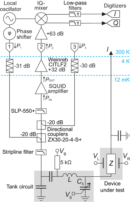
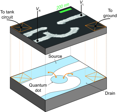
Figure 1 shows the reflectometry circuit used in the experiment. It is designed to sensitively measure two kinds of signal: changing capacitance in a varactor, and changing charge configuration in a laterally defined quantum dot. We have previously characterized these sensitivities using the same setup without the SQUID amplifier Ares et al. (2016). Quantum dots of the kind used in this experiment are defined in a GaAs/AlGaAs two-dimensional electron gas (2DEG) by applying depletion voltages to top gates. Here we use the device shown in Fig. 2, in which a quantum dot is defined by gate voltages and , and measured via source and drain contacts to the 2DEG. For the experiments of Sections III-IV this device was incorporated into the measurement circuit; however, in order to characterize the SQUID independently of the quantum dot, the dot was configured for very small conductance by applying large negative gate voltages and thereby also depleted of electrons.
The quantum dot device is wire-bonded to the RF circuit, that was assembled from chip components on a printed circuit board. The RF circuit includes a fixed inductor , a varactor of capacitance tuned by a voltage , and a terminal through which a DC source-drain bias voltage is applied to the quantum dot device (Fig. 1). These components form a resonant tank circuit with a total impedance that depends on the quantum dot impedance, the varactor tuning voltage, and the RF frequency. The circuit board is mounted in a 12 mK dilution refrigerator wired for reflectometry measurements. An RF input line (port 1) injects power into the tank circuit via a directional coupler. The reflected signal is passed to a SQUID amplifier at base temperature, boosted by a semiconductor postamplifier at 4 K, and then measured at port 2. Once this amplifier chain is configured appropriately, its noise is dominated by the SQUID amplifier, which therefore sets the measurement sensitivity Ares et al. (2016). A second RF input line (port 3), coupled via an oppositely oriented directional coupler, allows calibrated signals to be injected directly into the RF measurement line to characterize the amplifier chain independently of the resonant circuit. Both input lines contain attenuators to suppress thermal noise.
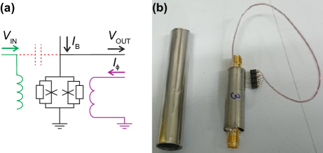
The SQUID amplifier is shown schematically in Fig. 3(a). It exploits the fact that the critical current of a DC SQUID depends on the instantaneous magnetic flux enclosed between the junctions. To operate the amplifier, an input signal is fed into a 20-turn superconducting coil, acting as an open-ended transmission line, through which it excites an oscillating magnetic field. The coil is fabricated over a Nb-based SQUID, separated by a 400 nm spacer layer, following the ‘washer’ geometry shown in Fig. 7(b) of Ref. Mück and McDermott (2010). The SQUID is biased with a current set greater than the maximum critical current. The resulting junction voltage depends on the instantaneous critical current, and its variation constitutes the amplifier’s output signal Mück and McDermott (2010). To optimize the gain, a flux offset is applied by means of a flux bias current applied to a nearby coil. The resonant frequency and quality factor of the input coil determine the optimum operating frequency and the bandwidth. The length of this input coil is chosen according to the desired operation frequency, since the gain peaks at a frequency that corresponds to approximately half a wavelength in the input coil Mück and McDermott (2010). The geometry was chosen to give an operating frequency near 200 MHz with a bandwidth around 60 MHz. Figure 3(b) shows a photograph of the amplifier with connectors. The picture also shows a shield, made of lead and Conetic QQ foil, into which the amplifier is inserted to suppress flux noise.
For frequency-domain experiments, the output at port 2 is measured directly using a spectrum analyzer or a network analyzer. For time-domain measurements, the signal is homodyne demodulated using a lock-in amplifier to yield in-phase and quadrature signals and , each filtered with time constant as in the circuit of Fig. 1.
III Characterizing and tuning the amplifier
We begin by characterizing the amplifier’s gain and noise. To achieve optimised signal-to-noise performance, we follow a tuning procedure that adjusts the current bias across the SQUID, the flux offset and input power. For the measurements in this section, the amplifier is driven by direct injection into port 3, and the output from port 2 is measured using a spectrum analyzer (see Fig. 1). The injected tone has a frequency , chosen for later compatibility with the tank circuit. For the measurements as a function of and , we set the power at port 3 to be , corresponding to a power at the SQUID input. The SQUID amplifier gain is determined by comparing the total transmission from port 3 to port 2 with the amplifier present, versus an identical measurement in which it is replaced by a short length of cable. The gain is:
| (1) |
where is the power at the amplifier output. The noise power is then determined by injecting a signal tone with power into the SQUID amplifier input, and measuring the output spectrum at port 2. The noise power referred to the amplifier input is then:
| (2) |
where is the power of the amplified signal tone and is the noise power, both measured at port 2. The system noise power can then be expressed as a noise temperature
| (3) |
where is the resolution bandwidth of the spectrum analyzer and is the noise temperature of the input signal into the SQUID amplifier. To accurately determine the power level , which depends on the transmission characteristics of the cables, we separately measured the attenuation of the injection path (see Supplementary Information). To avoid underestimating the system noise temperature, we assume the lowest possible electron temperature given perfect thermalization, i.e. . (In fact, our typical estimated electron temperature is mK Mavalankar2016 .) This assumption and the possibility of reflections on the amplifier input make an upper limit to the noise temperature of the SQUID amplifier.
Optimum operation, i.e. high amplifier gain and low noise, requires us to find suitable settings for both and . We follow a two-step process. First we increase until a change in is detected, indicating that the critical current has been exceeded. Next we optimize the flux offset via to find a steep point in the function , so that the output voltage is most sensitive to the induced flux.
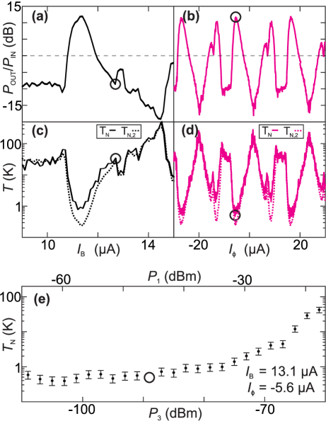
Figure 4 shows the performance of the amplifier as a function of the bias currents (Fig. 4(a),(c)) and (Fig. 4(b),(d)). At low , the SQUID is biased below its critical current and only a fraction of the input power is transmitted to the output by capacitive leakage. As is increased above the critical current a voltage develops and the gain increases abruptly. This occurs at in Fig. 4(a). At larger currents, the gain varies non-monotonically due to the self-inductance of the SQUID Clarke and Braginski (2005). These variations can be compensated by adjusting , and in fact we find that a similar gain can be achieved for all chosen values of larger than the critical current. Because the critical current depends on the flux, the chosen should be larger than the critical current for all .
We now measure the gain as a function of flux bias current (Fig. 4(b)). For this measurement, we choose (black marker in Fig. 4(a) and (c)). At first sight, Fig. 4(a) implies that is larger than optimal; the reason to choose this value is that on a previous cooldown, the critical current was as high as at (see Supplementary Information). By choosing above this value, we aim for it to be well above the critical current for all flux-offsets but not large enough to significantly heat the SQUID.
As shown in Fig. 4(b), the gain varies periodically with , reflecting the periodic dependence of critical current on flux. For an ideal SQUID at high current bias, the gain would be a sinusoidal function of flux. In fact, this amplifier has a more complex periodic dependence, which indicates that self-heating, junction asymmetry, and/or parasitic impedances play important roles in determining the gain Clarke and Braginski (2005). For example, junction asymmetry would unequally divide the bias current between the two arms of the SQUID, leading to a changing flux. To optimize the sensitivity we choose , (black marker in Fig. 4(b) and (d)), leading to a gain of dB. The uncertainty of this value is accumulated over multiple measurements that are needed to determine the losses of the insertion path and the gain of the postamplifier.
Figures 4(c) and 4(d) show the system noise temperature as a function of and of respectively. In both traces, the same bias settings that maximize the gain also lead to low noise. To distinguish the noise of the SQUID from the noise of the postamplifier, we plot as a dashed curve on the same axes the postamplifier’s contribution to the system noise temperature
| (4) |
where K is the input noise temperature of the postamplifier. This is the lowest noise temperature (referred to the SQUID input) that the system could achieve if the SQUID were a noiseless amplifier. Over most of the range, this contribution is approximately equal to the entire system noise (), meaning that the intrinsic noise of the SQUID is indeed undetectable. However, the optimal bias settings, with highest gain, lowest noise and therefore best signal-to-noise ratio, lead to , showing that for these settings the system noise is dominated by the SQUID contribution. Previous experiments have found this contribution to arise from hot electrons generated by ohmic dissipation Mück and McDermott (2010); Wellstood et al. (1994); Mück et al. (2001). There may also be a contribution from thermal radiation leaking into the SQUID. The lowest noise temperature observed is , obtained with (black marker in Fig. 4(d)). This is within a factor 120 of the quantum limit mK Clerk et al. (2010).
To study the amplifier dynamic range, Fig.(e) shows the noise temperature as a function of input power . The top axis shows an estimate of the corresponding power into port 1 that leads to the same power at the SQUID input when it is used for a reflectometry experiment (assuming that the matching circuit is optimized, as discussed below in Sec. IV.1 and Fig. 5). The noise increases at high input power, with the threshold being approximately , which corresponds to an amplifier input power of approximately . The input power corresponding to the onset of amplifier saturation can be roughly estimated from the SQUID parameters given by the manufacturer to be (see Supplementary). The lower dynamic range of the amplifier in our setup and the elevated noise temperature (compared to the state of the art in setups dedicated to optimised SQUID amplifier performance rather than sensitive RF read-out) could be related to poor input impedance matching between the SQUID and the components in the circuit, to radiation from outside the refrigerator, or to incomplete thermalization Mück and McDermott (2010).
IV Optimizing the capacitance sensitivity
We now show how to use the amplifier for sensitive measurements of capacitance. These measurements use a reflectometry configuration, in which the signal is injected via port 1 and the reflected signal is amplified by the SQUID. To avoid any contribution from the quantum capacitance, gate voltages are set to completely empty the quantum dot. To perform these measurements, we first tune the impedance of the tank circuit close to that of the measurement circuit, and then characterize the sensitivity to changes in the capacitance Ares et al. (2016).
The capacitance sensitivity is determined by modulating the varactor capacitance at a frequency while driving the tank circuit at carrier frequency .
The reflected signal, monitored at port 2 using a spectrum analyser, contains a main peak at and sidebands at . Such sidebands arise from mixing of an amplitude-modulated output signal when the impedance of the resonant circuit is sensitive to the modulated quantity. is extracted from the height of the sidebands above the noise floor (i.e. the signal-to-noise ratio or SNR, expressed in dB) according to Ares et al. (2016); Aassime et al. (2001); Brenning et al. (2006):
| (5) |
where is the spectrum resolution bandwidth and the root-mean-square modulation amplitude of the capacitance. To generate a capacitance modulation, we vary the control voltage of the varactor with amplitude , which is converted to the capacitance modulation as explained in the Supplementary Information.
IV.1 Optimizing the matching circuit
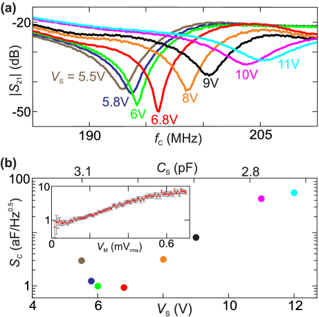
To optimize the impedance matching between the tank circuit and the input network, we tune the varactor using . Figure 5(a) shows the transmission from port 1 to port 2, which is proportional to the tank circuit’s reflection coefficient, for different settings of . The lowest reflection coefficient, and therefore the best match, is achieved at when .
Figure 5(b) shows the capacitance sensitivity as a function of measured with an input power of into port 1. This power corresponds to approximately on the SQUID input and is well below the threshold of amplifier saturation. The best sensitivity is . As expected, this occurs closest to perfect matching and therefore this varactor setting with the associated resonance frequency of is used in the remainder of Sec. IV Ares et al. (2016).
The inset of Fig. 5(b) is a plot of the sensitivity as a function of modulation amplitude , measured using the optimized matching parameters. These data show that the sensitivity degrades at high modulation amplitude due to non-linearity of the varactor, but confirm that the modulation applied in the main panel, , is within the linear range. In the following measurements (Sec. IV.2) we choose an even smaller modulation amplitude of .
IV.2 Optimizing the input power
Next we study how the capacitance sensitivity depends on the carrier power . Figure 6 shows that increasing improves the sensitivity, up to an optimal power of , where the sensitivity reaches . This power corresponds to approximately incident on the amplifier input, given the known losses due to attenuation and reflection on the tank circuit following the signal path associated with input port 1. From to around the sensitivity stays roughly constant before worsening at higher input powers.
We interpret these three regimes using the flux-to-voltage transfer function of the SQUID , as indicated by the insets in Fig. 6. For dBm, the amplifier is in its linear-response regime where the gain and the noise temperature are constant such that the sensitivity improves with increasing SNR at increasing input power. The region of approximately constant sensitivity between dBm and dBm indicates gain compression, which means that the flux induced by the input signal exceeds the linear range of . This creates harmonics sidebands in the output spectrum such that the SNR around the main sidebands decreases. For , when exceeds a quarter of a flux period, the amplifier reaches its saturation. At this point the flux oscillation reaches beyond the maxima and minima of and the sensitivity is degraded. The saturation threshold in Fig. 6 approximately matches the power threshold where begins to worsen (Fig. 4(e)). does not follow the noise temperature exactly because increasing the carrier power affects both the signal and the noise. In the next paragraph we will introduce a figure of merit that does not benefit from input power and follows the noise more closely.
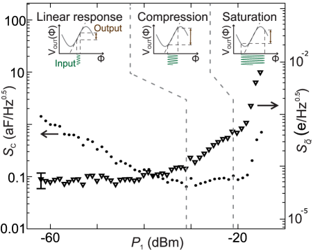
For dispersive readout of spin qubits, good capacitance sensitivity is not sufficient to achieve high fidelity. One reason is that it may require a large RF bias, giving rise to back action by exciting unwanted transitions in the qubit device. Another reason is that the quantum capacitance is usually sizable only within a small bias range, so that increasing the RF excitation improves without improving the qubit readout fidelity. This is the case for singlet-triplet qubits, where the quantum capacitance is large only near zero detuning Petersson et al. (2010). As explained in the Supplementary Information, for dispersive readout the crucial sensitivity is to the oscillating charge induced on the gate electrode by the qubit capacitance, which in our setup corresponds to the charge induced on one plate of the varactor. This sensitivity is
| (6) |
where is the root-mean-square RF voltage across the device Ares et al. (2016). This is a key figure of merit for dispersive spin qubit readout. For single-shot readout, this sensitivity must allow for detecting a charge smaller than one electron within the qubit lifetime. We estimate using a circuit model of the tank circuit as in Ref. Ares et al. (2016). For example, at , the incident power onto the tank circuit is , giving an estimated voltage across the device. The right axis of Fig. 6 shows as a function of input power into port 1. worsens at slightly lower input power than does , but reaches below for optimal settings.
V Fast readout of a double quantum dot
To demonstrate the full functionality of the circuit, we measure charge stability diagrams and determine the acquisition rate. We replace the single quantum dot from Fig. 1 with a double quantum dot operated in the Coulomb blockade regime Camenzind et al. (2019). For this experiment we use a different SQUID amplifier which includes a feedback capacitor between and , designed to lower its input impedance and thus improve the matching to the line impedance. We drive our circuit at with a power of , which is just below the threshold for broadening the Coulomb peaks in the double dot. To form the double dot, we automatically adjust the gate voltages with the help of machine-learning algorithm Moon et al. (2020).
The charge stability diagram of the double dot is shown in Fig. 7(a), which plots the normalised signal amplitude as a function of the left and right plunger voltages and . This plot shows the characteristic honeycomb pattern of a double quantum dot. In the centre of each honeycomb, Coulomb blockade suppresses conductance, and the reflected signal is large (red regions in Fig. 7 (a)); at the honeycomb boundaries, Coulomb blockade is partly lifted and the signal is small (blue regions in Fig. 7 (a)) Van der Wiel et al. (2002); Stehlik et al. (2015). As expected, the charge transitions of the left dot, closer to the RF electrode, give the strongest signal.
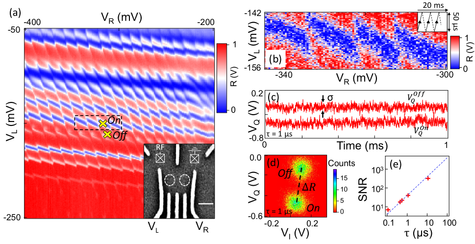
The low noise of the SQUID amplifier allows rapid measurement of the stability diagram. To show this, we focus on the region of the stability diagram marked by a dashed box in Fig. 7(a), and apply triangular waveforms via on-board bias tees to rapidly sweep and over this range. For these data, the filter time constant is set to . We record during the upward ramps of the fast triangular waveform in order to build up a two-dimensional map (Fig. 7(b)). The resolution is data points and the digitizer sample rate is , meaning that the entire plot is acquired within 20 ms. As expected, the resulting charge stability diagram, presented in Fig. 7(b), shows the same pattern as in Fig. 7(a), with easily distinguishable charge transitions despite the very short acquisition time.
The SNR can now be extracted directly by comparing a signal amplitude to the noise recorded in a time trace. The signal in this case is taken as the difference in reflected power between gate configurations on and off a Coulomb peak. To measure the SNR in Fig. 7(e) we record samples of and , digitized at a rate of , at two locations in the charge stability diagram in Fig. 7(a); and at location marked by On and and at location marked by Off. This experiment is repeated for different choices of filter time constant . A typical pair of time traces is shown in Fig. 7(c). Figure 7(d) represents these data as a joint histogram in the quadrature space. The two well-separated Gaussian distributions show that the two Coulomb states can be distinguished within a single time interval of duration s. The amplitude of the signal is defined as the distance between the mean values of the two distributions and the noise is their standard deviation (which as expected is the same in both and channels). The signal-to-noise ratio is plotted as function of in Fig. 7(e). The blue dashed line is a fit according to
| (7) |
with fit parameter , which is the extrapolated time to distinguish the two configurations with SNR of unity. The point at falls slightly above the fit line because the integration time of the digital converter () adds extra averaging. From these data, the sensitivity to a quasi-static charge of the double-dot device is at least as good as
| (8) |
In this expression, is the difference in charge induced on the quantum dot between the two measured configurations, which is a large fraction of one electron charge.
In the Supplementary Information we present a measurement of the sensitivity to a small charge modulation , measured on the steep flank of a Coulomb peak using a single-dot device. This leads to a somewhat better sensitivity, but is not directly comparable because it was measured using a different amplifier. Both these charge sensitivities are distinct from the sensitivity plotted in Fig. 4; is a charge oscillating in response to the RF field, whereas and are quasistatic charges. The former is what is measured in a dispersive measurement, the latter are what is measured using a charge sensor.
VI Discussion
We have shown that radio-frequency measurements using a SQUID amplifier can attain much better sensitivity than using a cryogenic semiconductor amplifier alone. This advantage holds when the signal level is limited by the need to avoid back-action on the device being measured, which is nearly always the case for quantum devices. The SQUID measured here has a gain around 12 dB and reaches a noise temperature below 600 mK, which is approximately 7 times better than the (already optimized) semiconductor amplifier. When used to measure capacitance via radio-frequency reflectometry, it allows a record capacitance sensitivity of , which corresponds to an improvement by a factor of 23 compared with the same setup without the SQUID Ares et al. (2016). This setup can also be used with a single quantum dot charge sensor. In the Supplementary Information, we perform this measurement and find a charge sensitivity of , corresponding to an improvement by a factor of 27 compared to the setup without the SQUID Ares et al. (2016). This improvement is better than expected from the improved noise temperature alone, and probably also arises from lower cable loss and a different impedance matching condition to the amplifier input.
To put these results in the context of spin qubit readout, we estimate the dispersive read-out time in a singlet-triplet qubit with the RF circuit connected to a plunger gate. In this case, a difference in capacitance on the order of 2 fF needs to be resolved to determine the state of the qubit Petersson et al. (2010). Based on the capacitance sensitivity obtained in section IV we estimate a single-shot readout time of with our circuit (see Supplementary Information). Integrating a SQUID amplifier into a spin qubit setup should therefore significantly reduce the measurement noise, ultimately improving single-shot readout fidelity. This represents a major advantage for scalable quantum information processing architectures containing many qubits in a small space Veldhorst et al. (2017); Vandersypen et al. (2017).
As well as for qubit readout, this setup can also increase the sensitivity of other radio-frequency measurements. The fast measurements of a double quantum dot presented above demonstrate a minimum per-pixel integration time . This integration time is of the same order as the integration times in double-quantum dot measurements using Josephson parametric amplifiers Stehlik et al. (2015); Schaal et al. (2019) or high quality-factor microwave resonators Zheng et al. (2019), but was enabled by a commercially available amplifier without the need for a dedicated fabrication environment. In another application of our circuit, the improved sensitivity provided by the SQUID has enabled time-resolved measurements of a vibrating carbon nanotube transistor Wen et al. (2019).
Supplementary Material
See supplementary material for more explanation of the charge sensitivity, charge sensing measurements on a single quantum dot, data from a separate cool-down of the amplifier, details of the measurement calibration, and full instructions for installing and tuning the amplifier.
Acknowledgements
The work was funded by DSTL (contract 1415Nat-PhD_59), EPSRC (EP/J015067/1, EP/N014995/1), the Royal Academy of Engineering, a Marie Curie Fellowship, Templeton World Charity Foundation, and the the European Research Council (grant agreement 818751). We thank M. Mück and ez SQUID for supplying and assisting with the amplifiers.
The data that support the findings of this study are available from the corresponding author upon reasonable request.
References
- DiVincenzo and IBM (2000) D. P. DiVincenzo and IBM, Fortschritte der Physik: Progress of Physics 48, 771 (2000).
- Veldhorst et al. (2017) M. Veldhorst, H. G. J. Eenink, C. H. Yang, and A. S. Dzurak, Nature Communications 8, 1766 (2017).
- Vandersypen et al. (2017) L. M. K. Vandersypen, H. Bluhm, J. S. Clarke, A. S. Dzurak, R. Ishihara, A. Morello, D. J. Reilly, L. R. Schreiber, and M. Veldhorst, npj Quantum Information 3, 34 (2017).
- Fowler et al. (2012) A. G. Fowler, M. Mariantoni, J. M. Martinis, and A. N. Cleland, Physical Review A 86, 032324 (2012).
- Terhal (2015) B. M. Terhal, Reviews of Modern Physics 87, 307 (2015).
- Hanson et al. (2007) R. Hanson, L. P. Kouwenhoven, J. R. Petta, S. Tarucha, and L. M. K. Vandersypen, Reviews of Modern Physics 79, 1217 (2007).
- Barthel et al. (2009) C. Barthel, D. J. Reilly, C. M. Marcus, M. P. Hanson, and A. C. Gossard, Physical Review Letters 103, 160503 (2009).
- Gaudreau et al. (2011) L. Gaudreau, G. Granger, A. Kam, G. C. Aers, S. A. Studenikin, P. Zawadzki, M. Pioro-Ladrière, Z. R. Wasilewski, and A. S. Sachrajda, Nature Physics 8, 10 (2011).
- Veldhorst et al. (2015) M. Veldhorst, C. H. Yang, J. C. C. Hwang, W. Huang, J. P. Dehollain, J. T. Muhonen, S. Simmons, A. Laucht, F. E. Hudson, K. M. Itoh, A. Morello, and A. S. Dzurak, Nature 526, 410 (2015).
- Petta et al. (2005) J. R. Petta, A. C. Johnson, J. M. Taylor, E. A. Laird, A. Yacoby, M. D. Lukin, C. M. Marcus, M. P. Hanson, and A. C. Gossard, Science 309, 2180 (2005).
- Petersson et al. (2010) K. D. Petersson, C. G. Smith, D. Anderson, P. Atkinson, G. A. C. Jones, and D. A. Ritchie, Nano Letters 10, 2789 (2010).
- Gonzalez-Zalba et al. (2015) M. F. Gonzalez-Zalba, S. Barraud, A. J. Ferguson, and A. C. Betz, Nature Communications 2, 1 (2015).
- Crippa et al. (2019) A. Crippa, R. Ezzouch, A. Aprá, A. Amisse, R. Laviéville, L. Hutin, B. Bertrand, M. Vinet, M. Urdampilleta, T. Meunier, M. Sanquer, X. Jehl, R. Maurand, and S. De Franceschi, Nature Communications 10, 2776 (2019).
- Crippa et al. (2017) A. Crippa, R. Maurand, D. Kotekar-Patil, A. Corna, H. Bohuslavskyi, A. O. Orlov, P. Fay, R. Laviéville, S. Barraud, M. Vinet, et al., Nano Letters 17, 1001 (2017).
- Volk et al. (2019) C. Volk, A. Chatterjee, F. Ansaloni, C. M. Marcus, and F. Kuemmeth, Nano Letters 122, 5628 (2019).
- de Jong et al. (2019) D. de Jong, J. van Veen, L. Binci, A. Singh, P. Krogstrup, L. P. Kouwenhoven, W. Pfaff, and J. D. Watson, Physical Review Applied 11, 044061 (2019).
- Jung et al. (2012) M. Jung, M. D. Schroer, K. D. Petersson, and J. R. Petta, Applied Physics Letters 100, 253508 (2012).
- Ares et al. (2016) N. Ares, F. J. Schupp, A. Mavalankar, G. Rogers, J. Griffiths, G. A. C. Jones, I. Farrer, D. A. Ritchie, C. G. Smith, A. Cottet, G. A. D. Briggs, and E. A. Laird, Physical Review Applied 5, 034011 (2016).
- Colless et al. (2013) J. I. Colless, A. C. Mahoney, J. M. Hornibrook, A. C. Doherty, H. Lu, A. C. Gossard, and D. J Reilly, Physical Review Letters 110, 046805 (2013).
- Hile et al. (2015) S. J. Hile, M. G. House, E. Peretz, J. Verduijn, D. Widmann, T. Kobayashi, S. Rogge, and M. Y. Simmons, Applied Physics Letters 107, 093504 (2015).
- Betz et al. (2015) A. C. Betz, R. Wacquez, M. Vinet, X. Jehl, A. L. Saraiva, M. Sanquer, A. J. Ferguson, and M. F. Gonzalez-Zalba, Nano Letters 15 (7), 4622–4627 (2015).
- Ahmed et al. (2018) I. Ahmed, J. A. Haigh, S. Schaal, S. Barraud, Y. Zhu, C. M. Lee, M. Amado, J. W. A. Robinson, A. Rossi, J. J. L. Morton, and M. F. Gonzalez-Zalba, Physical Review Applied 10, 014018 (2018).
- Higginbotham et al. (2014) A. P. Higginbotham, T. W. Larsen, J. Yao, H. Yan, C. M. Lieber, C. M. Marcus, and F. Kuemmeth, Nano Letters 14, 3582 (2014).
- Pakkiam et al. (2018) P. Pakkiam, A. V. Timofeev, M. G. House, M. R. Hogg, T. Kobayashi, M. Koch, S. Rogge, and M. Y. Simmons, Physical Review X , 041032 (2018).
- West et al. (2019) A. West, B. Hensen, A. Jouan, T. Tanttu, C.-H. Yang, A. Rossi, M. F. Gonzalez-Zalba, F. Hudson, A. Morello, D. J. Reilly, Nature Nanotechnology 14, 437 (2019).
- Urdampilleta et al. (2019) M. Urdampilleta, D. J. Niegemann, E. Chanrion, B. Jadot, C. Spence, P.-A. Mortemousque, L. Hutin, B. Bertrand, S. Barraud, R. Maurand, M. Sanquer, X. Jehl, S. De Franceschi, M. Vinet, and T. Meunier, Nature Nanotechnology 14, 737 (2019).
- Zheng et al. (2019) G. Zheng, N. Samkharadze, M. L. Noordam, N. Kalhor, D. Brousse, A. Sammak, G. Scappucci, and L. M. Vandersypen, Nature Nanotechnology 14, 742 (2019).
- Connors et al. (2019) E. J. Connors, J. J. Nelson, and J. M. Nichol, Physical Review Applied 13, 024019 (2020).
- Stehlik et al. (2015) J. Stehlik, Y. Y. Liu, C. M. Quintana, C. Eichler, T. R. Hartke, and J. R. Petta, Physical Review Applied 4, 1 (2015).
- Lennon et al. (2019) D. Lennon, H. Moon, L. C. Camenzind, L. Yu, D. M. Zumbühl, G. A. D. Briggs, M. A. Osborne, E. A. Laird, and N. Ares, npj Quantum Information 5, 1 (2019).
- Moon et al. (2020) H. Moon, D. T. Lennon, J. Kirkpatrick, N. M. van Esbroeck, L. C. Camenzind, L. Yu, F. Vigneau, D. M. Zumbühl, G. A. D. Briggs, M. A. Osborne, D. Sejdinovic, E. A. Laird, and N. Ares, arXiv preprint arXiv:2001.02589 (2020).
- van Esbroeck et al. (2020) N. van Esbroeck, D. Lennon, H. Moon, V. Nguyen, F. Vigneau, L. C. Camenzind, L. Yu, D. M. Zumbühl, G. A. D. Briggs, D. Sejdinovic, and N. Ares, arXiv preprint arXiv:2001.04409 (2020).
- Castellanos-Beltran and Lehnert (2007) M. A. Castellanos-Beltran and K. W. Lehnert, Applied Physics Letters 91, 083509 (2007).
- Yamamoto et al. (2008) T. Yamamoto, K. Inomata, M. Watanabe, K. Matsuba, T. Miyazaki, W. D. Oliver, Y. Nakamura, and J. S. Tsai, Applied Physics Letters 93, 042510 (2008).
- Macklin et al. (2015) C. Macklin, K. O’Brien, D. Hover, M. E. Schwartz, V. Bolkhovsky, X. Zhang, W. D. Oliver, and I. Siddiqi, Science 350, 307 (2015).
- Schaal et al. (2019) S. Schaal, I. Ahmed, J. A. Haigh, L. Hutin, B. Bertrand, S. Barraud, M. Vinet, C.-M. Lee, N. Stelmashenko, J. W. A. Robinson, J. Y. Qiu, S. Hacohen-Gourgy, I. Siddiqi, M. F. Gonzalez-Zalba, and J. J. L. Morton, Physical Review Letters 124, 067701(2019).
- Vesterinen et al. (2017) V. Vesterinen, O.-p. Saira, I. Räisänen, M. Möttönen, L. Grönberg, J. Pekola, and J. Hassel, Superconductor Science and Technology 30, 085001 (2017).
- Chorley et al. (2012) S. J. Chorley, J. Wabnig, Z. V. Penfold-Fitch, K. D. Petersson, J. Frake, C. G. Smith, and M. R. Buitelaar, Physical Review Letters 108, 036802 (2012).
- Johnson et al. (2005) A. C. Johnson, J. R. Petta, J. M. Taylor, A. Yacoby, M. D. Lukin, C. M. Marcus, M. P. Hanson, and A. C. Gossard, Nature 435, 925 (2005).
- Laird et al. (2006) E. A. Laird, J. R. Petta, A. C. Johnson, C. M. Marcus, A. Yacoby, M. P. Hanson, and A. C. Gossard, Physical Review Letters 97, 056801 (2006).
- Mück and McDermott (2010) M. Mück and R. McDermott, Superconductor Science and Technology 23, 093001 (2010).
- (42) A. Mavalankar, S.J. Chorley, J. Griffiths, G. A. C. Jones, I. Farrer, D. A. Ritchie, C. G. Smith Applied Physics Letters 103, 133116 (2013).
- (43) A. Mavalankar, T. Pei, E. M. Gauger, J. H. Warner, G. A. D. Briggs, E. A. Laird Physical Review B 93, 235428 (2016).
- Clarke and Braginski (2005) J. Clarke and A. I. Braginski, in The SQUID Handbook (Wiley-VCH Verlag GmbH and Co. KGaA, Weinheim, FRG, 2005) pp. i–xvi.
- Wellstood et al. (1994) F. C. Wellstood, C. Urbina, and J. Clarke, Physical Review B 49, 5942 (1994).
- Mück et al. (2001) M. Mück, J. B. Kycia, and J. Clarke, Applied Physics Letters 78, 967 (2001).
- Clerk et al. (2010) A. A. Clerk, M. H. Devoret, S. M. Girvin, F. Marquardt, and R. J. Schoelkopf, Reviews of Modern Physics 82, 1155 (2010).
- Aassime et al. (2001) A. Aassime, G. Johansson, G. Wendin, R. J. Schoelkopf, and P. Delsing, Physical Review Letters 86, 3376 (2001).
- Brenning et al. (2006) H. Brenning, S. Kafanov, T. Duty, S. Kubatkin, and P. Delsing, Journal of Applied Physics 100 114321 (2006).
- Camenzind et al. (2019) L. C. Camenzind, L. Yu, P. Stano, J. D. Zimmerman, A. C. Gossard, D. Loss, and D. M. Zumbühl, Physical Review Letters 122, 207701 (2019).
- Van der Wiel et al. (2002) W. G. Van der Wiel, S. De Franceschi, J. M. Elzerman, T. Fujisawa, S. Tarucha, and L. P. Kouwenhoven, Reviews of Modern Physics 75, 1 (2002).
- Wen et al. (2019) Y. Wen, N. Ares, F. J. Schupp, T. Pei, G. A. D. Briggs, and E. A. Laird, Nature Physics 16, 75 (2019).