Defect energy levels and persistent luminescence in Cu-doped ZnS
Abstract
Zinc sulfide (ZnS) based materials are widely used in many applications. Yet, due to a lack of detailed knowledge of defect energy levels, the electrical properties and luminescence mechanisms in the materials still give rise to debate. Here, we report a first-principles study of native point defects and impurities in zincblende ZnS using hybrid density-functional calculations. We find that cation and anion vacancies and antisite defects introduce deep defect levels in the band gap and can act as donors or acceptors depending on the position of the Fermi level. The substitutional impurity CuZn acts as a deep acceptor and thus does not contribute to p-type conductivity. Substitutional impurities AlZn and ClS, on the other hand, are shallow donors. More importantly, we identify the isolated (i.e., unassociated) CuZn as a source of the green luminescence observed in ZnS-based phosphors and CuZn–AlZn and CuZn–ClS defect complexes as sources of blue luminescence. The materials may have both green and blue emissions with the relative intensity dependent on the ratio between the unassociated defect and defect complex concentrations, which is also consistent with experimental observations.
pacs:
I Introduction
ZnS has been of great interest for various applications, including display technologies, luminescent devices, and solar cells.Shionoya (2006); Xu et al. (2018) ZnS phosphors, for example, have a long history, dating back to the discovery of persistent luminescence in ZnS crystals by Théodore Sidot in 1866. It is now believed that copper impurities in Sidot’s crystals were responsible for the observed phenomenon.Shionoya (2006) ZnS-based phosphors can emit light in the blue, green, and red spectral regions, depending on the presence of certain native point defects and (intentional or otherwise) impurities. Although the materials have been widely used, the structure of defect centers and the associated luminescence mechanisms are still not well understood.
On the theory side, a number of first-principles studies of native defects and impurities–hereafter commonly referred to as defects–in zincblende (cubic) or wurtzite (hexagonal) ZnS have been reported;Li et al. (2012); Varley and Lordi (2013, 2014); Pham et al. (2015); Faghaninia et al. (2016) however, only limited information on Cu-related defects is available, especially in the case of the zincblende phase. Moreover, some of these studiesLi et al. (2012); Pham et al. (2015) are based on density-functional theory (DFT) within the local-density (LDA) or generalized gradient (GGA) approximationCeperley and Alder (1980); Perdew et al. (1992) and/or the DFT+ extensionAnisimov et al. (1991) where is the on-site Coulomb correction; these methods are known to have limited predictive power, often due to their inability to reproduce the experimental band gap and thus the position of defect levels in the band gap region. Yet an accurate determination of defect levels in the band gap caused by these defects is crucial to understanding the luminescence of Cu-doped ZnS materials.
Here, we report a first-principles study of defects and doping in zincblende ZnS using a hybrid DFT/Hartree-Fock approach.Perdew et al. (1996a) In addition to native point defects such as cation and anion vacancies, interstitials, and antisites, we consider substitutional Cu, Al, and Cl impurities and their complexes. Copper, aluminum, and clorine are chosen because they are often present in ZnS phosphors as dopants and/or unintentional impurities.Shionoya (2006); Bol et al. (2002); Corrado et al. (2009); Car et al. (2011) The focus of this work is on determining energy levels in the band gap region caused by the defects and identifying defect centers in Cu-doped ZnS phosphors that are responsible for the green and blue luminescence observed in experiments.
II Methods
Our calculations are based on DFT with the Heyd-Scuseria-Ernzerhof (HSE) hybrid functional,Heyd et al. (2003) as implemented in the Vienna Ab Initio Simulation Package (vasp).Kresse and Furthmüller (1996) The screening length is set to the default value of 10 Å, whereas the Hartree-Fock mixing parameter is set to 0.32 to match the experimental band gap. The Zn and S electrons are treated as valence electrons whereas the inner electrons as core states within the projector augmented wave method.Blöchl (1994) The plane-wave basis-set cutoff is 400 eV and spin polarization is included. In these calculations, the band gap () of zincblende ZnS is 3.66 eV, a direct gap at , almost identical to the experimental value (3.7 eV Shionoya (2006)). Defects are modeled using a 222 (64-atom) supercell and a 222 Monkhorst-Pack -point mesh for the integrations over the Brillouin zone. In the defect calculations, the lattice constant is fixed to the calculated bulk value (5.42 Å) but all the internal coordinates are relaxed (For comparison, the experimental lattice constant is 5.41 Å Shionoya (2006)). Note that spin-orbit coupling (SOC) is not included. We find that the electronic structure of ZnS obtained in HSE is almost identical to that obtained in HSESOC (see Fig. S1 in the Supplementary Material); the inclusion of SOC would thus have negligible effects on the energetics of the defects in ZnS. Besides, there is often strong cancellation between different terms in the defect formation energy.
A general native defect, impurity, or defect complex X in charge state (with respect to the host lattice) is characterized by its formation energy, defined asFreysoldt et al. (2014)
| (1) | |||||
where and are the total energies of a supercell containing the defect and the defect-free supercell. is the atomic chemical potential, accounting for the species either added () or removed () from the supercell to form the defect and representing the chemical reservoir with which the species is exchanged. is the electronic chemical potential, i.e., the Fermi level, which is the energy of the reservoir for electron exchange and, as a convention, referenced to the valence-band maximum (VBM) of the host (). Finally, is a correction term to align the electrostatic potentials of the bulk and defect supercells and to account for finite-size effects on the total energies of systems with charged defects.Freysoldt et al. (2009)
The chemical potentials of Zn and S are referenced to the total energy per atom of bulk Zn and S, respectively, and vary over a range determined by the calculated formation enthalpy of ZnS: eV. The extreme Zn-rich and S-rich conditions correspond to eV and eV, respectively. The chemical potentials of Cu, Al, and Cl are assumed to be limited by the formation of bulk Cu (or CuS) under the Zn-rich (S-rich) condition, Al2ZnS4, and ZnCl2, respectively. These assumptions result in eV ( eV), eV ( eV), and eV ( eV) under the Zn-rich (S-rich) condition. One, of course, can choose a different set of assumptions which correspond to different experimental conditions. It is noted, however, that our conclusions are not affected by the choice we made here as defect transition levels (see below) are independent of the atomic chemical potentials.
In the calculation of , a total static dielectric constant of 8.18 is used. This dielectric constant is calculated as the sum of the electronic contribution (4.67, obtained in calculations using the HSE functional) and the ionic contribution (3.51, obtained with the Perdew, Burke and Ernzerhof versionPerdew et al. (1996b) of GGA). For comparison, the experimental dielectric constant is reported to be 8.3.Shionoya (2006)
From defect formation energies, one can calculate the thermodynamic transition level between charge states and of a defect, , defined as the Fermi-level position at which the formation energy of the defect in charge state is equal to that in charge state , i.e,Freysoldt et al. (2014)
| (2) |
where is the formation energy of the defect X in charge state when the Fermi level is at the VBM (). This level would be observed in experiments where the defect in the final charge state fully relaxes to its equilibrium configuration after the transition. The optical transition level is defined similarly but with the total energy of the final state calculated using the atomic configuration of the initial state . Clearly, both the thermodynamic and optical transition levels are independent of the choice of the atomic chemical potentials.
III Results and Discussion
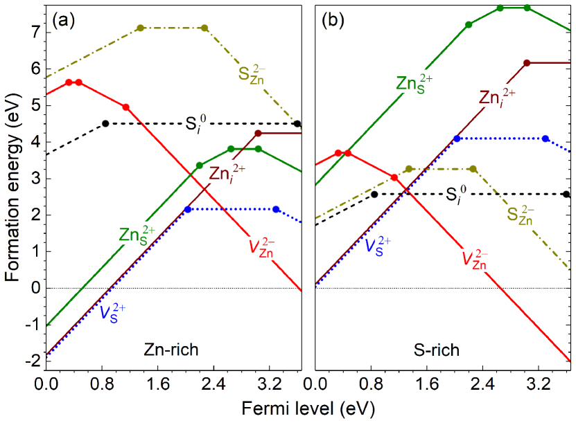
We begin with an examination of native point defects in zincblende ZnS. Figure 1 shows their calculated formation energies. In general, these defects (except the zinc interstitial, Zni) are amphoteric, acting as donors or acceptors depending on the position of the Fermi level. The sulfur vacancy, , is a deep donor with the transition level from the to charge states, , at 2.03 eV above the VBM. It can also behave as an acceptor under n-type conditions; the level is at 0.37 eV below the conduction-band minimum (CBM). In the defect configuration, the electron is delocalized over the four nearest Zn neighbors. The zinc vacancy, , on the other hand, behaves as a deep acceptor; the level is at 1.14 eV above the VBM and the level is at 0.47 eV. The defect can also act as a donor in the range of Fermi-level values closer to the VBM where it can be stable as ; the level is at 0.33 eV above the VBM. In the configuration, the electron hole is delocalized over the four nearest S neighbors. Similarly, antisite defects SZn and ZnS behave as deep donors (acceptors) for Fermi-level values closer to the VBM (CBM). SZn introduces energy levels at 1.35 eV above the VBM and 1.39 eV below the CBM; ZnS has levels at 0.62, 1.01, and 1.46 eV below the CBM. Regarding the interstitials, Si introduces two levels in the band gap: at 0.85 eV above the VBM and at 0.05 eV below the CBM. Zni is, on the other hand, a deep donor with the level at 0.63 eV below the CBM. As discussed later, the energy levels in the band gap region introduced by the native point defects can act as electron or hole traps and likely play a role in the persistent luminescence observed in ZnS-based materials.
Under both Zn-rich and S-rich conditions, the dominant native defects in ZnS are and Zn under p-type conditions or under n-type conditions. The formation energies of , Zn, and Zn are even negative in the range of Fermi-level values near the VBM under the Zn-rich condition, indicating that these defects are strong charge-compensating centers. In that context, (or Zni), for example, would “pin” the Fermi level at least 1 eV above the VBM. Under the S-rich condition, the formation energy of is negative for Fermi-level values near the CBM; would thus “pin” the Fermi level at least 1 eV below the CBM. Under Zn-rich conditions, p-type dopability is thus severely limited by and Zn; under S-rich conditions, n-type dopability is prohibited by . Given the defect landscape of ZnS, n-type (p-type) doping should be carried out under Zn-rich (S-rich) conditions to reduce charge compensation caused by native defects. In general, our results for zincblende ZnS are quite similar to those for wurtzite ZnS reported by Varley and Lordi.Varley and Lordi (2013) Differences, where present, can be attributed to the difference in the crystal structure.
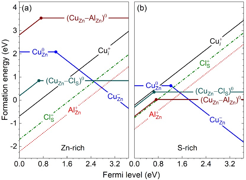
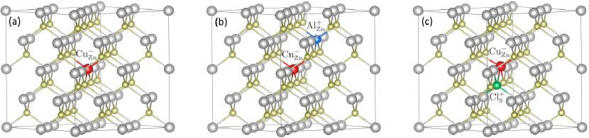
Next, we examine the effects of impurities, intentionally incorporated or otherwise. Figure 2 shows the calculated formation energies of ZnS doped with Cu, Al, or Cl, or co-doped with (Cu,Al) or (Cu,Cl). The substitutional Cu impurity, CuZn, is stable as Cu (i.e., Cu2+) under p-type conditions or Cu (i.e., Cu+) under n-type conditions and introduces a deep acceptor level at 1.22 eV above the VBM. This calculated value is in excellent agreement with the experimental one (1.25 eV) reported in the literature.Shionoya (2006) The result also indicates that CuZn does not contribute to p-type conductivity, at least at not too high doping levels. The atomic structure of Cu is presented in Fig. 3(a). The impurity is tetrahedrally coordinated with sulfur; the Cu–S bond length is 2.333 Å (), compared to 2.345 Å of the Zn–S bonds in bulk ZnS.
The Cu interstitial, Cui, is stable as Cu (i.e., Cu+) in the entire range of Fermi-level values. In Cu, the Cu+ ion forms chemical bonds with four S atoms with the bond length of 2.360–2.366 Å. The defect is thus a shallow donor and can, in principle, cause n-type conductivity in the material. Its concentration under n-type conditions is, however, expected to be negligible compared to that of Cu due to the large difference in the formation energies; see Fig. 2. This appears to be consistent with experimental reports showing that there are negligible or no Cu interstitials in Cu-doped ZnS nanocrystals.Corrado et al. (2009); Car et al. (2011)
Regarding AlZn and ClS, they are stable as Al and Cl, respectively, over the entire range of Fermi-level values. Like in the case of Cui, these defects donate one electron to the host and become ionized; the electron then transfers to the CBM. AlZn and ClS are thus shallow donors, which is consistent with experimental observations.Yamaga et al. (1988); Yasuda et al. (1997) In Al, the Al–S bond length is 2.272 Å (), whereas in Cl the local lattice environment is slightly more distorted with Cl–Zn bonds of 2.559 Å () and 2.563 Å. These impurities are often found in ZnS-based luminescent materials.Shionoya (2006); Corrado et al. (2009) Note that the n-type conductivityShionoya (2006) usually observed in as-grown single crystals of ZnS could be due to the presence of unintentional AlZn or ClS impurities. The observed conductivity may also be caused by the presence of other (intentional or otherwise) impurities not yet considered here. For example, it has been reported that hydrogen incorporated on the S site, HS, behaves as a shallow donor in wurtzite ZnS.Varley and Lordi (2013)
The above impurities, especially those with oppositely charged defect configurations, can form complexes. Explicit calculations are therefore carried out for CuZn–AlZn and CuZn–ClS. We find that these complexes are stable in the neutral charge state under n-type conditions or in the state under p-type conditions. The level is at 0.73 eV above the VBM for CuZn–AlZn and 0.66 eV for CuZn–ClS. The defect level is thus shifted, compared to that in the isolated CuZn, indicating strong local elastic and electrostatic interactions between the constituents in the complexes. In general, the electronic behavior of defect complexes can be significantly different from that of their isolated defects, a phenomenon also observed in other materials.Yan et al. (2012); Hoang (2016)
Figures 3(b) and 3(c) show the structure of (CuZn–AlZn)0 and (CuZn–ClS)0, respectively. In (CuZn–AlZn)0, the Cu–S bond lengths are 2.322 Å (), 2.324 Å, and 2.376 Å; the Al–S bond lengths are 2.281 Å(), 2.240 Å, and 2.284 Å. The binding energy is 0.57 eV with respect to the isolated (i.e., unassociated) constituents Cu and Al in the Fermi-level range eV (and hence under n-type conditions). In (CuZn–ClS)0, the Cu–S bond length is 2.258 Å () and the Cl–Zn bond length is 2.471 Å(); the Cu–Cl distance is 2.876 Å. The binding energy is 0.77 eV with respect to the isolated Cu and Cl in the Fermi-level range eV (and hence under n-type conditions). In both cases, the defect centers thus have lower symmetry than the host lattice. The binding energies are small, which suggests that the concentration of the complexes is likely much smaller than that of their isolated constituents when the material is prepared under thermodynamic equilibrium. The defect complexes are even less stable under p-type conditions: the binding energy of (CuZn–AlZn)+ is 0.08 eV with respect to isolated Cu and Al (in the range eV) and that of (CuZn–ClS)+ is 0.21 eV with respect to isolated Cu and Cl ( eV).
Given the calculated defect levels, the Cu-related defects can play a role in high-energy luminescent transitions in ZnS. An electron previously excited from the valence band to the conduction band or one at the shallow donor level such as that associated with Al or Cl in n-type ZnS, for example, can recombine with the empty defect state of the isolated Cu, resulting in a Cu Cu transition. The corresponding peak emission energy is eV, which is in the green region of the spectrum, with a relaxation energy of 0.16 eV; here, is given by the formation-energy difference between Cu and Cu, both in the lattice configuration of the initial configuration; see also Sec. II. For the CuZn–AlZn and CuZn–ClS complexes, the peak emission energies associated with the transition from the state to the neutral state is 2.79 eV and 2.81 eV with relaxation energies of 0.14 eV and 0.20 eV, respectively. Both the energies are thus in the blue region of the spectrum.
The isolated CuZn (i.e., CuZn that is not bound to a co-activator such as AlZn or ClS) is therefore a source of green luminescence in Cu-doped ZnS phosphors and CuZn–AlZn and CuZn–ClS complexes are sources of blue luminescence. As indicated above, the emission in all these cases is assumed to take place from the CBM to the (optical) transition level of the defect centers. The hydrogenic effective-mass state associated with a shallow donor such as AlZn or ClS is expected to be very close to the CBM. A schematic representation of these optical transitions and other energies, including the zero-phonon line (ZPL), is given in Fig. S2 in the Supplementary Material. Experimentally, it has been observed that the blue luminescent centers have lower symmetry than the host lattice whereas the symmetry is not lower in the case of the green luminescent center,Shionoya (2006); Corrado et al. (2009) which is consistent with our results and the analysis of the local lattice environment of CuZn vs. CuZn–AlZn and CuZn–ClS presented earlier.
The persistence of the luminescence observed in ZnS-based phosphorsShionoya (2006) could be due to electron trapping mediated by native defects. An electron excited from the valence band to the conduction band, for example, can be trapped in one of the defect levels , Zni, or ZnS introduce below the CBM (see Fig. 1). The electron can then be released back to the conduction band through some detrapping mechanism (e.g., thermal activation) and participate in the optical transitions discussed above. Whether , Zni, and/or ZnS are present in ZnS samples with significant concentrations likely depend on the synthesis conditions. Note that defects with a high formation energy may still form with high concentrations when the material is prepared under highly non-equilibrium conditions. In this case, a defect’s concentration is not directly determined by its formation energy.
Finally, in the (Cu,Al) and (Cu,Cl) doping, it is likely that both the isolated defects and defect complexes are present. As a result, the ZnS-based materials can exhibit both green and blue luminescence with different intensities. The concentration ratio between the unassociated CuZn and the CuZn–AlZn or CuZn–ClS complex is expected to depend on the Cu/Al or Cu/Cl ratio in the environment as well as other synthesis conditions. Experimentally, Chen et al., Chen et al. (2001) for example, found that the green (blue) emission is dominant at low (high) Cu concentrations. The observation can be understood as the following: At low Cu doping levels, the probability of Cu being close to the co-dopant (Al or Cl) is low; i.e., Cu is present in the material predominantly as the isolated CuZn. The probability of Cu being close to Al or Cl is, however, high at high Cu doping levels; as a result, Cu can be present predominantly in the defect complex form, CuZn–AlZn or CuZn–ClS. It is the defect–defect interaction within the defect complex that causes the shift from green to blue in the luminescence of these doped ZnS materials.
IV Conclusions
We have investigated native point defects and impurities in zincblende ZnS using hybrid density-functional calculations. Cation and anion vacancies and antisite defects are found to introduce deep defect levels in the band gap region and act as donors or acceptors depending on the position of the Fermi level. The Al and Cl impurities act as shallow donors whereas the Cu-related defects introduce deep defect levels. Significantly, we identify the unassociated CuZn is a source of green luminescence in ZnS-type phosphors and CuZn–AlZn and CuZn–ClS defect complexes are sources of blue luminescence.
Acknowledgements.
K.H. is grateful to Université de Nantes for supporting his visit to Institut des Matériaux Jean Rouxel (IMN) during which this work was initiated. This work used resources of the Extreme Science and Engineering Discovery Environment (XSEDE), which is supported by National Science Foundation Grant No. ACI-1548562, the National Energy Research Scientific Computing Center (NERSC), a U.S. Department of Energy Office of Science User Facility operated under Contract No. DE-AC02-05CH11231, the Center for Computationally Assisted Science and Technology (CCAST) at North Dakota State University, and Centre de Calcul Intensif des Pays de Loire (CCIPL), France.References
- Shionoya (2006) S. Shionoya, “Principal phosphor materials and their optical properties,” in Phosphor Handbook, CRC Press Laser and Optical Science and Technology Series, edited by S. Shionoya, W. M. Yen, and H. Yamamoto (CRC Press, 2006) pp. 247–274.
- Xu et al. (2018) X. Xu, S. Li, J. Chen, S. Cai, Z. Long, and X. Fang, “Design Principles and Material Engineering of ZnS for Optoelectronic Devices and Catalysis,” Adv. Funct. Mater. 28, 1802029 (2018).
- Li et al. (2012) P. Li, S. Deng, L. Zhang, G. Liu, and J. Yu, “Native point defects in ZnS: First-principles studies based on LDA, LDA+U and an extrapolation scheme,” Chem. Phys. Lett. 531, 75–79 (2012).
- Varley and Lordi (2013) J. B. Varley and V. Lordi, “Electrical properties of point defects in CdS and ZnS,” Appl. Phys. Lett. 103, 102103 (2013).
- Varley and Lordi (2014) J. B. Varley and V. Lordi, “Intermixing at the absorber-buffer layer interface in thin-film solar cells: The electronic effects of point defects in Cu(In,Ga)(Se,S)2 and Cu2ZnSn(Se,S)4 devices,” J. Appl. Phys. 116, 063505 (2014).
- Pham et al. (2015) H. H. Pham, G. T. Barkema, and L.-W. Wang, “DFT+U studies of Cu doping and p-type compensation in crystalline and amorphous ZnS,” Phys. Chem. Chem. Phys. 17, 26270–26276 (2015).
- Faghaninia et al. (2016) A. Faghaninia, K. R. Bhatt, and C. S. Lo, “Alloying ZnS in the hexagonal phase to create high-performing transparent conducting materials,” Phys. Chem. Chem. Phys. 18, 22628–22635 (2016).
- Ceperley and Alder (1980) D. M. Ceperley and B. J. Alder, “Ground State of the Electron Gas by a Stochastic Method,” Phys. Rev. Lett. 45, 566 (1980).
- Perdew et al. (1992) J. P. Perdew, J. A. Chevary, S. H. Vosko, K. A. Jackson, M. R. Pederson, D. J. Singh, and C. Fiolhais, “Atoms, molecules, solids, and surfaces: Applications of the generalized gradient approximation for exchange and correlation,” Phys. Rev. B 46, 6671–6687 (1992).
- Anisimov et al. (1991) V. I. Anisimov, J. Zaanen, and O. K. Andersen, “Hubbard-corrected density-functional theory,” Phys. Rev. B 44, 943–954 (1991).
- Perdew et al. (1996a) J. P. Perdew, M. Ernzerhof, and K. Burke, “Rationale for mixing exact exchange with density functional approximations,” J. Chem. Phys. 105, 9982–9985 (1996a).
- Bol et al. (2002) A. A. Bol, J. Ferwerda, J. A. Bergwerff, and A. Meijerink, “Luminescence of nanocrystalline ZnS:Cu2+,” J. Lumin. 99, 325–334 (2002).
- Corrado et al. (2009) C. Corrado, Y. Jiang, F. Oba, M. Kozina, F. Bridges, and J. Z. Zhang, “Synthesis, Structural, and Optical Properties of Stable ZnS:Cu,Cl Nanocrystals,” J. Phys. Chem. A 113, 3830–3839 (2009).
- Car et al. (2011) B. Car, S. Medling, C. Corrado, F. Bridges, and J. Z. Zhang, “Probing the local structure of dilute Cu dopants in fluorescent ZnS nanocrystals using EXAFS,” Nanoscale 3, 4182–4189 (2011).
- Heyd et al. (2003) J. Heyd, G. E. Scuseria, and M. Ernzerhof, “Hybrid functionals based on a screened Coulomb potential,” J. Chem. Phys. 118, 8207–8215 (2003).
- Kresse and Furthmüller (1996) G. Kresse and J. Furthmüller, “Efficient iterative schemes for ab initio total-energy calculations using a plane-wave basis set,” Phys. Rev. B 54, 11169–11186 (1996).
- Blöchl (1994) P. E. Blöchl, “Projector augmented-wave method,” Phys. Rev. B 50, 17953–17979 (1994).
- Freysoldt et al. (2014) C. Freysoldt, B. Grabowski, T. Hickel, J. Neugebauer, G. Kresse, A. Janotti, and C. G. Van de Walle, “First-principles calculations for point defects in solids,” Rev. Mod. Phys. 86, 253–305 (2014).
- Freysoldt et al. (2009) C. Freysoldt, J. Neugebauer, and C. G. Van de Walle, “Fully Ab Initio Finite-Size Corrections for Charged-Defect Supercell Calculations,” Phys. Rev. Lett. 102, 016402 (2009).
- Perdew et al. (1996b) J. P. Perdew, K. Burke, and M. Ernzerhof, “Generalized Gradient Approximation Made Simple,” Phys. Rev. Lett. 77, 3865–3868 (1996b).
- Yamaga et al. (1988) S. Yamaga, A. Yoshikawa, and H. Kasai, “Electrical and optical properties of donor doped ZnS films grown by low-pressure MOCVD,” J. Cryst. Growth 86, 252–256 (1988).
- Yasuda et al. (1997) T. Yasuda, B.-P. Zhang, and Y. Segawa, “MBE growth of n-type ZnSe and ZnS using ethylchloride as a dopant,” J. Cryst. Growth 175–176, 583–586 (1997).
- Yan et al. (2012) Q. Yan, A. Janotti, M. Scheffler, and C. G. Van de Walle, “Role of nitrogen vacancies in the luminescence of Mg-doped GaN,” Appl. Phys. Lett. 100, 142110 (2012).
- Hoang (2016) K. Hoang, “First-principles identification of defect levels in Er-doped GaN,” Phys. Status Solidi RRL 10, 915–918 (2016).
- Chen et al. (2001) Y. Y. Chen, J. G. Duh, B. S. Chiou, and C. G. Peng, “Luminescent mechanisms of ZnS:Cu:Cl and ZnS:Cu:Al phosphors,” Thin Solid Films 392, 50–55 (2001).