Strain-engineering of twist-angle in graphene/hBN superlattice devices
Abstract
The observation of novel physical phenomena such as Hofstadter’s butterfly, topological currents and unconventional superconductivity in graphene have been enabled by the replacement of SiO2 with hexagonal Boron Nitride (hBN) as a substrate and by the ability to form superlattices in graphene/hBN heterostructures. These devices are commonly made by etching the graphene into a Hall-bar shape with metal contacts. The deposition of metal electrodes, the design and specific configuration of contacts can have profound effects on the electronic properties of the devices possibly even affecting the alignment of graphene/hBN superlattices.
In this work we probe the strain configuration of graphene on hBN contacted with two types of metal contacts, two-dimensional (2D) top-contacts and one-dimensional (1D) edge-contacts. We show that top-contacts induce strain in the graphene layer along two opposing leads, leading to a complex strain pattern across the device channel. Edge-contacts, on the contrary, do not show such strain pattern. A finite-elements modelling simulation is used to confirm that the observed strain pattern is generated by the mechanical action of the metal contacts clamped to the graphene. Thermal annealing is shown to reduce the overall doping whilst increasing the overall strain, indicating and increased interaction between graphene and hBN. Surprisingly, we find that the two contacts configurations lead to different twist-angles in graphene/hBN superlattices, which converge to the same value after thermal annealing. This observation confirms the self-locking mechanism of graphene/hBN superlattices also in the presence of strain gradients. Our experiments may have profound implications in the development of future electronic devices based on heterostructures and provide a new mechanism to induce complex strain patterns in 2D materials.
keywords:
Graphene, hBN, superlattice, twist-angle, strain, RamanUniversity of Exeter]Centre for Graphene Science, College of Engineering, Mathematics and Physical Sciences, University of Exeter, Exeter EX4 4QF, United Kingdom \altaffiliationContributed equally to this work University of Exeter]Centre for Graphene Science, College of Engineering, Mathematics and Physical Sciences, University of Exeter, Exeter EX4 4QF, United Kingdom \altaffiliationContributed equally to this work University of Exeter]Centre for Graphene Science, College of Engineering, Mathematics and Physical Sciences, University of Exeter, Exeter EX4 4QF, United Kingdom \alsoaffiliation[University of Duhok]University of Duhok, Duhok, 42001 Kurdistan Region, Iraq University of Exeter]Centre for Graphene Science, College of Engineering, Mathematics and Physical Sciences, University of Exeter, Exeter EX4 4QF, United Kingdom University of Exeter]Centre for Graphene Science, College of Engineering, Mathematics and Physical Sciences, University of Exeter, Exeter EX4 4QF, United Kingdom University of Exeter]Centre for Graphene Science, College of Engineering, Mathematics and Physical Sciences, University of Exeter, Exeter EX4 4QF, United Kingdom
![[Uncaptioned image]](/html/1810.03903/assets/x1.png)
The high charge carrier mobility attained at room temperature in graphene encapsulated in hexagonal Boron Nitride (hBN)1 has enabled the observation of ballistic transport over macroscopic distances2, 3, 4 holding the promise for the development of room-temperature electrical equivalents of optical circuits. As opposed to suspended graphene structures5 in which low-energy flexural phonons impose severe limitations on the maximum value of charge carrier mobility observable at room temperature6, 7, in supported structures the optical phonons of the substrate play a central role. Compared to SiO2, the optical phonons in hBN have higher energy and this results in an increase of the charge carrier mobility in graphene by an order of magnitude1. Phonon scattering is not the only limiting factor to carrier mobility on SiO2, scattering from adsorbates such as water and substrate roughness also dominate its value. Being free from dangling bonds and lattice matched to graphene within , hBN also allows for an atomically clean interface to be formed. Crucially, the van der Waals attraction between these two-dimensional (2D) materials is strong enough to push contamination outside of the overlap region, resulting in an atomic-scale self cleaning mechanism which was shown to work for mechanically exfoliated flakes as well as large area graphene grown by chemical vapour deposition8, 3, 4. Another major breakthrough made possible by the encapsulation of graphene in hBN has been the realization of high-quality one-dimensional (1D) electrical contacts to graphene. In these edge-contact geometries, low temperature ballistic transport was reported over together with substrate-phonon limited room-temperature charge carrier mobility2.
Moiré interference patterns are observed for graphene on hBN owing to the small lattice mismatch between the two crystals. The rotation of graphene with respect to the underlying hBN produces patterns each with a different Moiré wavelength,9, 10 suggesting that effective periodic potentials are formed. For massless Dirac fermions this results in the formation of new Dirac points in the electronic band structure whose energy is determined by the Moiré wavelength.11 Superlattice structures have led to the observation of several physical phenomena including Hofstadter’s butterfly,12, 13, 14 topological currents,15 correlated insulator behaviour16 and unconventional superconductivity.17 Critical to these observations is the formation of a commensurate state in which graphene is locally stretched in domains separated by sharp domain walls. Previous works have reported a commensurate-incommensurate transition at twist-angles (i.e. the angle formed between the lattice vectors of graphene and hBN) of the order of the lattice mismatch ().18 For graphene forms these domains of strong van der Waals interaction with hBN, whilst in the opposing case () local strain is not observed. Thermal annealing has been shown to induce an incommensurate-commensurate transition over micrometer scales providing the initial twist-angle is small (). For flakes which do not align, a 1D network of wrinkles emerges due to the difference in thermal expansion coefficients between hBN and graphene.19
The quantum transport characteristics of twist-angle structures are commonly probed in transistor-like geometries. These generally consist of a graphene flake etched into a multi-terminal Hall-bar shape with metal contacts. However, the deposition of metal films onto graphene is known to induce structural defects, doping and strain20, 21, 22. Metal contacts are possibly responsible for the failure of the devices upon thermal annealing, cooling at cryogenic temperatures or further processing such as encapsulation in ionic gates23, 24. Ascertaining the role of the contacts on the properties of graphene/hBN superlattice structures is of pivotal importance and presently the focus of growing interest. For example, although phase- and growth-engineered 1D contacts have been explored in several atomically-thin materials25, 26, 27, the potential of 1D metallic edge-contacts for other encapsulated heterostructures has not yet been fully explored.
In this work we study the effect of strain induced by metal contacts in graphene/hBN superlattice devices. Semi-encapsulated graphene/hBN Hall-bars have been fabricated from a single flake with two different types of contact geometry: (1) two-dimensional (2D) top-contacts and (2) one-dimensional (1D) edge-contacts. Raman spectroscopy mapping was used to determine the strain and doping levels of the semi-encapsulated graphene. The absence of a top hBN layer allows to compare the two contact types in the same device. Top-contacts were found to induce strain levels up to , localised between two opposing leads, whilst edge-contacts do not induce any measurable strain. Surprisingly electrical transport measurements in devices encompassing the two types of contact geometry showed different twist-angles depending on the contact type, despite being fabricated on the same flake. Post-processing thermal annealing is shown to reduce the overall doping across the device, whilst increasing the overall strain. At the same time, the twist-angle is shown to change with thermal annealing resulting in its convergence to the same value for both contacts type. Our results are supported by finite elements method (FEM) simulations which correctly predict the observed strain pattern induced in graphene/hBN by top contacts geometries. Our studies unveil the interplay between strain and contact geometry in semi-encapsulated graphene on hBN. This knowledge could be instrumental in experimentally accessing the rich physics arising from the introduction of a gauge potential in the effective Hamiltonian of two-dimensional materials, such as the realisation of a purely strain-based valley filter28, 29 or a charge-funnelling device for energy applications30.
1 Strain in G/hBN Hall-bar devices
A single flake of monolayer graphene on hBN was used to fabricate Hall-bar devices (see methods) with two sets of metallic contacts, namely top- and edge-contacts, as schematically shown in figure 1a. The two sets of contacts have profound differences: edge electrodes make contact along a 1D chain of carbon atoms due to the etching step immediately before metal evaporation,2 whilst top electrodes overlap with the graphene flake, effectively making a 2D (or planar) electrical contact.31 A micrograph of the device is shown in figure 1b. No top hBN layer was used to encapsulate the device as this would forbid the fabrication of 2D top-contacts and, if used only for 1D edge-contacts, will not allow a direct comparison of the strain and doping levels in the underlying graphene.
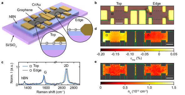
The Raman spectra acquired in the proximity of the two contacts (square and circle symbols in figure 1b) are shown in figure 1c. An immediate difference is visible: both the G and 2D modes of graphene ( and , respectively) are up-shifted for the edge- compared with top-contacts, whilst the phonon mode of hBN remains at in both cases.
Raman maps (see Methods) of the whole device are used to determine the strain and doping configuration of the graphene Hall-bar. The technique used is based on the work of Lee et al. 32 and illustrated in detail in Figures S2 and S3, Supporting Information, here we briefly outline it. The frequency of the G () and 2D () modes of graphene are extracted using a Lorentzian fit and plotted against each other. The data have a distribution which follows two principal axes crossing the pristine (unstrained and undoped) graphene coordinates (, )32. These axes represent the iso-doping and the iso-strain cases.32 From this plot it is possible to correlate and to the strain and (hole) doping levels by projecting each experimental point onto the principal axes and using the projected data to compute the strain and doping maps across the device.
Applying this method to the Hall-bar device in figure 1b we observe a clear distinction in the experimentally-determined level of strain () between the two contact regions, figure 1d. For the edge-contacts compressive strain is uniformly distributed across the graphene channel with an average value of , in agreement with literature.33 Conversely, for the top-contacts region, compressive strain is relaxed between opposing electrodes, with larger compressive strain levels in the central area between electrodes. In contrast to strain, the doping () is uniform across both top and edge contact geometries, figure 1e. A similar pattern is observed in a second device formed only by top-contacts, as shown in figure S4, Supporting Information.
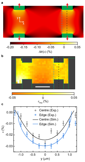
This experimental evidence suggests that top-contacts are “pulling” graphene, relaxing the existing compressive strain. To validate this idea, we perform a finite elements modelling (FEM) simulation and describe graphene as a two-dimensional, deformable membrane with an in-plane force applied normal to each contact region. Figure 2a shows the result of this analysis, where the difference between the simulated trace of the strain tensor and the initial compressive strain is plotted in a colour map (). Relaxation of the initial compressive strain is observed at the contacts and, more interestingly, a bow-tie feature is observed between opposing contacts. Both these features are present in the experimentally measured strain map, figure 2b. Figure 2c compares the experiment and simulated strain values for line-cuts in figure 2a,b with reasonable agreement between the two.
The relaxation of compressive strain in graphene by the metal electrodes can be understood in the following way. Metal deposition elevates the device temperature which subsequently cools once evaporation is complete. Given the difference between the thermal expansion coefficients of Au (positive) and graphene (negative), upon cooling graphene expands whilst gold contracts. This contraction dominates as the thermal expansion coefficient of gold () is greater than that of graphene ().34, 35 Therefore the contraction of the gold contacts relaxes the strained graphene with this relaxation extending into the channel area. While this is the case for top contacts, no strain relaxation is observed for edge contacts within the resolution of our experimental technique (), which can be explained by the order of magnitudes difference in the effective contact area between the two types of contacts. Edge-contacts in fully encapsulated devices are expected to induce similar strain level to the one observed in semi-encapsulated devices since the area of mechanical clamping to the graphene layer is the same.
2 Effect of annealing on strain patterns
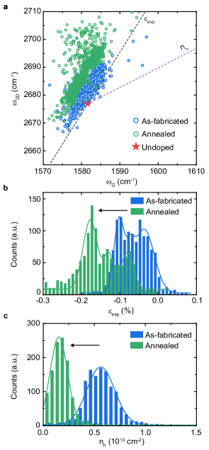
Thermal annealing is commonly used to enhance the electrical properties of graphene field-effect transistors by improving the metal-graphene interface and reducing contamination (e.g from polymer residues). However such procedure can lead to contact failure. In view of the observed strain pattern in our device, we study the effect of thermal annealing in this structure. Figure 3a shows the / distribution of the data from figure 1. In the as-fabricated device, the data are distributed along the iso-strain axis with a vertical shift away from the pristine case. This is thought to be due to Fermi velocity reduction, previously reported for graphene on hBN, which arises from van der Waals interlayer interaction.36, 37. Upon thermal annealing for hours in forming gas (H2/Ar, ) at the data-set shifts vertically upwards, suggesting a greater Fermi velocity reduction from increasing interlayer interaction (a strain/doping map of the device after thermal annealing is shown in figure S5, Supporting Information). Thermal treatment has a pronounced effect on the strain distribution, as shown in figure 3b. In the map shown in figure 1d it is possible to identify three distinct regions with different average strain levels, two coming from the top-contact region (strain emerging from opposing top contacts and the channel between adjacent pairs) and one from the edge-contact region (uniform strain). This suggests that the statistical distribution of the data (figure 3b) should be modelled with three Gaussian distributions. We confirm this observation by analysing the data extrapolated from each region, as detailed in figure S6, Supporting Information, where two distinct distributions are observed to arise from the top-contacts and one from the edge-contacts. Upon annealing, strain increases in all areas as evidenced by the values reported in table 1. Strain in the edge-contacted region increases from to () indicating that graphene has become more compressed. Similar compression is observed for top-contacts where close to (away from) the electrode an increase of () is extracted.
Previous reports have shown that graphene on hBN can undergo a rotation upon thermal annealing,19 increasing the crystallographic alignment, which occurs as the system tries to minimise the interlayer van der Waals energy. This suggests that there is a competition between flake rotation and mechanical clamping from the metal electrodes. With increased clamping from top contacts a smaller change in strain occurs in these regions. This observation highlights the potential negative role played by this phenomenon on the failure of contacts in graphene/hBN devices.
| (%) | ||||
|---|---|---|---|---|
| Contact Type | As-fabricated | Annealed | As-fabricated | Annealed |
| Edge | ||||
| Top (contact) | ||||
| Top (channel) | ||||
a Same value as previous.
Figure 3c shows a histogram of the doping levels used as an indication of contamination. In contrast to the strain statistics, a single Gaussian can be fitted to the data indicating uniform doping across both contact regions with . As expected, following annealing this reduces to , validating the usefulness of this common processing step in enhancing the electrical properties of graphene devices.
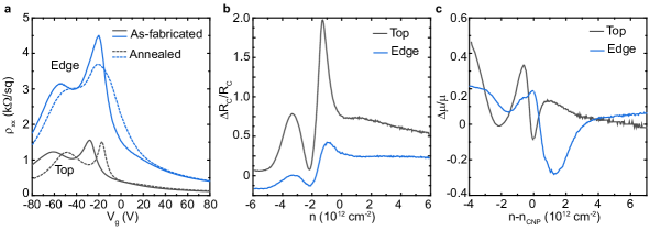
Electrical measurements help to shed light on the role of thermal annealing on strain for the different contact configurations. Figure 4a shows the resistivity () as a function of gate voltage () measured in the two contacts regions before and after thermal annealing. For both contact types, a down-shift of the charge neutrality point (CNP) after annealing is observed, with corresponding doping values comparable to those extrapolated from Raman spectroscopy. The change in contact resistance between the as-fabricated and annealed devices , where , and the corresponding change in mobility are shown in figure 4b and figure 4c, respectively. An increase by as much as of the contact resistance following annealing for top-contacts was observed, whereas a change of is observed for edge-contacts. This is in line with the observation that annealing top-contacts in the presence of strain can lead to their electrical failure. In top-contacts the presence of strain, due to the difference in thermal expansion between the metal and graphene, is an indication of good mechanical clamping. These contacts always result in good electrical connections. On the other hand, annealing of top-contacts with poor mechanical clamping which do not show measurable levels of strain in graphene result in open electrical contacts, see Supporting Information figure S7. This is in stark contrast to the observations reported on the edge-contacts which always result in good electrical connections in the absence of any measurable strain. Thermal annealing slightly improves the charge carrier mobility by the same amount () in both contact geometries, see figure 4c. This indicates that the charge carrier mobility is limited by Coulomb impurities and not by strain-induced modifications to the deformation potential acoustic phonon scattering.
3 Twist-angle in strained G/hBN superlattices
Two peaks in resistivity are observed in figure 4a. The CNP appears at () whilst a second, satellite peak, appears at . This second peak arises due to the emergence of additional Dirac points in the band structure of graphene on hBN, as previously observed in low-temperature transport experiments11, 38, 12, 13, 14 and more recently at room temperature39, 40 (see also figure S8, Supporting Information, for measurements on a second device).
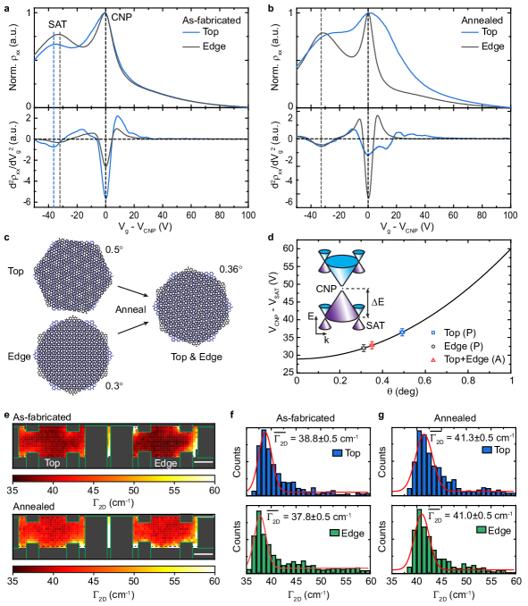
The interaction between hBN and graphene, which modifies the band structure of the latter, is tuned by the crystallographic angle between the two materials. This is reflected in a change of the separation of these two peaks in transport measurement which can be correlated to this angle.40 This separation is examined more closely in figure 5a,b. In the as-fabricated device the satellite peak () is at more negative gate voltages for edge regions. This can be clearly seen by taking the second derivative of the resistivity () indicating that different twist angles exist in the top and edge contact regions, a difference which disappears after annealing, figure 5b. Increasing the twist angle from reduces the Moiré wavelength () and manifests as a shift of the satellite Dirac points away from the main Dirac point (see figure 5d inset). The Moiré wavelength can be expressed as:11, 40
| (1) |
where is the lattice mismatch between graphene and hBN and is the lattice constant of graphene. Due to the spin and valley degeneracies in graphene, full-filling occurs at a density of four electrons per superlattice cell (), with the unit cell area .12 Since the carrier density is where is the geometric gate capacitance, is the position of the charge-neutrality point and is the electron charge, we find:
| (2) |
Using equation 1 and equation 2 it is therefore possible to extrapolate the twist-angle between graphene and hBN from the data in figure 5a,b. Figure 5c is a schematic illustration of the Moiré superlattice structure formed by rotating the graphene with respect to the hBN. Initially two twist angles are present, and . Upon thermal annealing, the heterostructure self-reorientates and one angle is measured for both regions (). In figure 5d the experimental data has been plotted with the functional dependence of against twist angle. Here, the free parameter is which has been estimated by considering the two dielectrics (hBN and SiO2) stacked in series.
The Moiré wavelength is related to the full-width at half-maximum (FWHM) of the 2D peak () by: , where the numerical constant () is dependent on the device structure and electrical properties (e.g. mobility)40. Given that this constant is unknown in our devices we cannot directly compare the absolute value of extrapolated from Raman and transport measurements. We are however able to confirm the convergence of the twist-angle after thermal annealing. Figure 5e shows the maps of obtained from the device in figure 1b before and after thermal annealing. The statistical distribution of for the two contact regions, before and after annealing, is shown in figure 5f,g. Before thermal annealing we obtain a difference in (centre of the Gaussian distribution) of . After annealing this value reduces to , confirming the convergence of the twist-angle observed in electronic transport measurements. Furthermore, the absolute values of after thermal annealing () are higher than the corresponding values before annealing (), suggesting that the twist-angles converge to a higher value, in apparent contrast with the data shown in figure 5d. Indeed, this is not the case as both the FWHM of the G peak () and the value of depend on strain33, with a slope . Therefore, the increase in after annealing confirms the data shown in figure 3a,b and supports the observation that thermal annealing increases the overall compressive strain.
4 Summary and discussion
To summarise, we have analysed the strain induced in single-layer graphene deposited on hBN by 2D top-contacts and 1D edge-contacts. Using Raman spectroscopy mapping, we have shown that top-contacts induce strain in the graphene flake, pulling in opposite directions. On the contrary, edge-contacts do not induce such strain. Our observation is supported by FEM simulations. We associate this strain to the shrinking of Au and graphene which, due to their different thermal expansion coefficients, lead to a net pull by the metal contacts after thermal evaporation of the metal. Thermal annealing on such devices reduces the overall doping, as expected from the removal of contaminants, but it also increases the overall compressive strain on the graphene. Such increase can lead to contacts failure given the observed strain pattern on the flake. Furthermore, on aligned samples, where the graphene and hBN lattice vectors are rotated by a small angle (), we have shown that the angle is different for the two types of contacts, although it converges to the same angle after thermal treatment. The convergence of the twist-angle confirms the self-locking mechanism observed in aligned graphene/hBN heterostructures19. The interplay between rotation and contacts-induced strain can also lead to contacts failure. Full encapsulation in hBN with edge-contacts may affect the way the angle changes upon annealing, however the negligible levels of strain observed in the edge-contacts suggest that this would not play a major role in this kind of devices.
Our observations elucidate the role of metal contacts on inducing strain in 2D materials-based electronic heterostructures. These findings can have profound implications on the development of future electronic applications based on layered two-dimensional materials in sensing and quantum computing. Metal contacts can be used to engineer complex strain patterns which could provide a system in which new physical phenomena could be investigated. The introduction of a gauge potential in the effective Hamiltonian, for example, can be used to realise a purely strain-based valley filter28, 29, whilst non-uniform bandgap modulation in semiconducting transition-metal dichalcogenides can be used in charge-funnelling devices for energy harvesting30.
Methods
Samples fabrication
Hexagonal Boron Nitride supplied by Manchester Nanomaterials was mechanically exfoliated onto SiO2/Si+ substrates that had been previously treated with a high power () O2 plasma. This processing step increases both the yield and lateral size of exfoliated flakes. Graphene was exfoliated onto a polymer bilayer (PMMA/PVA) and placed on the hBN by dry transfer.41 The lithography steps performed to create both top- and edge-contacts on the same flake are described in figure S1 and associated Supporting text. Electron beam lithography (Nano Beam NB5) was performed using -thick PMMA (MicroChem 950K A6), developed using a 3:1 solution of isopropanol (IPA) and 4-Methyl-2-pentanone (MIBK). Contacts were deposited using Cr/Au () thermal evaporation at pressure and lift off in hot Acetone (), then left overnight in Acetone. For edge-contacts, prior to metal deposition the exposed contact areas of the graphene/hBN stack were etched using a CHF3/O2 reactive-ion plasma at pressure with of CHF3 plus of O2, power for .
Electrical transport measurements
AC lock-in measurement techniques (Ametek Signal Recovery 7270) were employed to accurately probe changes in resistivity with small excitation voltages () minimising Joule heating in the device in a custom-built measurement chamber42. The excitation voltage was modulated at a frequency of . Two- () and four-terminal () voltages allowed the simultaneous measurement of channel resistivity, , field-effect mobility, , and contact resistance, . The graphene channel was capacitively coupled to the Si+ backgate through a -thick SiO2 layer, allowing the modulation of carrier density by applying a DC voltage. All measurements were performed in vacuum () at room temperature.
Raman spectroscopy
Raman spectra were acquired using a custom-built set-up with a excitation CW solid-state laser as source, focussed thorough a lens (NA, Olympus MPLFLN).43 Back-scattered light was collected by the same lens and, after filtration of the excitation line, dispersed by a grating mounted in a Princeton Instruments Acton SP2500 spectrometer and the spectra measured by a Princeton Instruments PIXIS400 CCD camera. The laser spot-size is , compatible with the lateral step-size of the motorised stage ()43. All measurements were performed in vacuum () at room temperature.
We have tested our system to perform the analysis outlined in the text in order to confirm the ability to resolve strain and doping levels, as detailed in figure S2. As shown in figure S3, for our test we employed a graphene flake deposited half on hBN and half on SiO2. Our analysis correctly showed a difference in both strain and doping in these two regions and highlighted an average compressive strain for graphene on hBN of , in agreement with literature.33
FEM simulations
FEM simulations were performed using Elmer open source multiphysical simulation software freely available from http://www.elmerfem.org. The built-in linear elasticity model solver was used. Graphene was simulated as a 2D membrane with a mesh containing nodes and surface elements. The physical size of the mesh was proportional to the actual device, shown in figure 1c, with a linear scaling factor of . The following elasticity parameters where used44: in-plane Young’s modulus and Poisson’s ratio . An in-plane force equivalent to was applied at opposing contacts in opposite directions. This is in good agreement with the stress-strain curve of graphene45.
Acknowledgment
We thank G. F. Jones for designing and building the vacuum chamber used in the Raman Spectroscopy measurements. M.F.C. and S.R. acknowledge financial support from: Engineering and Physical Sciences Research Council (EPSRC) of the United Kingdom, projects EP/M002438/1, EP/M001024/1, EPK017160/1, EP/K031538/1, EP/J000396/1; the Royal Society, grant title "Room temperature quantum technologies" and "Wearable graphene photovolotaic"; Newton fund, Uk-Brazil exchange grant title "Chronographene" and the Leverhulme Trust, research grants "Quantum drums" and "Quantum revolution". J.D.M. acknowledges financial support from the Engineering and Physical Sciences Research Council (EPSRC) of the United Kingdom, via the EPSRC Centre for Doctoral Training in Metamaterials, Grant No. EP/L015331/1. S.A. acknowledges financial support from the Higher Committee for Education Development in Iraq (HCED).
Author Contributions
A.D.S. and J.D.M. contributed equally to this work. A.D.S. and S.R. conceived the idea. A.D.S. performed the measurements, FEM simulations, interpreted the data and wrote the manuscript. J.D.M. fabricated the devices, interpreted the data and wrote the manuscript. S.A. fabricated the devices for initial studies and interpreted the data. F.W. developed the 2D material transfer system and demonstrated the transfer methods used for the production the graphene-hBN heterostructures. M.F.C. and S.R. supervised the project and wrote the paper.
Competing interests
The authors declare no competing financial interests.
Supporting Information is submitted in conjunction with this manuscript. Correspondence should be addressed to S.R. or A.D.S.
References
- Dean et al. 2010 Dean, C. R.; Young, A. F.; Meric, I.; Lee, C.; Wang, L.; Sorgenfrei, S.; Watanabe, K.; Taniguchi, T.; Kim, P.; Shepard, K. L.; Hone, J. Nature Nanotechnology 2010, 5, 722
- Wang et al. 2013 Wang, L.; Meric, I.; Huang, P. Y.; Gao, Q.; Gao, Y.; Tran, H.; Taniguchi, T.; Watanabe, K.; Campos, L. M.; Muller, D. A.; Guo, J.; Kim, P.; Hone, J.; Shepard, K. L.; Dean, C. R. Science 2013, 342, 614–617
- Banszerus et al. 2015 Banszerus, L.; Schmitz, M.; Engels, S.; Dauber, J.; Oellers, M.; Haupt, F.; Watanabe, K.; Taniguchi, T.; Beschoten, B.; Stampfer, C. Science Advances 2015, 1
- Banszerus et al. 2016 Banszerus, L.; Schmitz, M.; Engels, S.; Goldsche, M.; Watanabe, K.; Taniguchi, T.; Beschoten, B.; Stampfer, C. Nano Letters 2016, 16, 1387–1391
- Khodkov et al. 2015 Khodkov, T.; Khrapach, I.; Craciun, M. F.; Russo, S. Nano Letters 2015, 15, 4429–4433
- Mariani and von Oppen 2008 Mariani, E.; von Oppen, F. Phys. Rev. Lett. 2008, 100, 076801
- Castro et al. 2010 Castro, E. V.; Ochoa, H.; Katsnelson, M. I.; Gorbachev, R. V.; Elias, D. C.; Novoselov, K. S.; Geim, A. K.; Guinea, F. Phys. Rev. Lett. 2010, 105, 266601
- Kretinin et al. 2014 Kretinin, A. V.; Cao, Y.; Tu, J. S.; Yu, G. L.; Jalil, R.; Novoselov, K. S.; Haigh, S. J.; Gholinia, A.; Mishchenko, A.; Lozada, M.; Georgiou, T.; Woods, C. R.; Withers, F.; Blake, P.; Eda, G.; Wirsig, A.; Hucho, C.; Watanabe, K.; Taniguchi, T.; Geim, A. K.; Gorbachev, R. V. Nano Letters 2014, 14, 3270–3276
- Xue et al. 2011 Xue, J.; Sanchez-Yamagishi, J.; Bulmash, D.; Jacquod, P.; Deshpande, A.; Watanabe, K.; Taniguchi, T.; Jarillo-Herrero, P.; LeRoy, B. J. Nature Materials 2011, 10, 282
- Decker et al. 2011 Decker, R.; Wang, Y.; Brar, V. W.; Regan, W.; Tsai, H.-Z.; Wu, Q.; Gannett, W.; Zettl, A.; Crommie, M. F. Nano Letters 2011, 11, 2291–2295
- Yankowitz et al. 2012 Yankowitz, M.; Xue, J.; Cormode, D.; Sanchez-Yamagishi, J. D.; Watanabe, K.; Taniguchi, T.; Jarillo-Herrero, P.; Jacquod, P.; LeRoy, B. J. Nature Physics 2012, 8, 382
- Hunt et al. 2013 Hunt, B.; Sanchez-Yamagishi, J. D.; Young, A. F.; Yankowitz, M.; LeRoy, B. J.; Watanabe, K.; Taniguchi, T.; Moon, P.; Koshino, M.; Jarillo-Herrero, P.; Ashoori, R. C. Science 2013, 340, 1427–1430
- Dean et al. 2013 Dean, C. R.; Wang, L.; Maher, P.; Forsythe, C.; Ghahari, F.; Gao, Y.; Katoch, J.; Ishigami, M.; Moon, P.; Koshino, M.; Taniguchi, T.; Watanabe, K.; Shepard, K. L.; Hone, J.; Kim, P. Nature 2013, 497, 598
- Ponomarenko et al. 2013 Ponomarenko, L. A.; Gorbachev, R. V.; Yu, G. L.; Elias, D. C.; Jalil, R.; Patel, A. A.; Mishchenko, A.; Mayorov, A. S.; Woods, C. R.; Wallbank, J. R.; Mucha-Kruczynski, M.; Piot, B. A.; Potemski, M.; Grigorieva, I. V.; Novoselov, K. S.; Guinea, F.; Fal’ko, V. I.; Geim, A. K. Nature 2013, 497, 594
- Gorbachev et al. 2014 Gorbachev, R. V.; Song, J. C. W.; Yu, G. L.; Kretinin, A. V.; Withers, F.; Cao, Y.; Mishchenko, A.; Grigorieva, I. V.; Novoselov, K. S.; Levitov, L. S.; Geim, A. K. Science 2014, 346, 448–451
- Cao et al. 2018 Cao, Y.; Fatemi, V.; Demir, A.; Fang, S.; Tomarken, S. L.; Luo, J. Y.; Sanchez-Yamagishi, J. D.; Watanabe, K.; Taniguchi, T.; Kaxiras, E.; Ashoori, R. C.; Jarillo-Herrero, P. Nature 2018, 556, 80
- Cao et al. 2018 Cao, Y.; Fatemi, V.; Fang, S.; Watanabe, K.; Taniguchi, T.; Kaxiras, E.; Jarillo-Herrero, P. Nature 2018, 556, 43
- Woods et al. 2014 Woods, C. R.; Britnell, L.; Eckmann, A.; Ma, R. S.; Lu, J. C.; Guo, H. M.; Lin, X.; Yu, G. L.; Cao, Y.; Gorbachev, R. V.; Kretinin, A. V.; Park, J.; Ponomarenko, L. A.; Katsnelson, M. I.; Gornostyrev, Y. N.; Watanabe, K.; Taniguchi, T.; Casiraghi, C.; Gao, H.-J.; Geim, A. K.; Novoselov, K. S. Nature Physics 2014, 10, 451
- Woods et al. 2016 Woods, C. R.; Withers, F.; Zhu, M. J.; Cao, Y.; Yu, G.; Kozikov, A.; Ben Shalom, M.; Morozov, S. V.; van Wijk, M. M.; Fasolino, A.; Katsnelson, M. I.; Watanabe, K.; Taniguchi, T.; Geim, A. K.; Mishchenko, A.; Novoselov, K. S. Nature Communications 2016, 7, 10800
- Wang et al. 2011 Wang, W. X.; Liang, S. H.; Yu, T.; Li, D. H.; Li, Y. B.; Han, X. F. Journal of Applied Physics 2011, 109, 07C501
- Shioya et al. 2014 Shioya, H.; Craciun, M. F.; Russo, S.; Yamamoto, M.; Tarucha, S. Nano Letters 2014, 14, 1158–1163
- Shioya et al. 2015 Shioya, H.; Russo, S.; Yamamoto, M.; Craciun, M. F.; Tarucha, S. Nano Letters 2015, 15, 7943–7948
- Ye et al. 2011 Ye, J.; Craciun, M. F.; Koshino, M.; Russo, S.; Inoue, S.; Yuan, H.; Shimotani, H.; Morpurgo, A. F.; Iwasa, Y. Proceedings of the National Academy of Sciences 2011, 108, 13002–13006
- Mehew et al. 2017 Mehew, J. D.; Unal, S.; Torres Alonso, E.; Jones, G. F.; Fadhil Ramadhan, S.; Craciun, M. F.; Russo, S. Advanced Materials 2017, 29, 1700222
- Kappera et al. 2014 Kappera, R.; Voiry, D.; Yalcin, S. E.; Branch, B.; Gupta, G.; Mohite, A. D.; Chhowalla, M. Nature Materials 2014, 13, 1128
- Cho et al. 2015 Cho, S.; Kim, S.; Kim, J. H.; Zhao, J.; Seok, J.; Keum, D. H.; Baik, J.; Choe, D.-H.; Chang, K. J.; Suenaga, K.; Kim, S. W.; Lee, Y. H.; Yang, H. Science 2015, 349, 625–628
- Guimarães et al. 2016 Guimarães, M. H. D.; Gao, H.; Han, Y.; Kang, K.; Xie, S.; Kim, C.-J.; Muller, D. A.; Ralph, D. C.; Park, J. ACS Nano 2016, 10, 6392–6399
- Fujita et al. 2010 Fujita, T.; Jalil, M. B. A.; Tan, S. G. Applied Physics Letters 2010, 97, 043508
- Grujić et al. 2014 Grujić, M. M.; Tadić, M. i. c. v.; Peeters, F. m. c. M. Phys. Rev. Lett. 2014, 113, 046601
- De Sanctis et al. 2018 De Sanctis, A.; Amit, I.; Hepplestone, S. P.; Craciun, M. F.; Russo, S. Nature Communications 2018, 9, 1652
- Allain et al. 2015 Allain, A.; Kang, J.; Banerjee, K.; Kis, A. Nature Materials 2015, 14, 1195
- Lee et al. 2012 Lee, J. E.; Ahn, G.; Shim, J.; Lee, Y. S.; Ryu, S. Nature Communications 2012, 3, 1024
- Neumann et al. 2015 Neumann, C.; Reichardt, S.; Venezuela, P.; Drögeler, M.; Banszerus, L.; Schmitz, M.; Watanabe, K.; Taniguchi, T.; Mauri, F.; Beschoten, B.; Rotkin, S. V.; Stampfer, C. Nature Communications 2015, 6, 8429
- Bao et al. 2009 Bao, W.; Miao, F.; Chen, Z.; Zhang, H.; Jang, W.; Dames, C.; Lau, C. N. Nature Nanotechnology 2009, 4, 562
- Yoon et al. 2011 Yoon, D.; Son, Y.-W.; Cheong, H. Nano Letters 2011, 11, 3227–3231
- Hwang et al. 2012 Hwang, C.; Siegel, D. A.; Mo, S.-K.; Regan, W.; Ismach, A.; Zhang, Y.; Zettl, A.; Lanzara, A. Scientific Reports 2012, 2, 590
- Ahn et al. 2013 Ahn, G.; Kim, H. R.; Ko, T. Y.; Choi, K.; Watanabe, K.; Taniguchi, T.; Hong, B. H.; Ryu, S. ACS Nano 2013, 7, 1533–1541
- Yang et al. 2013 Yang, W.; Chen, G.; Shi, Z.; Liu, C.-C.; Zhang, L.; Xie, G.; Cheng, M.; Wang, D.; Yang, R.; Shi, D.; Watanabe, K.; Taniguchi, T.; Yao, Y.; Zhang, Y.; Zhang, G. Nature Materials 2013, 12, 792
- Tang et al. 2015 Tang, S.; Wang, H.; Wang, H. S.; Sun, Q.; Zhang, X.; Cong, C.; Xie, H.; Liu, X.; Zhou, X.; Huang, F.; Chen, X.; Yu, T.; Ding, F.; Xie, X.; Jiang, M. Nature Communications 2015, 6, 6499
- Ribeiro-Palau et al. 2018 Ribeiro-Palau, R.; Zhang, C.; Watanabe, K.; Taniguchi, T.; Hone, J.; Dean, C. R. Science 2018, 361, 690–693
- Pizzocchero et al. 2016 Pizzocchero, F.; Gammelgaard, L.; Jessen, B. S.; Caridad, J. M.; Wang, L.; Hone, J.; Bøggild, P.; Booth, T. J. Nature Communications 2016, 7, 11894
- De Sanctis et al. 2018 De Sanctis, A.; Mehew, J. D.; Alkhalifa, S.; Tate, C. P.; White, A.; Woodgate, A. R.; Craciun, M. F.; Russo, S. Review of Scientific Instruments 2018, 89, 024705
- De Sanctis et al. 2017 De Sanctis, A.; Jones, G. F.; Townsend, N. J.; Craciun, M. F.; Russo, S. Review of Scientific Instruments 2017, 88, 055102
- Politano and Chiarello 2015 Politano, A.; Chiarello, G. Nano Research 2015, 8, 1847–1856
- Fthenakis and Lathiotakis 2015 Fthenakis, Z. G.; Lathiotakis, N. N. Phys. Chem. Chem. Phys. 2015, 17, 16418–16427